
 My Inquiry
 My Account


NXP Semiconductors MC68HC000FN16R2
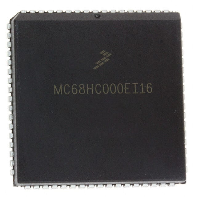
- Part No.:
- MC68HC000FN16R2
- Manufacturer:
- NXP Semiconductors
- Category:
- Microprocessors
- Package:
- 68-LCC (J-Lead)
- Datasheet:
-
 MC68HC000FN16R2.pdf
- Description:
- IC MPU M680X0 16MHZ 68PLCC
- Quantity:
- Payment:

- Shipping:

Inventory:4,970
Please send an inquiry. Send us your inquiry, and we will respond immediately.
Product details
Overview
MC68HC000FN16R2 from Freescale Semiconductor (formerly Motorola) is a CMOS 16-bit microprocessor compatible with the M68000 architecture, featuring a 16-bit external data bus, 24-bit address bus supporting up to 16 MB memory space, and 16 MHz maximum clock frequency. It operates from a single +5 V supply and implements full supervisor/user privilege modes for embedded control applications including industrial PLCs and legacy instrumentation systems.
For engineers reviewing the MC68HC000FN16R2 datasheet, MC68HC000FN16R2 pinout, MC68HC000FN16R2 application, or MC68HC000FN16R2 equivalent, key selection criteria include bus timing compatibility with 8/16-bit peripherals, asynchronous bus control support (DTACK, BERR), interrupt vectoring capability, and thermal performance in through-hole industrial environments.
Technical Context
The MC68HC000FN16R2 executes the full M68000 instruction set with identical programmer's model-16 general-purpose registers (8 data, 7 address, 1 stack pointer), 16-bit ALU, and status register with interrupt mask and privilege bits. Its bus interface supports both synchronous and fully asynchronous operation via DTACK handshake, enabling direct connection to slow memory and peripherals without wait-state generators.
It features three-level interrupt priority handling (autovector, spurious, and user-defined vectors), bus arbitration support (BR/BG), and exception processing with dedicated stack frames for bus error, address error, and reset. Unlike the original HMOS MC68000, this HC variant uses CMOS technology for lower power consumption and improved noise immunity at 16 MHz.
Key Specifications
| Parameter | Value and Actual Design Meaning |
|---|---|
| Max Clock Frequency | 16 MHz - defines maximum instruction throughput and real-time response latency in deterministic control loops. |
| Data Bus Width | 16-bit external - enables efficient transfer of word-aligned data; requires external byte-lane steering for 8-bit peripheral interfacing. |
| Address Bus Width | 24-bit - supports 16 MB linear address space, sufficient for ROM/RAM-mapped I/O in mid-complexity embedded systems. |
| Supply Voltage | +5 V ±5% - compatible with standard TTL/CMOS logic families and legacy power supplies in industrial backplanes. |
| Process Technology | CMOS - reduces active power dissipation to ~1.2 W typical at 16 MHz, enabling convection-cooled operation in sealed enclosures. |
| Interrupt Inputs | Three level-sensitive lines (IPL0–IPL2) - provides hardware-prioritized vectored interrupt handling without external priority encoder. |
| Bus Control Signals | DTACK, BERR, HALT, BR/BG - enables robust asynchronous bus timing, error recovery, and multi-master arbitration in shared-bus systems. |
Pinout & Package
MC68HC000FN16R2 is housed in a 68-lead Quad Flat Pack (QFP) package per Case 778-02 (FN suffix), with 0.65 mm lead pitch and exposed thermal pad. The package supports through-hole or surface-mount assembly depending on board design requirements.
| Pin/Terminal | Circuit Role | Design Meaning |
|---|---|---|
| CLK | Clock Input | Accepts TTL-compatible square wave; internal two-phase clock generation enables synchronous internal timing without external phase splitter. |
| AS | Address Strobe | Indicates valid address on AB; used by memory/peripheral to latch address before data transfer begins. |
| DS | Data Strobe | Active-low signal indicating valid data on DB during read/write cycles; synchronized with DTACK for timing margin. |
| DTACK | Data Transfer Acknowledge | Handshake signal allowing variable-length bus cycles; permits direct interface to slow devices without fixed wait states. |
| BERR | Bus Error | Asynchronous error indication causing exception vector fetch; used for memory-mapped I/O fault detection and recovery. |
| IPL0–IPL2 | Interrupt Priority Level | Three-level encoded input determining interrupt vector offset; supports nested interrupt servicing without software polling. |
| RESET | Reset Input | Active-low asynchronous reset initializing PC, SR, and all registers to known state; asserts after power stabilization. |
| VCC / GND | Power Supply | +5 V supply and ground pins distributed across package corners and center for low-impedance decoupling and EMI reduction. |
Key Features
| Feature | Design Value |
|---|---|
| Full M68000 Instruction Set Compatibility | Executes identical binary code as MC68000, enabling drop-in replacement in existing designs with no firmware changes required. |
| CMOS Process Implementation | Reduces typical power consumption by >60% vs. HMOS MC68000 at same frequency, lowering thermal management complexity. |
| Asynchronous Bus Interface | Eliminates need for fixed wait-state generators; DTACK-driven timing adapts to diverse memory/peripheral access speeds. |
| Dual Privilege Mode Operation | Enables secure separation of kernel and application code via supervisor/user mode switching and status register protection. |
| Hardware Interrupt Vectoring | Automatically loads vector address from memory on interrupt, reducing latency and eliminating software polling overhead. |
Applications
| Industrial PLC Controller | Legacy Test Equipment |
|---|---|
Use Scenario: Standalone programmable logic controller executing ladder logic scans in 10–100 ms cycles with discrete I/O expansion. IC Role / Device Role / Timing Role: Central execution unit managing scan timing, I/O mapping, and serial HMI communication via UART peripheral. Use Value: Deterministic 16 MHz instruction execution ensures consistent scan intervals; 24-bit addressing supports modular I/O memory maps up to 16 MB. |
Use Scenario: Automated calibration system for analog multimeters requiring precise timing, EEPROM-based configuration storage, and GPIB interface. IC Role / Device Role / Timing Role: Main controller coordinating ADC sampling, EEPROM writes, and GPIB command parsing with strict timing deadlines. Use Value: Asynchronous DTACK interface allows reliable handshake with slow EEPROM write cycles; BERR detection prevents corrupted calibration data writes. |
| Avionics Maintenance Terminal | Medical Imaging Subsystem |
Use Scenario: Ruggedized field terminal for aircraft subsystem diagnostics, running real-time OS with CAN and ARINC-429 interfaces. IC Role / Device Role / Timing Role: Host processor managing dual-channel serial protocol stacks and non-volatile fault log storage. Use Value: Three-level IPL inputs enable prioritized handling of time-critical ARINC-429 receive interrupts over background CAN polling. |
Use Scenario: Embedded subsystem in ultrasound machine controlling beamforming FPGA configuration and sensor data buffering. IC Role / Device Role / Timing Role: Configuration manager loading FPGA bitstreams from flash and validating checksums before activation. Use Value: Bus error exception handling detects invalid flash reads, triggering safe fallback to factory configuration without system reset. |
Equivalent & Alternatives
The following parts are listed as comparable options for similar microprocessor applications.
| Alternative Part | Technical Difference | Application Difference | Selection Advice |
|---|---|---|---|
| MC68EC000RC16 | 3.3 V core voltage, no VMA output, reduced peripheral support; lacks BERR and HALT signals. | Suitable only for new low-power designs with modern 3.3 V peripherals; not pin-compatible or software-compatible without voltage translation and firmware adaptation. | Select only when migrating to 3.3 V infrastructure and redesigning bus interface logic. |
| MC68000P12 | HMOS process, 12 MHz max, +5 V only, higher power (2.5 W typical), no CMOS noise immunity. | Compatible with legacy 12 MHz systems but requires additional heat sinking and suffers greater susceptibility to EMI in noisy industrial settings. | Prefer only for exact form-fit-function replacement where MC68HC000FN16R2 availability is constrained and thermal headroom exists. |
Compared with MC68HC000FN16R2, the MC68EC000RC16 offers lower voltage operation but sacrifices bus robustness and legacy compatibility, while the MC68000P12 retains full functional equivalence at lower speed and higher power-making the MC68HC000FN16R2 the optimal balance of performance, power, and backward compatibility for industrial retrofits.
Availability
MC68HC000FN16R2 is available at Aetrix Electronics and suitable for industrial PLC controllers, legacy test equipment, avionics maintenance terminals, and medical imaging subsystems requiring stable component supply and long-term obsolescence management.
Supply support for MC68HC000FN16R2 includes scheduled delivery planning, volume procurement assistance, BOM continuity management, traceable sourcing, and lifecycle availability coordination for OEM customers, industrial embedded developers, connected-device designers, and electronics production programs.
Manufacturer
Freescale Semiconductor (now part of NXP Semiconductors) was a leading designer of embedded processors, known for its M68K family and automotive microcontrollers.
The MC68HC000 belongs to Freescale's legacy M68000 microprocessor line, designed for high-reliability industrial, instrumentation, and aerospace applications requiring binary compatibility with earlier HMOS variants and robust asynchronous bus operation.
FAQ
What is the maximum operating frequency of the MC68HC000FN16R2?
The MC68HC000FN16R2 is rated for a maximum clock frequency of 16 MHz under specified voltage and temperature conditions. This rating is validated per Freescale's AC Electrical Specifications-Clock Timing section, and corresponds to guaranteed instruction execution timing across all addressing modes and bus cycles. Operating the MC68HC000FN16R2 above 16 MHz may result in undefined behavior or timing violations.
Does the MC68HC000FN16R2 support 8-bit peripheral interfacing?
Yes, the MC68HC000FN16R2 supports 8-bit peripheral interfacing through its 16-bit data bus using byte-select control (UDS/LDS signals). External logic can gate upper or lower data lanes during transfers, and the processor automatically adjusts cycle timing based on DTACK assertion. This capability is documented in Section 4 (8-Bit Bus Operations) of the M68000 User's Manual.
Is the MC68HC000FN16R2 pin-compatible with the original MC68000P12?
No, the MC68HC000FN16R2 is not pin-compatible with the MC68000P12. While both share the same 68-pin footprint in DIP packages, the MC68HC000FN16R2 uses a 68-lead QFP (Case 778-02), whereas the MC68000P12 uses a 64-pin DIP. Signal assignments also differ-for example, VMA is absent on the HC variant, and power/ground pin distribution is reorganized for thermal performance.
What interrupt handling capabilities does the MC68HC000FN16R2 provide?
The MC68HC000FN16R2 provides three level-sensitive interrupt inputs (IPL0–IPL2) supporting seven priority levels, autovectoring for six predefined exceptions, and user-defined vector addresses for custom handlers. It implements full exception stack frame preservation per Section 6 of the M68000 User's Manual, including supervisor/user mode switching and status register masking-enabling deterministic real-time interrupt response in safety-critical applications.
How does the MC68HC000FN16R2 manage bus errors during memory access?
The MC68HC000FN16R2 uses the BERR (Bus Error) signal to asynchronously trigger a bus error exception, which forces a vector fetch from address $000004 and pushes a complete stack frame containing program counter, status register, and fault address. This mechanism-detailed in Section 6.3.9-is essential for detecting invalid memory accesses, failed peripheral handshakes, or misconfigured address decoding in deployed systems.
MC68HC000FN16R2 Specifications
- Product attributes
- Attribute value
- Manufacturer:
- NXP Semiconductors
- Package/Case:
- 68-LCC (J-Lead)
- Series:
- M680x0
- Packaging:
- Tape & Reel (TR)
- Product Status:
- Obsolete
- Core Processor:
- EC000
- Number of Cores/Bus Width:
- 1 Core, 32-Bit
- Speed:
- 16MHz
- Co-Processors/DSP:
- -
- RAM Controllers:
- -
- Graphics Acceleration:
- No
- Display & Interface Controllers:
- -
- Ethernet:
- -
- SATA:
- -
- USB:
- -
- Voltage - I/O:
- 5.0V
- Operating Temperature:
- 0°C ~ 70°C (TA)
- Grade:
- -
- Qualification:
- -
- Security Features:
- -
- Mounting Type:
- Surface Mount
- Supplier Device Package:
- 68-PLCC (24.21x24.21)
- Additional Interfaces:
- -
MC68HC000FN16R2 FAQ
1.How can I place an order for MC68HC000FN16R2 through Aetrix?
Please submit a Request for Quotation (RFQ) for MC68HC000FN16R2 on Aetrix. Our sales agent will provide a competitive quotation and guide you through the order confirmation once you accept the terms.
2.Are the price and stock information for MC68HC000FN16R2 reliable?
The price and inventory of MC68HC000FN16R2 are updated periodically and may fluctuate due to market conditions. Stock and pricing data are typically refreshed every 24 hours. Quotation validity for MC68HC000FN16R2 is usually 5 days.
3.What payment methods are accepted for MC68HC000FN16R2?
We accept Wire Transfer, PayPal, Credit Card, Western Union, MoneyGram, and Escrow for MC68HC000FN16R2 transactions.
Note: Certain payment methods may incur a processing fee.
4.How is shipping managed for MC68HC000FN16R2?
MC68HC000FN16R2 orders can be shipped via leading logistics carriers, including DHL, UPS, FedEx, TNT, or Registered Mail.
Once your MC68HC000FN16R2 order is processed, you will receive an email with the shipment details and tracking number.
Note: Tracking information may take up to 24 hours to appear. Express delivery typically takes 3–5 business days.
5.How can I obtain technical support or documentation for MC68HC000FN16R2?
For technical support, including MC68HC000FN16R2 datasheets, pinout diagrams, or application guidance, please contact our engineering support team. They can provide detailed documentation and assistance for your MC68HC000FN16R2 requirements.
6.How does Aetrix verify that MC68HC000FN16R2 is sourced from the original manufacturer or authorized distributors?
All MC68HC000FN16R2 products on Aetrix are procured from qualified distributors and authorized channels. Our dedicated quality assurance team conducts strict verification, including traceability checks and, if necessary, third-party testing. This ensures that MC68HC000FN16R2 meets industry standards.
7.What is the process for return or replacement of MC68HC000FN16R2?
All MC68HC000FN16R2 units undergo pre-shipment inspection (PSI). If there is an issue with MC68HC000FN16R2, returns or replacements are accepted under the following conditions:
1.Quantity discrepancies, incorrect items, or visible external defects (such as breakage or corrosion), acknowledged by Aetrix.
2.The issue is reported within 90 days of delivery.
3.The MC68HC000FN16R2 part is unused and in its original packaging.
Return procedure for MC68HC000FN16R2:
1.Submit a request within 90 days.
2.Obtain a Return Material Authorization (RMA) from Aetrix.
MC68HC000FN16R2 Tags

-
AT91SAM9260B-CU-999
Microchip Technology
-
AT91SAM9G25-CU
Microchip Technology

-
ATSAMA5D27C-CU
Microchip Technology
-
AT91SAM9X35-CU
Microchip Technology
-
AT91SAM9X25-CU
Microchip Technology

-
MCIMX6Y2CVM08AB
NXP Semiconductors
.JPG)
-
AM3352BZCZ100
Texas Instruments
-
AT91SAM9260B-CU
Microchip Technology

-
AT91SAM9260B-QU
Microchip Technology

-
ATSAMA5D31A-CU
Microchip Technology
-
AT91SAM9G20B-CU-999
Microchip Technology
-
MCIMX6Y2CVM05AB
NXP Semiconductors
Tech Hub

A practical engineering guide to 3.3V and 5V logic compatibility, input thresholds, resistor dividers, translator ICs, MOSFET level shifting, I2C pull-ups, timing limits and power-sequencing risks.

The 74HC595 uses push-pull logic outputs, while the TPIC6B595 uses 50 V open-drain DMOS sinks for higher-power loads. This guide compares timing, current limits, 3.3 V interfacing, load wiring, thermal…

The 74HC595 converts serial data into eight stable parallel outputs. This guide covers pin functions, shift and storage timing, OE and MR behavior, drive-current limits, cascading, voltage compatibilit…

A technical comparison of level-sensitive latches and edge-triggered flip-flops, covering timing windows, setup and hold limits, master–slave operation, time borrowing, race-through, HDL inference and…

A D latch stores one bit while Enable controls when data can pass. This reference covers gate-level operation, truth tables, transparency, setup and hold timing, LE versus OE, common ICs and practical …

An SR latch stores one bit through cross-coupled feedback. This engineering reference covers NOR and NAND implementations, truth tables, forbidden-state recovery, gated operation, switch debouncing, fa…

Latch circuits retain one bit through feedback. This technical reference covers SR and D latches, truth tables, transparency, timing limits, latch-versus-flip-flop behavior, applications and common log…

An engineering guide to LED driver operation, constant-current and constant-voltage outputs, linear and switching topologies, dimming, IC selection, calculations, replacement compatibility, and fault c…

Operational amplifier guide covering op amp basics, feedback, ideal vs real op amps, common configurations, buffer circuits, offset, bias current, gain-bandwidth, slew rate, rail-to-rail limits and sel…

Jumper cables guide covering safe connection order, red and black clamp placement, final ground connection, cable gauge, length, clamp quality, copper vs CCA cables, jump starter comparison and battery…


