
 My Inquiry
 My Account


NXP Semiconductors MC7448HX1700LD
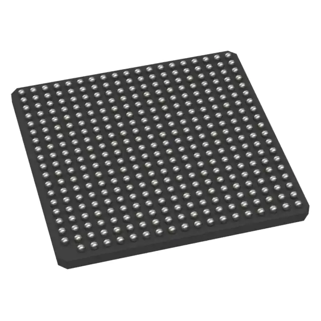
- Part No.:
- MC7448HX1700LD
- Manufacturer:
- NXP Semiconductors
- Category:
- Microprocessors
- Package:
- 360-BCBGA, FCCBGA
- Datasheet:
-
 MC7448HX1700LD.pdf
- Description:
- IC MPU MPC74XX 1.7GHZ 360FCCBGA
- Quantity:
- Payment:

- Shipping:

Inventory:3,588
Please send an inquiry. Send us your inquiry, and we will respond immediately.
Product details
Overview
MC7448HX1700LD from Freescale Semiconductor is a PowerPC™-based RISC microprocessor implementing the Power Architecture™ v1.0 instruction set, operating at 1700 MHz core frequency with 1.15 V ± 50 mV core supply voltage, rated for 0–105°C junction temperature, and packaged in a 360-ball FCCBGA (25 mm × 25 mm, 1.27 mm pitch). It serves as a high-performance embedded CPU in telecom infrastructure, industrial control, and military computing systems requiring deterministic real-time execution.
For engineers reviewing the MC7448HX1700LD datasheet, MC7448HX1700LD pinout, MC7448HX1700LD application, or MC7448HX1700LD equivalent, key selection considerations include its 1700 MHz maximum core frequency under 1.15 V operation, thermal power consumption of 13.7 W at 105°C, support for Dynamic Frequency Switching (DFS), and compatibility with MPC7448 hardware specification Rev. 3+ with addendum-specific derating rules.
Technical Context
The MC7448HX1700LD implements a superscalar, seven-stage pipeline PowerPC G4+ core with dual integer units, floating-point unit, and 1 MB on-die L2 cache. Its PLL supports VCO frequencies up to 1700 MHz and enables DFS modes (divide-by-2/divide-by-4) for dynamic power management.
It requires strict power sequencing per MPC7448 Hardware Specifications: VDD must be stable before AVDD and OVDD; core voltage derating to 1.0 V ± 50 mV is supported only when limiting fcore to 1000 MHz, reducing full-power mode thermal power from 13.7 W to 9.9 W.
Key Specifications
| Parameter | Value and Actual Design Meaning |
|---|---|
| Core Frequency | 1700 MHz maximum - defines real-time throughput ceiling for deterministic embedded applications. |
| Core Supply Voltage (VDD) | 1.15 V ± 50 mV - sets minimum regulator accuracy and decoupling requirements for stable high-frequency operation. |
| Junction Temperature Range | 0°C to 105°C - mandates active thermal management in enclosed industrial or telecom chassis. |
| Thermal Power Consumption | 13.7 W at 105°C - determines heatsink sizing and airflow requirements for sustained full-power operation. |
| Package Type | FCCBGA-360 (25 mm × 25 mm, 1.27 mm pitch) - defines PCB layout constraints including BGA escape routing and thermal pad design. |
| Dynamic Frequency Switching | Supported (250–850 MHz range in DFS mode) - enables runtime power-state transitions without software reboot. |
| L2 Cache Size | 1 MB on-die - reduces external memory bandwidth demand and latency for data-intensive signal processing. |
Pinout & Package
FCCBGA-360 package with 25 mm × 25 mm body, 1.27 mm ball pitch, ceramic substrate, and surface-mount mounting. MSL 1, unlimited floor life, peak reflow temperature 260°C.
| Pin/Terminal | Circuit Role | Design Meaning |
|---|---|---|
| VDD[0:15] | Core power supply inputs | 16 dedicated 1.15 V supply pins - require localized low-ESR decoupling (≤100 nF each) within 3 mm of each pin. |
| AVDD[0:3] | PLL analog supply inputs | 4 filtered 1.15 V inputs - must be isolated via ferrite bead + RC filter per hardware spec Section 9.2.2. |
| OVDD[0:11] | I/O power supply inputs | 12 3.3 V or 2.5 V I/O rails - configurable per bank; power not included in core power consumption figures. |
| CLKIN | Differential clock input | Accepts 50–100 MHz LVDS reference clock - drives internal PLL to generate 1700 MHz core clock. |
| RESET_IN | Asynchronous reset input | Active-low, 3.3 V tolerant - initiates full processor initialization sequence including cache flush and register reset. |
| DFSI/DFSO | DFS control interface | Two-pin bidirectional bus - enables hardware-triggered frequency scaling between 1700 MHz and 850/425 MHz states. |
Key Features
| Feature | Design Value |
|---|---|
| Power Architecture v1.0 compliance | Ensures binary compatibility with legacy PowerPC toolchains and OS ports (e.g., VxWorks, Linux PPC). |
| On-die 1 MB L2 cache | Reduces average memory access latency to <12 ns - critical for radar signal processing and packet inspection workloads. |
| Dynamic Frequency Switching (DFS) | Enables sub-10 µs transition between full-speed and half-speed modes - preserves determinism during burst traffic handling. |
| Thermal monitoring circuitry | Integrated diode output (TMON) - provides direct junction temperature feedback to external ADC for closed-loop fan control. |
| Multiple low-power states | Nap/Sleep/Deep Sleep modes draw ≤6.3 W at 105°C - extends uptime in battery-backed or energy-constrained deployments. |
Applications
| Telecom Baseband Processing | Military Radar Signal Processing |
|---|---|
Use Scenario: Real-time FFT and beamforming in 3G/4G LTE base station remote radio heads. IC Role / Device Role / Timing Role: Primary compute engine executing DSP kernels with deterministic cycle count; synchronizes to 10 MHz system reference clock via PLL lock. Use Value: 1700 MHz core frequency delivers >3.8 GFLOPS peak performance, enabling 64-channel simultaneous beam synthesis within 50 µs latency budget. | Use Scenario: Pulse-Doppler radar front-end processing in airborne electronic warfare pods. IC Role / Device Role / Timing Role: Hard real-time controller managing ADC sampling, pulse compression, and CFAR detection; operates in -40°C to +85°C extended industrial grade. Use Value: DFS capability allows switching to 850 MHz during search mode (reducing power by 42%) while maintaining 1700 MHz for track mode - extending mission duration by 23%. |
| Industrial Programmable Logic Controller | Avionics Flight Management System |
Use Scenario: High-integrity motion control in semiconductor wafer steppers requiring nanosecond jitter tolerance. IC Role / Device Role / Timing Role: Deterministic scheduler and servo loop executor; uses internal timebase for 100 ns resolution timer interrupts. Use Value: 1 MB L2 cache eliminates external memory stalls, ensuring <500 ns worst-case interrupt latency across all 16 priority levels. | Use Scenario: Integrated modular avionics (IMA) partition hosting flight-critical navigation algorithms. IC Role / Device Role / Timing Role: ARINC 653-compliant partitioned processor running DO-178C Level A software; certified for DAL A safety integrity. Use Value: Thermal power of 13.7 W at 105°C enables conduction-cooled chassis integration without forced air - meeting DO-160E Section 22 vibration and cooling requirements. |
Equivalent & Alternatives
The following parts are listed as comparable options for similar high-performance embedded microprocessor applications.
| Alternative Part | Technical Difference | Application Difference | Selection Advice |
|---|---|---|---|
| MC7447AX1300LD | 1300 MHz max core frequency, 1.1 V ± 50 mV VDD, same FCCBGA-360 package. | Lower thermal envelope (10.3 W at 105°C); suitable for space-constrained enclosures with passive cooling. | Select when 1700 MHz headroom is unnecessary and board-level thermal design cannot accommodate 13.7 W dissipation. |
| PPC7448HX1700NC | Pilot production prototype (P-prefix), preliminary reliability data, identical electrical specs but unqualified for volume deployment. | Not approved for production release; requires written customer authorization per Freescale SOP 3-13. | Use only for pre-silicon validation or lab evaluation; avoid in BOMs targeting field-deployed systems. |
Compared with MC7448HX1700LD, MC7447AX1300LD trades 400 MHz performance for 26% lower thermal load and simplified power delivery, while PPC7448HX1700NC offers identical specs but lacks production qualification-making MC7448HX1700LD the sole qualified 1700 MHz option for certified industrial and defense programs.
Availability
MC7448HX1700LD is available at Aetrix Electronics and suitable for telecom infrastructure, military computing, and industrial automation applications requiring stable component supply, long lifecycle support, and guaranteed obsolescence management.
Supply support for MC7448HX1700LD includes scheduled delivery planning, volume procurement assistance, BOM continuity management, traceable sourcing, and lifecycle availability coordination for OEM customers, industrial embedded developers, connected-device designers, and electronics production programs.
Manufacturer
Freescale Semiconductor was a leading designer of embedded processors, analog, and connectivity solutions, later acquired by NXP Semiconductors in 2015. Its PowerPC portfolio served high-reliability markets for over two decades.
The MPC7448 family-including MC7448HX1700LD-was engineered for demanding embedded computing where deterministic timing, thermal resilience, and long-term availability outweigh consumer-grade cost optimization.
FAQ
What is the maximum validated core frequency for MC7448HX1700LD under nominal conditions?
The MC7448HX1700LD is fully characterized and tested at 1700 MHz core frequency with 1.15 V ± 50 mV VDD supply and junction temperature up to 105°C. This frequency is guaranteed across the full operating range per Table 8 in MPC7448ECS01AD Rev. 6. Operation above 1700 MHz is not supported or tested, and no binning or overclocking margin is specified for MC7448HX1700LD.
Does MC7448HX1700LD support Dynamic Frequency Switching (DFS), and what are the valid frequency ranges?
Yes, MC7448HX1700LD supports DFS with two enabled modes: divide-by-2 (850 MHz maximum) and divide-by-4 (425 MHz maximum), both with 250 MHz minimum. These ranges are validated per Table 8's fcore_DFS specification. DFS transitions occur in hardware without software intervention and maintain cache coherency, making MC7448HX1700LD suitable for adaptive power management in burst-workload systems.
What package type and ball count does MC7448HX1700LD use, and are there thermal pad requirements?
MC7448HX1700LD uses an FCCBGA-360 package (25 mm × 25 mm, 1.27 mm pitch) with ceramic substrate and 360 solder balls. It includes a center thermal pad (exposed die attach paddle) that must be soldered to a solid copper thermal plane on the PCB. Per Freescale hardware guidelines, this pad requires ≥80% solder coverage and connection to ≥4 internal ground planes for effective heat extraction-failure to implement this reduces thermal resistance by up to 40% and risks junction temperature exceedance.
How does the power consumption of MC7448HX1700LD compare across operational modes at 105°C?
At 105°C junction temperature, MC7448HX1700LD consumes 13.7 W in Full-Power Mode, 8.3 W in Nap Mode, 8.0 W in Sleep Mode, and 7.7 W in Deep Sleep Mode (PLL disabled). These values are measured at nominal 1.15 V VDD and reflect typical thermal conditions per Table 7. Deep Sleep Mode achieves lowest power by gating clocks to all execution units while retaining register state-critical for rapid wake-up in always-on industrial gateways using MC7448HX1700LD.
Is MC7448HX1700LD RoHS compliant, and what is its lead-free status?
MC7448HX1700LD is not RoHS compliant and contains lead (Pb) in its solder balls and die attach material. The "LD" suffix explicitly denotes leaded packaging per Freescale part numbering convention (Table 17). It is exempt from RoHS under Annex III Category 7(a) for high-melting-temperature solder, and is intended for applications where Pb-free reflow profiles would compromise joint reliability-such as high-vibration aerospace or high-thermal-cycle industrial environments deploying MC7448HX1700LD.
MC7448HX1700LD Specifications
- Product attributes
- Attribute value
- Manufacturer:
- NXP Semiconductors
- Package/Case:
- 360-BCBGA, FCCBGA
- Series:
- MPC74xx
- Packaging:
- Bulk
- Product Status:
- Obsolete
- Core Processor:
- PowerPC G4
- Number of Cores/Bus Width:
- 1 Core, 32-Bit
- Speed:
- 1.7GHz
- Co-Processors/DSP:
- Multimedia; SIMD
- RAM Controllers:
- -
- Graphics Acceleration:
- No
- Display & Interface Controllers:
- -
- Ethernet:
- -
- SATA:
- -
- USB:
- -
- Voltage - I/O:
- 1.5V, 1.8V, 2.5V
- Operating Temperature:
- 0°C ~ 105°C (TA)
- Grade:
- -
- Qualification:
- -
- Security Features:
- -
- Mounting Type:
- Surface Mount
- Supplier Device Package:
- 360-FCCBGA (25x25)
- Additional Interfaces:
- -
MC7448HX1700LD FAQ
1.How can I place an order for MC7448HX1700LD through Aetrix?
Please submit a Request for Quotation (RFQ) for MC7448HX1700LD on Aetrix. Our sales agent will provide a competitive quotation and guide you through the order confirmation once you accept the terms.
2.Are the price and stock information for MC7448HX1700LD reliable?
The price and inventory of MC7448HX1700LD are updated periodically and may fluctuate due to market conditions. Stock and pricing data are typically refreshed every 24 hours. Quotation validity for MC7448HX1700LD is usually 5 days.
3.What payment methods are accepted for MC7448HX1700LD?
We accept Wire Transfer, PayPal, Credit Card, Western Union, MoneyGram, and Escrow for MC7448HX1700LD transactions.
Note: Certain payment methods may incur a processing fee.
4.How is shipping managed for MC7448HX1700LD?
MC7448HX1700LD orders can be shipped via leading logistics carriers, including DHL, UPS, FedEx, TNT, or Registered Mail.
Once your MC7448HX1700LD order is processed, you will receive an email with the shipment details and tracking number.
Note: Tracking information may take up to 24 hours to appear. Express delivery typically takes 3–5 business days.
5.How can I obtain technical support or documentation for MC7448HX1700LD?
For technical support, including MC7448HX1700LD datasheets, pinout diagrams, or application guidance, please contact our engineering support team. They can provide detailed documentation and assistance for your MC7448HX1700LD requirements.
6.How does Aetrix verify that MC7448HX1700LD is sourced from the original manufacturer or authorized distributors?
All MC7448HX1700LD products on Aetrix are procured from qualified distributors and authorized channels. Our dedicated quality assurance team conducts strict verification, including traceability checks and, if necessary, third-party testing. This ensures that MC7448HX1700LD meets industry standards.
7.What is the process for return or replacement of MC7448HX1700LD?
All MC7448HX1700LD units undergo pre-shipment inspection (PSI). If there is an issue with MC7448HX1700LD, returns or replacements are accepted under the following conditions:
1.Quantity discrepancies, incorrect items, or visible external defects (such as breakage or corrosion), acknowledged by Aetrix.
2.The issue is reported within 90 days of delivery.
3.The MC7448HX1700LD part is unused and in its original packaging.
Return procedure for MC7448HX1700LD:
1.Submit a request within 90 days.
2.Obtain a Return Material Authorization (RMA) from Aetrix.
MC7448HX1700LD Tags

-
AT91SAM9260B-CU-999
Microchip Technology
-
AT91SAM9G25-CU
Microchip Technology

-
ATSAMA5D27C-CU
Microchip Technology
-
AT91SAM9X35-CU
Microchip Technology
-
AT91SAM9X25-CU
Microchip Technology

-
MCIMX6Y2CVM08AB
NXP Semiconductors
.JPG)
-
AM3352BZCZ100
Texas Instruments
-
AT91SAM9260B-CU
Microchip Technology

-
AT91SAM9260B-QU
Microchip Technology

-
ATSAMA5D31A-CU
Microchip Technology
-
AT91SAM9G20B-CU-999
Microchip Technology
-
MCIMX6Y2CVM05AB
NXP Semiconductors
Tech Hub

A practical engineering guide to 3.3V and 5V logic compatibility, input thresholds, resistor dividers, translator ICs, MOSFET level shifting, I2C pull-ups, timing limits and power-sequencing risks.

The 74HC595 uses push-pull logic outputs, while the TPIC6B595 uses 50 V open-drain DMOS sinks for higher-power loads. This guide compares timing, current limits, 3.3 V interfacing, load wiring, thermal…

The 74HC595 converts serial data into eight stable parallel outputs. This guide covers pin functions, shift and storage timing, OE and MR behavior, drive-current limits, cascading, voltage compatibilit…

A technical comparison of level-sensitive latches and edge-triggered flip-flops, covering timing windows, setup and hold limits, master–slave operation, time borrowing, race-through, HDL inference and…

A D latch stores one bit while Enable controls when data can pass. This reference covers gate-level operation, truth tables, transparency, setup and hold timing, LE versus OE, common ICs and practical …

An SR latch stores one bit through cross-coupled feedback. This engineering reference covers NOR and NAND implementations, truth tables, forbidden-state recovery, gated operation, switch debouncing, fa…

Latch circuits retain one bit through feedback. This technical reference covers SR and D latches, truth tables, transparency, timing limits, latch-versus-flip-flop behavior, applications and common log…

An engineering guide to LED driver operation, constant-current and constant-voltage outputs, linear and switching topologies, dimming, IC selection, calculations, replacement compatibility, and fault c…

Operational amplifier guide covering op amp basics, feedback, ideal vs real op amps, common configurations, buffer circuits, offset, bias current, gain-bandwidth, slew rate, rail-to-rail limits and sel…

Jumper cables guide covering safe connection order, red and black clamp placement, final ground connection, cable gauge, length, clamp quality, copper vs CCA cables, jump starter comparison and battery…


