
 My Inquiry
 My Account


NXP Semiconductors MC9328MXLVP20
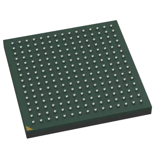
- Part No.:
- MC9328MXLVP20
- Manufacturer:
- NXP Semiconductors
- Category:
- Microprocessors
- Package:
- 225-LFBGA
- Datasheet:
-
 MC9328MXLVP20.pdf
- Description:
- IC MPU I.MXL 200MHZ 225MAPBGA
- Quantity:
- Payment:

- Shipping:

Inventory:3,889
Please send an inquiry. Send us your inquiry, and we will respond immediately.
Product details
Overview
MC9328MXLVP20 from NXP Semiconductors (formerly Freescale) is an ARM920T™-based applications processor operating at 200 MHz, featuring integrated SDRAM controller, LCD controller, USB Device, MMC/SD host controller, and multimedia accelerator. It targets portable multimedia devices requiring low-power, high-integration SoC solutions with 225-ball MAPBGA packaging.
For engineers reviewing the MC9328MXLVP20 datasheet, MC9328MXLVP20 pinout, MC9328MXLVP20 application, or MC9328MXLVP20 equivalent, key selection criteria include core frequency (200 MHz), I/O voltage range (1.7–3.3 V), operating temperature (0°C to 70°C), 225-ball MAPBGA package compatibility, and integrated peripheral support for LCD, USB, and SD interfaces.
Technical Context
The MC9328MXLVP20 implements an ARM920T™ core with Harvard architecture, 16 KB instruction and 16 KB data caches, and a Memory Management Unit (MMU). Its system-level integration includes an External Interface Module (EIM) supporting NOR/NAND flash and SRAM, dual UARTs with IrDA/Auto-bauding, and a DMA controller with 11 channels.
Power management is handled by a DPLL clock and power control module enabling dynamic voltage/frequency scaling. The processor supports both big- and little-endian operation via the BIG_ENDIAN pin and provides dedicated video port signals (CSI_D[7:0], CSI_VSYNC, CSI_HSYNC) for CMOS sensor interfacing alongside LCD timing outputs (FLM/VSYNC, LP/HSYNC, LSCLK).
Key Specifications
| Parameter | Value and Actual Design Meaning |
|---|---|
| Core Architecture | ARM920T™ 32-bit RISC CPU with MMU, 16 KB I-cache + 16 KB D-cache |
| Maximum Core Frequency | 200 MHz - enables real-time multimedia processing in portable devices |
| I/O Supply Voltage Range | 1.7 V to 3.3 V - supports mixed-voltage peripheral interfacing including 3.3 V SD/USB/LCD |
| Core Supply Voltage Range | 1.8 V to 2.0 V at 200 MHz - requires precise low-noise regulation for stable high-frequency operation |
| Operating Temperature | 0°C to 70°C - qualified for commercial portable electronics environments |
| Package Type | 225-contact MAPBGA (Case 1304B-01) - 1.0 mm ball pitch, 13 mm × 13 mm footprint |
| Integrated Peripherals | SDRAMC, LCDC, USB Device, MMC/SD Host, CSI, SPI ×2, UART ×2, I²C, SSI/I²S, PWM, RTC, Watchdog - reduces external component count for handheld designs |
Pinout & Package
MC9328MXLVP20 is housed in a 225-ball Molded Array Process Ball Grid Array (MAPBGA), Case 1304B-01, with 1.0 mm ball pitch and 13 mm × 13 mm body size. Power and ground balls are distributed across multiple VDD/VSS pairs (NVDD1–NVDD4, QVDD1–QVDD4, AVDD1, NVSS, QVSS) to support independent supply domains for digital I/O, core logic, and analog functions.
| Pin/Terminal | Circuit Role | Design Meaning |
|---|---|---|
| A0–A24 | Address Bus (EIM) | 25-bit multiplexed address for external memory and peripherals; A[24:0] used in non-SDRAM cycles |
| D[31:0] | Data Bus (EIM) | 32-bit bidirectional data path supporting burst transfers and byte-enable control (EB0–EB3) |
| SDCLK, SDRAMC signals | SDRAM Timing Interface | Includes SDCLK, RAS, CAS, SDWE, CSD0/CSD1, DQM[3:0], MA[11:0], SDBA[4:0] - fully compliant with JEDEC SDRAM standards |
| LD[15:0], FLM/VSYNC, LP/HSYNC | LCD Controller Outputs | 16-bit parallel RGB/YUV data bus + frame/line sync signals for direct TFT panel driving |
| USBD_VP/VM, USBD_SUSPND | USB 1.1 Device Interface | Differential DP/DM pins with suspend signaling - requires external 1.5 kΩ pull-up on USBD_VP for full-speed enumeration |
| CSI_D[7:0], CSI_PIXCLK | CMOS Sensor Interface | 8-bit parallel video data path with pixel clock, VSYNC, HSYNC - supports raw Bayer or YUV sensor output |
Key Features
| Feature | Design Value |
|---|---|
| ARM920T™ Core with MMU | Enables Linux and other protected-memory OS execution with virtual memory management |
| Integrated Multimedia Accelerator (MMA) | Offloads JPEG encode/decode and MPEG-4 SP decoding from CPU, reducing active power in media playback |
| Dual UARTs with Auto-Bauding & IrDA | Supports legacy serial diagnostics and infrared communication without external level shifters or baud-rate configuration |
| Memory Stick® Host Controller (MSHC) | Direct interface to Sony Memory Stick cards - eliminates need for external card-interface bridge ICs |
| Flexible Power Domains (QVDD/NVDD/AVDD) | Allows independent voltage scaling per functional block - e.g., 2.0 V core / 3.3 V SDIO / 1.8 V analog sensors |
Applications
| Handheld Media Player | Industrial HMI Terminal |
|---|---|
Use Scenario: Portable device playing MP3, WMA, and MPEG-4 video with touch-enabled UI and SD card storage. IC Role / Device Role / Timing Role: Primary applications processor executing OS, managing LCD display, decoding audio/video streams, and controlling SD/MMC storage. Use Value: Integrated LCDC, USB Device, and MMC/SD host eliminate discrete interface ICs; MMA accelerates decode latency below 100 ms for smooth 30 fps video. | Use Scenario: Factory-floor operator interface with resistive touchscreen, local data logging, and RS-485 connectivity. IC Role / Device Role / Timing Role: Central controller running real-time embedded Linux, driving monochrome or color TFT display, and managing serial communications via UART2. Use Value: Dual UARTs with hardware flow control (RTS/CTS) and built-in watchdog ensure deterministic response; 0°C to 70°C rating matches industrial ambient requirements. |
| Smartphone Baseband Companion | Digital Photo Frame |
Use Scenario: Secondary processor in early 2000s smartphones handling UI rendering, camera preview, and multimedia while main baseband handles RF. IC Role / Device Role / Timing Role: Offloads graphics, camera sensor capture (via CSI), and LCD refresh from baseband SoC using shared memory over EIM. Use Value: CSI interface synchronizes to sensor pixel clock; LCDC supports programmable timing for diverse panel types; 225-ball MAPBGA fits compact PCB layouts. | Use Scenario: Wall-mounted photo display loading JPEG images from SD card and showing transitions on TFT screen. IC Role / Device Role / Timing Role: Standalone image processor reading files from SD, decoding JPEG via MMA, and driving 320×240 or 480×272 LCD at 60 Hz. Use Value: Integrated SD host and LCDC reduce BOM to microSD socket + LCD + power regulator; low 1.8 V core voltage extends battery life in always-on mode. |
Equivalent & Alternatives
The following parts are listed as comparable options for similar applications processor applications.
| Alternative Part | Technical Difference | Application Difference | Selection Advice |
|---|---|---|---|
| MC9328MXLVP15 | 150 MHz ARM920T™ core; identical 225-ball MAPBGA package and peripheral set | Lower performance ceiling; suitable for cost-sensitive or thermally constrained designs where 200 MHz is unnecessary | Select when system throughput requirements are ≤150 MHz and thermal budget limits full-speed operation |
| i.MX21ADS | Reference design board (not IC); based on MC9328MXL but includes full evaluation hardware, debug interface, and preloaded firmware | Not a drop-in replacement - serves as development platform rather than production component | Use for prototyping and software validation before committing to MC9328MXLVP20 in final BOM |
Compared with MC9328MXLVP15, the MC9328MXLVP20 delivers 33% higher CPU throughput for multimedia tasks; compared with i.MX21ADS, it is the bare die IC requiring full custom carrier board design but offers full production scalability and cost optimization.
Availability
MC9328MXLVP20 is available at Aetrix Electronics and suitable for handheld media players, industrial HMIs, and digital photo frames requiring stable component supply, long-term lifecycle support, and verified legacy SoC sourcing.
Supply support for MC9328MXLVP20 includes scheduled delivery planning, volume procurement assistance, BOM continuity management, traceable sourcing, and lifecycle availability coordination for OEM customers, industrial embedded developers, connected-device designers, and electronics production programs.
Manufacturer
NXP Semiconductors (acquired Freescale in 2015) is a global semiconductor leader focused on secure connectivity solutions for automotive, industrial, IoT, and mobile applications.
The i.MX family - including MC9328MXLVP20 - was designed specifically for portable multimedia appliances, emphasizing power efficiency, peripheral integration, and ARM-based software compatibility in resource-constrained handheld devices.
FAQ
What is the maximum operating frequency of the MC9328MXLVP20?
The MC9328MXLVP20 operates at a guaranteed maximum core frequency of 200 MHz under specified conditions: QVDD = 1.8–2.0 V, TA = 0°C to 70°C. This frequency is validated across process, voltage, and temperature corners per Freescale's Rev. 8 datasheet. The MC9328MXLVP20 does not support overclocking beyond this rated speed, and sustained operation above 200 MHz may result in timing violations or data corruption.
Does the MC9328MXLVP20 support DDR SDRAM?
No, the MC9328MXLVP20 supports only single-data-rate (SDR) SDRAM, as confirmed by its SDRAM controller documentation, signal naming (SDCLK, RAS, CAS, SDWE), and timing diagrams in the Rev. 8 datasheet. It lacks DDR-specific signals such as DQS, DM, or ODT control. The MC9328MXLVP20 SDRAMC complies with JEDEC Standard No. 22, which defines SDR SDRAM - not DDR or LPDDR. For DDR support, later i.MX generations (e.g., i.MX31) must be considered.
What package type and ball count does the MC9328MXLVP20 use?
The MC9328MXLVP20 uses a 225-contact Mold Array Process Ball Grid Array (MAPBGA), designated Case 1304B-01, with 1.0 mm ball pitch and 13 mm × 13 mm body size. This matches the "VP" suffix in the part number (vs. "VM" for 256-ball variant). Pin assignments and power ball distribution are documented in Table 3 of the MC9328MXL Technical Data Rev. 8, confirming 225 unique solder balls including NVDD, QVDD, AVDD, and NVSS/QVSS domains.
Can the MC9328MXLVP20 operate with a 1.7 V core supply?
No - the MC9328MXLVP20 requires a minimum core supply (QVDD) of 1.8 V when operating at 200 MHz, as specified in Table 5 (Recommended Operating Range) of the Rev. 8 datasheet. At 1.7 V, the device is only rated for ≤150 MHz operation (as in MC9328MXLVP15). Attempting 200 MHz operation at 1.7 V violates electrical specifications and risks setup/hold time failures, cache coherency errors, or unpredictable resets.
Is the MC9328MXLVP20 pin-compatible with the MC9328MXLVM20?
No - the MC9328MXLVP20 (225-ball MAPBGA) and MC9328MXLVM20 (256-ball MAPBGA) have different packages, ball counts, and pinouts. They share identical functionality and register maps, but mechanical and electrical pin mapping differs significantly: e.g., SDCLK appears on R8 in VP20 but on T10 in VM20; LD15 is on F13 in VP20 but on P15 in VM20. PCB layout is not interchangeable, and no adapter or footprint conversion is supported.
MC9328MXLVP20 Specifications
- Product attributes
- Attribute value
- Manufacturer:
- NXP Semiconductors
- Package/Case:
- 225-LFBGA
- Series:
- i.MXL
- Packaging:
- Tray
- Product Status:
- Obsolete
- Core Processor:
- ARM920T
- Number of Cores/Bus Width:
- 1 Core, 32-Bit
- Speed:
- 200MHz
- Co-Processors/DSP:
- -
- RAM Controllers:
- SDRAM
- Graphics Acceleration:
- No
- Display & Interface Controllers:
- LCD
- Ethernet:
- -
- SATA:
- -
- USB:
- USB 1.x (1)
- Voltage - I/O:
- 1.8V, 3.0V
- Operating Temperature:
- 0°C ~ 70°C (TA)
- Grade:
- -
- Qualification:
- -
- Security Features:
- -
- Mounting Type:
- Surface Mount
- Supplier Device Package:
- 225-MAPBGA (13x13)
- Additional Interfaces:
- I2C, I2S, SPI, SSI, MMC/SD, UART
MC9328MXLVP20 FAQ
1.How can I place an order for MC9328MXLVP20 through Aetrix?
Please submit a Request for Quotation (RFQ) for MC9328MXLVP20 on Aetrix. Our sales agent will provide a competitive quotation and guide you through the order confirmation once you accept the terms.
2.Are the price and stock information for MC9328MXLVP20 reliable?
The price and inventory of MC9328MXLVP20 are updated periodically and may fluctuate due to market conditions. Stock and pricing data are typically refreshed every 24 hours. Quotation validity for MC9328MXLVP20 is usually 5 days.
3.What payment methods are accepted for MC9328MXLVP20?
We accept Wire Transfer, PayPal, Credit Card, Western Union, MoneyGram, and Escrow for MC9328MXLVP20 transactions.
Note: Certain payment methods may incur a processing fee.
4.How is shipping managed for MC9328MXLVP20?
MC9328MXLVP20 orders can be shipped via leading logistics carriers, including DHL, UPS, FedEx, TNT, or Registered Mail.
Once your MC9328MXLVP20 order is processed, you will receive an email with the shipment details and tracking number.
Note: Tracking information may take up to 24 hours to appear. Express delivery typically takes 3–5 business days.
5.How can I obtain technical support or documentation for MC9328MXLVP20?
For technical support, including MC9328MXLVP20 datasheets, pinout diagrams, or application guidance, please contact our engineering support team. They can provide detailed documentation and assistance for your MC9328MXLVP20 requirements.
6.How does Aetrix verify that MC9328MXLVP20 is sourced from the original manufacturer or authorized distributors?
All MC9328MXLVP20 products on Aetrix are procured from qualified distributors and authorized channels. Our dedicated quality assurance team conducts strict verification, including traceability checks and, if necessary, third-party testing. This ensures that MC9328MXLVP20 meets industry standards.
7.What is the process for return or replacement of MC9328MXLVP20?
All MC9328MXLVP20 units undergo pre-shipment inspection (PSI). If there is an issue with MC9328MXLVP20, returns or replacements are accepted under the following conditions:
1.Quantity discrepancies, incorrect items, or visible external defects (such as breakage or corrosion), acknowledged by Aetrix.
2.The issue is reported within 90 days of delivery.
3.The MC9328MXLVP20 part is unused and in its original packaging.
Return procedure for MC9328MXLVP20:
1.Submit a request within 90 days.
2.Obtain a Return Material Authorization (RMA) from Aetrix.
MC9328MXLVP20 Tags

-
AT91SAM9260B-CU-999
Microchip Technology
-
AT91SAM9G25-CU
Microchip Technology

-
ATSAMA5D27C-CU
Microchip Technology
-
AT91SAM9X35-CU
Microchip Technology
-
AT91SAM9X25-CU
Microchip Technology

-
MCIMX6Y2CVM08AB
NXP Semiconductors
.JPG)
-
AM3352BZCZ100
Texas Instruments
-
AT91SAM9260B-CU
Microchip Technology

-
AT91SAM9260B-QU
Microchip Technology

-
ATSAMA5D31A-CU
Microchip Technology
-
AT91SAM9G20B-CU-999
Microchip Technology
-
MCIMX6Y2CVM05AB
NXP Semiconductors
Tech Hub

A practical engineering guide to 3.3V and 5V logic compatibility, input thresholds, resistor dividers, translator ICs, MOSFET level shifting, I2C pull-ups, timing limits and power-sequencing risks.

The 74HC595 uses push-pull logic outputs, while the TPIC6B595 uses 50 V open-drain DMOS sinks for higher-power loads. This guide compares timing, current limits, 3.3 V interfacing, load wiring, thermal…

The 74HC595 converts serial data into eight stable parallel outputs. This guide covers pin functions, shift and storage timing, OE and MR behavior, drive-current limits, cascading, voltage compatibilit…

A technical comparison of level-sensitive latches and edge-triggered flip-flops, covering timing windows, setup and hold limits, master–slave operation, time borrowing, race-through, HDL inference and…

A D latch stores one bit while Enable controls when data can pass. This reference covers gate-level operation, truth tables, transparency, setup and hold timing, LE versus OE, common ICs and practical …

An SR latch stores one bit through cross-coupled feedback. This engineering reference covers NOR and NAND implementations, truth tables, forbidden-state recovery, gated operation, switch debouncing, fa…

Latch circuits retain one bit through feedback. This technical reference covers SR and D latches, truth tables, transparency, timing limits, latch-versus-flip-flop behavior, applications and common log…

An engineering guide to LED driver operation, constant-current and constant-voltage outputs, linear and switching topologies, dimming, IC selection, calculations, replacement compatibility, and fault c…

Operational amplifier guide covering op amp basics, feedback, ideal vs real op amps, common configurations, buffer circuits, offset, bias current, gain-bandwidth, slew rate, rail-to-rail limits and sel…

Jumper cables guide covering safe connection order, red and black clamp placement, final ground connection, cable gauge, length, clamp quality, copper vs CCA cables, jump starter comparison and battery…


