
 My Inquiry
 My Account


NXP Semiconductors MCF5470VR200
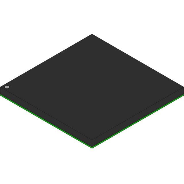
- Part No.:
- MCF5470VR200
- Manufacturer:
- NXP Semiconductors
- Category:
- Microcontrollers
- Package:
- 388-BBGA
- Datasheet:
-
 MCF5470VR200.pdf
- Description:
- IC MCU 32BIT ROMLESS 388PBGA
- Quantity:
- Payment:

- Shipping:

Inventory:1,780
Please send an inquiry. Send us your inquiry, and we will respond immediately.
Product details
Overview
MCF5470VR200 from Freescale Semiconductor is a ColdFire V4e-core microprocessor designed for high-performance embedded networking and industrial control applications. It operates at up to 200 MHz core frequency (312 MIPS @ 200 MHz), integrates a 32-Kbyte instruction cache, 32-Kbyte data cache, MMU, FPU compliant with IEEE-754 double-precision, and supports DDR/SDR SDRAM up to 1 GB via four chip selects.
For engineers reviewing the MCF5470VR200 datasheet, MCF5470VR200 pinout, MCF5470VR200 application, or MCF5470VR200 equivalent, key selection considerations include its 388-pin TEPBGA package, 1.5V core/2.5V DDR/3.3V I/O voltage domains, integrated dual 10/100 Mbps FECs with 2-Kbyte FIFOs per channel, USB 2.0 device controller with PHY, and PCI 2.2 interface supporting 33–66 MHz operation.
Technical Context
The MCF5470VR200 implements a limited superscalar ColdFire V4e core with Harvard architecture, separate 32-entry fully associative instruction and data translation lookahead buffers, and an integrated floating-point unit. Its internal XLB bus arbiter enables high-performance split transactions between multiple masters including the CPU, DMA, and peripheral controllers.
It features a flexible multi-function external bus (FlexBus) operating at 33–66 MHz with six chip selects, a 32-bit DDR/SDR SDRAM controller supporting 66–133 MHz operation and built-in initialization/refresh, and a version 2.2 PCI interface supporting up to five external PCI masters with configurable bus-to-XLB divider ratios (1:1, 1:2, 1:4).
Key Specifications
| Parameter | Value and Actual Design Meaning |
|---|---|
| Core Architecture | ColdFire V4e limited superscalar processor with Harvard memory architecture and MMU |
| Max Core Frequency | 200 MHz (312 MIPS Dhrystone 2.1), derived from 50 MHz CLKIN × 4 PLL multiplier |
| Memory Interfaces | 32-bit DDR/SDR SDRAM controller (66–133 MHz), FlexBus (33–66 MHz), PCI 2.2 (33–66 MHz) |
| On-chip Memory | 32-Kbyte instruction cache, 32-Kbyte data cache, 32-Kbyte system SRAM |
| I/O Voltage Domains | 1.5V core logic (IVDD), 2.5V DDR I/O (SDVDD), 3.3V PCI/FlexBus/USB I/O (EVDD) |
| Peripherals | Dual 10/100 Mbps FECs, USB 2.0 device controller with integrated PHY, four PSCs, I²C, DSPI, cryptography accelerator |
| Package | TEPBGA–388, 27 mm × 27 mm, 1.27 mm ball pitch |
Pinout & Package
Package: TEPBGA–388, 27 mm × 27 mm, 1.27 mm ball pitch, RoHS-compliant.
| Pin/Terminal | Circuit Role | Design Meaning |
|---|---|---|
| CLKIN | External reference clock input | Accepts 30–66.67 MHz crystal or oscillator; feeds PLL for core, XLB, and SDRAM clocks |
| RSTI | Asynchronous reset input | Active-low signal that initializes all internal logic and registers; synchronized internally to CLKIN |
| SDCS[3:0] | SDRAM chip select outputs | Four independent enables for up to 1 GB address space across DDR/SDR SDRAM devices |
| FBCS[5:0] | FlexBus chip select outputs | Six programmable enables for glueless interfacing to boot ROM, SRAM, or peripherals |
| PCIAD[31:0] | PCI address/data multiplexed bus | 32-bit bidirectional multiplexed address/data lines supporting PCI target/initiator operation |
| USBD+/USBD− | USB 2.0 differential data pair | Full-speed/high-speed differential signaling interface with integrated transceiver and 90Ω impedance routing requirement |
| FEC1_TXD[3:0]/FEC1_RXD[3:0] | Fast Ethernet MAC data interface | Two independent 4-bit nibble interfaces per FEC channel, each with dedicated 2-Kbyte FIFO |
Key Features
| Feature | Design Value |
|---|---|
| Floating-point unit (FPU) | IEEE-754 double-precision compliant with eight 64-bit registers, enabling deterministic real-time math in control algorithms |
| Dual Fast Ethernet Controllers (FECs) | Each supports MII/RMII, 2-Kbyte TX/RX FIFOs, and hardware checksum offload-reducing host CPU load in networked gateways |
| Integrated USB 2.0 Device Controller | Supports control/bulk/isochronous transfers with 4-Kbyte shared endpoint FIFO and integrated PHY-eliminating external transceiver need |
| Cryptography Accelerator | Hardware execution units for AES, DES/3DES, RC4, MD5/SHA-1/SHA-256, HMAC, and RNG-accelerating secure boot and TLS stack operations |
| System Integration Unit (SIU) | Includes interrupt controller, watchdog timer, two 32-bit slice timers, four 32-bit GP timers with PWM/compare, and GPIO multiplexing-centralizing system-level timing and I/O control |
Applications
| Industrial Ethernet Gateway | Secure Network Appliance |
|---|---|
Use Scenario: Protocol translation between Modbus TCP and EtherNet/IP in factory automation systems. IC Role / Device Role / Timing Role: Primary application processor executing real-time OS, managing dual FECs for concurrent LAN/WAN traffic, and running fieldbus protocol stacks. Use Value: Integrated MMU and FPU enable deterministic task scheduling and motion control math; dual FECs with 2-Kbyte FIFOs prevent packet loss under bursty industrial traffic. | Use Scenario: Firewall or VPN termination node in edge infrastructure with encrypted tunnel management. IC Role / Device Role / Timing Role: Host processor for Linux-based security stack, leveraging hardware crypto accelerator for AES-256 and SHA-256 operations. Use Value: Dedicated crypto engine offloads >90% of encryption cycles from CPU, sustaining 45 Mbps IPsec throughput without compromising application responsiveness. |
| Medical Imaging Control Unit | Telecom Base Station Controller |
Use Scenario: Real-time image acquisition and preprocessing in portable ultrasound systems. IC Role / Device Role / Timing Role: High-throughput data mover coordinating DDR SDRAM, PSCs for sensor interfaces, and USB 2.0 for image export. Use Value: 32-Kbyte caches and 200 MHz core deliver low-latency pixel processing; USB 2.0 device mode enables direct PC connection for DICOM file transfer. | Use Scenario: Remote radio head (RRH) controller managing CPRI over SFP+ and backhaul via Gigabit Ethernet. IC Role / Device Role / Timing Role: System controller interfacing FPGA baseband processor via FlexBus while handling OAM traffic via FEC and USB diagnostics. Use Value: FlexBus supports 66 MHz synchronous access to FPGA register space; PCI 2.2 interface enables optional expansion for additional PHY or timing modules. |
Equivalent & Alternatives
The following parts are listed as comparable options for similar microprocessor applications.
| Alternative Part | Technical Difference | Application Difference | Selection Advice |
|---|---|---|---|
| MCF5475VR266 | Higher core frequency (266 MHz), same package and peripheral set; requires 66.67 MHz CLKIN and tighter power sequencing | Targeted at bandwidth-intensive applications like video analytics where 312→410 MIPS uplift justifies thermal/power cost | Select when sustained compute throughput exceeds MCF5470VR200's 312 MIPS ceiling and board layout accommodates higher thermal dissipation |
| MPC8313EVRAGDB | PowerPC e300 core, 333 MHz, DDR2 controller, SEC crypto, but no integrated USB PHY or FECs-requires external PHYs | Designed for Linux-capable communications processors where PCIe and SATA are prioritized over USB/FEC integration | Choose when PCIe root complex or SATA host support is mandatory and external component count is acceptable for USB/Ethernet |
Compared with MCF5470VR200, MCF5475VR266 delivers +26% peak MIPS within identical footprint and software compatibility, while MPC8313EVRAGDB trades integrated USB/FEC for PCIe/SATA and PowerPC toolchain alignment-making it suitable for different OS and expansion priorities.
Availability
MCF5470VR200 is available at Aetrix Electronics and suitable for industrial Ethernet gateways, secure network appliances, medical imaging control units, and telecom base station controllers requiring stable component supply across extended product lifecycles.
Supply support for MCF5470VR200 includes scheduled delivery planning, volume procurement assistance, BOM continuity management, traceable sourcing, and lifecycle availability coordination for OEM customers, industrial embedded developers, connected-device designers, and electronics production programs.
Manufacturer
Freescale Semiconductor (now part of NXP Semiconductors) is a fabless semiconductor company specializing in embedded processing, analog, and connectivity solutions for automotive, industrial, and networking markets.
The MCF5470VR200 belongs to the ColdFire V4e microprocessor family, engineered for deterministic real-time performance in resource-constrained networking and control systems with integrated security and high-bandwidth memory interfaces.
FAQ
What is the maximum operating junction temperature for the MCF5470VR200?
The MCF5470VR200 has a maximum operating junction temperature of 105°C, as specified in the Freescale MCF547x datasheet Rev. 4. This limit must be maintained under all operating conditions-including worst-case ambient temperature, power dissipation, and PCB thermal design-to ensure reliable long-term operation. Thermal resistance θJMA for the 388-pin TEPBGA package is 19°C/W under natural convection on a four-layer board.
Does the MCF5470VR200 support both DDR and SDR SDRAM simultaneously?
No, the MCF5470VR200 SDRAM controller supports either DDR or SDR SDRAM-not both simultaneously. The mode is selected at boot time via configuration registers, and the I/O drivers are programmable for SSTL2 (DDR) or SSTL3 (SDR) drive strength. External memory topology must be homogeneous: one bank of DDR SDRAM or one bank of SDR SDRAM, up to 1 GB total across four chip selects.
What are the power supply sequencing requirements for the MCF5470VR200?
The MCF5470VR200 requires strict voltage sequencing: IVDD/PLL VDD and EVDD/SD VDD must track up to 0.9V during power-up, then separate to final values (1.5V core, 3.3V I/O, 2.5V DDR). IVDD must never exceed EVDD or SD VDD by more than 0.4V at any time. During power-down, IVDD/PLL VDD must drop to 0V before EVDD/SD VDD. Rise/fall times must be slower than 1 µs to avoid ESD diode conduction.
How many USB endpoints does the MCF5470VR200 support, and what types are configurable?
The MCF5470VR200 USB 2.0 device controller supports one control endpoint and six programmable endpoints, which can be independently configured as interrupt, bulk, or isochronous. Endpoint descriptors and 4-Kbyte shared FIFO RAM are managed by hardware, enabling simultaneous audio streaming (isochronous), HID reporting (interrupt), and firmware updates (bulk) without CPU intervention-critical for real-time USB device applications using MCF5470VR200.
Is the MCF5470VR200 pin-compatible with other MCF547x family members like MCF5472 or MCF5474?
Yes, the MCF5470VR200 is pin-compatible with all MCF547x variants (MCF5471–MCF5475) in the 388-pin TEPBGA package. Differences are limited to speed grade (e.g., 200 MHz vs. 266 MHz), enabled peripherals (e.g., crypto accelerator optional), and minor electrical specs-allowing drop-in replacement in existing designs when thermal and power delivery constraints permit the higher-frequency variant.
MCF5470VR200 Specifications
- Product attributes
- Attribute value
- Manufacturer:
- NXP Semiconductors
- Package/Case:
- 388-BBGA
- Series:
- MCF547x
- Packaging:
- Tray
- Product Status:
- Not For New Designs
- Programmable:
- Not Verified
- Core Processor:
- Coldfire V4E
- Core Size:
- 32-Bit Single-Core
- Speed:
- 200MHz
- Connectivity:
- EBI/EMI, Ethernet, I2C, SPI, UART/USART, USB
- Peripherals:
- DMA, PWM, WDT
- Number of I/O:
- 99
- Program Memory Size:
- -
- Program Memory Type:
- ROMless
- EEPROM Size:
- -
- RAM Size:
- 32K x 8
- Voltage - Supply (Vcc/Vdd):
- 1.43V ~ 1.58V
- Data Converters:
- -
- Oscillator Type:
- External
- Operating Temperature:
- 0°C ~ 70°C (TA)
- Grade:
- -
- Qualification:
- -
- Mounting Type:
- Surface Mount
- Supplier Device Package:
MCF5470VR200 FAQ
1.How can I place an order for MCF5470VR200 through Aetrix?
Please submit a Request for Quotation (RFQ) for MCF5470VR200 on Aetrix. Our sales agent will provide a competitive quotation and guide you through the order confirmation once you accept the terms.
2.Are the price and stock information for MCF5470VR200 reliable?
The price and inventory of MCF5470VR200 are updated periodically and may fluctuate due to market conditions. Stock and pricing data are typically refreshed every 24 hours. Quotation validity for MCF5470VR200 is usually 5 days.
3.What payment methods are accepted for MCF5470VR200?
We accept Wire Transfer, PayPal, Credit Card, Western Union, MoneyGram, and Escrow for MCF5470VR200 transactions.
Note: Certain payment methods may incur a processing fee.
4.How is shipping managed for MCF5470VR200?
MCF5470VR200 orders can be shipped via leading logistics carriers, including DHL, UPS, FedEx, TNT, or Registered Mail.
Once your MCF5470VR200 order is processed, you will receive an email with the shipment details and tracking number.
Note: Tracking information may take up to 24 hours to appear. Express delivery typically takes 3–5 business days.
5.How can I obtain technical support or documentation for MCF5470VR200?
For technical support, including MCF5470VR200 datasheets, pinout diagrams, or application guidance, please contact our engineering support team. They can provide detailed documentation and assistance for your MCF5470VR200 requirements.
6.How does Aetrix verify that MCF5470VR200 is sourced from the original manufacturer or authorized distributors?
All MCF5470VR200 products on Aetrix are procured from qualified distributors and authorized channels. Our dedicated quality assurance team conducts strict verification, including traceability checks and, if necessary, third-party testing. This ensures that MCF5470VR200 meets industry standards.
7.What is the process for return or replacement of MCF5470VR200?
All MCF5470VR200 units undergo pre-shipment inspection (PSI). If there is an issue with MCF5470VR200, returns or replacements are accepted under the following conditions:
1.Quantity discrepancies, incorrect items, or visible external defects (such as breakage or corrosion), acknowledged by Aetrix.
2.The issue is reported within 90 days of delivery.
3.The MCF5470VR200 part is unused and in its original packaging.
Return procedure for MCF5470VR200:
1.Submit a request within 90 days.
2.Obtain a Return Material Authorization (RMA) from Aetrix.
MCF5470VR200 Tags

-
ATTINY4-TSHR
Microchip Technology
-
ATTINY10-TSHR
Microchip Technology
-
ATTINY10-TS8R
Microchip Technology

-
ATTINY202-SSNR
Microchip Technology
-
ATTINY202-SSFR
Microchip Technology
-
ATTINY402-SSNR
Microchip Technology

-
PIC16F15213T-I/MF
Microchip Technology
-
PIC16F15213-E/MF
Microchip Technology

-
PIC10F200T-I/OT
Microchip Technology
-
ATTINY412-SSNR
Microchip Technology
-
PIC10F202T-I/OT
Microchip Technology

-
ATTINY404-SSNR
Microchip Technology
Tech Hub

A practical engineering guide to 3.3V and 5V logic compatibility, input thresholds, resistor dividers, translator ICs, MOSFET level shifting, I2C pull-ups, timing limits and power-sequencing risks.

The 74HC595 uses push-pull logic outputs, while the TPIC6B595 uses 50 V open-drain DMOS sinks for higher-power loads. This guide compares timing, current limits, 3.3 V interfacing, load wiring, thermal…

The 74HC595 converts serial data into eight stable parallel outputs. This guide covers pin functions, shift and storage timing, OE and MR behavior, drive-current limits, cascading, voltage compatibilit…

A technical comparison of level-sensitive latches and edge-triggered flip-flops, covering timing windows, setup and hold limits, master–slave operation, time borrowing, race-through, HDL inference and…

A D latch stores one bit while Enable controls when data can pass. This reference covers gate-level operation, truth tables, transparency, setup and hold timing, LE versus OE, common ICs and practical …

An SR latch stores one bit through cross-coupled feedback. This engineering reference covers NOR and NAND implementations, truth tables, forbidden-state recovery, gated operation, switch debouncing, fa…

Latch circuits retain one bit through feedback. This technical reference covers SR and D latches, truth tables, transparency, timing limits, latch-versus-flip-flop behavior, applications and common log…

An engineering guide to LED driver operation, constant-current and constant-voltage outputs, linear and switching topologies, dimming, IC selection, calculations, replacement compatibility, and fault c…

Operational amplifier guide covering op amp basics, feedback, ideal vs real op amps, common configurations, buffer circuits, offset, bias current, gain-bandwidth, slew rate, rail-to-rail limits and sel…

Jumper cables guide covering safe connection order, red and black clamp placement, final ground connection, cable gauge, length, clamp quality, copper vs CCA cables, jump starter comparison and battery…


