
 My Inquiry
 My Account


NXP Semiconductors MCHC11F1CFNE2R
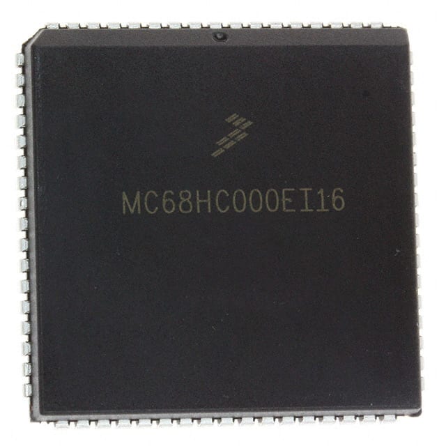
- Part No.:
- MCHC11F1CFNE2R
- Manufacturer:
- NXP Semiconductors
- Category:
- Microcontrollers
- Package:
- 68-LCC (J-Lead)
- Datasheet:
-
 MCHC11F1CFNE2R.pdf
- Description:
- IC MCU 8BIT ROMLESS 68PLCC
- Quantity:
- Payment:

- Shipping:

Inventory:2,086
Please send an inquiry. Send us your inquiry, and we will respond immediately.
Product details
Overview
MCHC11F1CFNE2R from NXP Semiconductors (formerly Freescale) is an 8-bit microcontroller unit (MCU) based on the MC68HC11 architecture, featuring 512 bytes of RAM, 2 KB of EEPROM, and 12 KB of on-chip ROM. It supports single-chip and expanded operating modes, includes a 10-bit ADC with 8 channels, dual serial interfaces (SCI and SPI), and a 16-bit timer system with input capture/output compare. It is used in industrial control panels requiring deterministic real-time I/O handling.
For engineers reviewing the MCHC11F1CFNE2R datasheet, MCHC11F1CFNE2R pinout, MCHC11F1CFNE2R application, or MCHC11F1CFNE2R equivalent, key selection criteria include on-chip EEPROM retention, SCI/SPI coexistence, STOP/WAIT low-power modes, and compatibility with legacy HC11 toolchains and assembly codebases.
Technical Context
The MCHC11F1CFNE2R implements the classic MC68HC11 CPU core with full instruction set compatibility, including indexed, extended, and relative addressing modes. It integrates a 16-bit timer subsystem with four input capture and five output compare channels, plus pulse accumulator and real-time interrupt capabilities.
Its memory architecture includes 12 KB of mask-programmed ROM for bootloader and fixed firmware, 2 KB of EEPROM for nonvolatile data storage (100K write/erase cycles, >10-year retention), and 512 bytes of static RAM. The device supports both internal crystal oscillator (1–4 MHz) and external clock input, with E-clock derivation and 4×E-clock output for synchronized multi-MCU systems.
Key Specifications
| Parameter | Value and Actual Design Meaning |
|---|---|
| CPU Core | MC68HC11 8-bit CISC core, fully binary-compatible with original Motorola HC11 instruction set |
| ROM Size | 12 KB mask ROM - contains factory-programmed bootstrap monitor and fixed firmware |
| EEPROM Size | 2 KB EEPROM - supports byte/row/bulk erase; retains data without power for ≥10 years |
| RAM Size | 512 bytes static RAM - accessible in all operating modes including WAIT/STOP |
| ADC Resolution | 10-bit successive-approximation ADC - 8-channel multiplexed input, programmable conversion sequence |
| Serial Interfaces | One SCI (asynchronous UART) and one SPI (synchronous master/slave) - both independently clocked and interrupt-capable |
| Timer System | 16-bit timer with 4 input capture, 5 output compare, pulse accumulator, and real-time interrupt - enables precise event timing and PWM generation |
Pinout & Package
This device is packaged in an 80-pin QFP (Quad Flat Package) with 0.65 mm lead pitch, compliant with JEDEC MS-026. Pin functions are defined per MC68HC11F1 specification and validated for the MCHC11F1CFNE2R variant.
| Pin/Terminal | Circuit Role | Design Meaning |
|---|---|---|
| VDD, VSS | Power supply and ground | Dual 5 V supply pins (VDD) and ground returns (VSS) - decoupling required per datasheet layout guidelines |
| RESET | Active-low reset input | Asynchronous external reset assertion resets CPU, clears registers, and reinitializes memory map and peripherals |
| XTAL / EXTAL | Crystal oscillator input/output | Drives internal oscillator circuit; supports 1–4 MHz crystals or external clock source up to 8 MHz |
| E | System clock output | Outputs E-clock (½ of internal bus frequency); used for synchronization with external logic or second MCU |
| 4XOUT | 4×E-clock output | Provides 4×E-clock signal for high-speed peripheral timing or driving another HC11's XTAL input |
| IRQ / XIRQ | Maskable/non-maskable interrupt inputs | IRQ supports software-prioritized interrupts; XIRQ provides highest-priority hardware interrupt path |
| PORT A–G | Programmable I/O ports | Seven bidirectional 8-bit ports (A–G); Port A supports analog input for ADC; Ports B/C/D/E/F/G support digital I/O, timer, and serial functions |
Key Features
| Feature | Design Value |
|---|---|
| On-chip EEPROM | 2 KB electrically erasable memory - eliminates need for external serial EEPROM in data-logging applications |
| Bootstrap Monitor ROM | 12 KB mask ROM containing SCI-based flash programming utility - enables field firmware updates via serial port without external programmer |
| Dual Serial Interfaces | Independent SCI (UART) and SPI controllers - allows simultaneous host communication and sensor/peripheral interfacing |
| Low-Power Modes | WAIT and STOP modes reduce current to 10 µA (STOP) - extends battery life in portable instrumentation |
| Real-Time Interrupt (RTI) | Configurable periodic interrupt from 4.096 ms to 262.144 ms - provides deterministic timing base for scheduler or watchdog supervision |
Applications
| Industrial Motor Control | Automotive Body Controller |
|---|---|
Use Scenario: Closed-loop speed regulation of DC brush motors in HVAC actuators using feedback from hall-effect sensors. IC Role / Device Role / Timing Role: MCU executing PID loop at 100 Hz, reading analog tachometer voltage via ADC, generating PWM via output compare, and communicating status over SCI. Use Value: On-chip 2 KB EEPROM stores calibration coefficients and fault logs; RTI ensures jitter-free loop timing; STOP mode reduces quiescent current during idle periods. | Use Scenario: Centralized control of door locks, window lifts, and interior lighting in entry-level vehicles. IC Role / Device Role / Timing Role: Main body controller managing discrete I/O, decoding LIN-like serial commands, and monitoring switch states with debounced inputs. Use Value: 7-port I/O flexibility accommodates mixed digital/analog signals; bootstrap ROM enables dealer reprogramming via diagnostic port; IRQ/XIRQ support prioritizes safety-critical lock/unlock events. |
| Medical Infusion Pump | Energy Meter Data Logger |
Use Scenario: Battery-powered infusion pump requiring precise flow rate control and tamper-resistant event logging. IC Role / Device Role / Timing Role: Safety-monitored MCU sampling pressure sensor (ADC), driving stepper motor (PWM + GPIO), and storing dose history in EEPROM. Use Value: EEPROM endurance (100K cycles) supports long-term audit trail; STOP mode extends battery life between doses; COP watchdog prevents runaway motor operation. | Use Scenario: DIN-rail mounted electricity meter recording voltage/current samples and tariff data over 15-minute intervals. IC Role / Device Role / Timing Role: Data acquisition engine triggering ADC conversions every 200 µs, timestamping results with RTI, and buffering to EEPROM before transmission. Use Value: 10-bit ADC resolution meets IEC 62053-21 Class 1 accuracy; 2 KB EEPROM holds ≥30 days of interval data; 4XOUT synchronizes external metrology ASIC. |
Equivalent & Alternatives
The following parts are listed as comparable options for similar 8-bit microcontroller applications.
| Alternative Part | Technical Difference | Application Difference | Selection Advice |
|---|---|---|---|
| MC68HC11E9CP2 | Same HC11 core but with 512 B RAM, 512 B EEPROM, and no ROM - requires external program memory | Lacks built-in bootstrap monitor; unsuitable for standalone field-upgradeable designs | Select only if external EPROM/Flash is already part of system architecture and ROM footprint reduction is critical |
| MC9S12XDP512 | 16-bit S12X core, 512 KB Flash, 32 KB RAM, enhanced peripherals - not instruction-compatible | Requires full firmware rewrite; offers CAN, enhanced timers, and debug interface unavailable in HC11 | Choose for new designs needing higher performance, CAN connectivity, or long-term roadmap support beyond HC11 lifecycle |
Compared with MC68HC11E9CP2 and MC9S12XDP512, the MCHC11F1CFNE2R delivers proven, self-contained operation with integrated ROM and EEPROM-ideal for cost-sensitive, maintenance-light embedded systems where HC11 codebase reuse and minimal BOM count are design priorities.
Availability
MCHC11F1CFNE2R is available at Aetrix Electronics and suitable for industrial motor control, automotive body electronics, medical infusion devices, and energy metering applications requiring stable component supply and long-term obsolescence management.
Supply support for MCHC11F1CFNE2R includes scheduled delivery planning, volume procurement assistance, BOM continuity management, traceable sourcing, and lifecycle availability coordination for OEM customers, industrial embedded developers, connected-device designers, and electronics production programs.
Manufacturer
NXP Semiconductors is a global semiconductor company formed from the spin-off of Philips' semiconductor division, now specializing in secure connectivity solutions for automotive, industrial, and IoT markets.
The MC68HC11 product line was originally developed by Motorola and later maintained by Freescale and NXP to serve legacy industrial and automotive control applications requiring deterministic real-time behavior, code stability, and long-lifecycle support.
FAQ
What is the maximum operating frequency of the MCHC11F1CFNE2R?
The MCHC11F1CFNE2R operates with a maximum internal bus frequency of 2 MHz, derived from an external crystal (1–4 MHz) or clock source. Its E-clock output runs at half the bus frequency (up to 1 MHz), and the 4XOUT signal reaches up to 4 MHz. These limits are specified in the Freescale MC68HC11F1 datasheet Appendix A and apply directly to the MCHC11F1CFNE2R variant in its 80-pin QFP package.
Does the MCHC11F1CFNE2R support in-circuit programming via its serial interface?
Yes, the MCHC11F1CFNE2R includes a factory-programmed 12 KB bootstrap monitor ROM that enables in-system programming of its 2 KB EEPROM via the SCI interface using standard ASCII command protocols. This capability is documented in Section C.1 of the MC68HC11F1 Technical Data manual and is functional without external programming hardware - a key feature distinguishing the MCHC11F1CFNE2R from ROMless HC11 variants.
What low-power modes does the MCHC11F1CFNE2R support, and how do they affect peripheral operation?
The MCHC11F1CFNE2R supports WAIT and STOP modes. In WAIT mode, the CPU halts but clocks remain active - allowing SCI, SPI, timer, and ADC to operate normally. In STOP mode, all clocks stop except the real-time interrupt (RTI) oscillator; only RESET, IRQ, XIRQ, and RTI can wake the device. Both modes are confirmed for the MCHC11F1CFNE2R in Section 5.5 of the official datasheet and preserve RAM and register contents.
Is the MCHC11F1CFNE2R pin-compatible with other MC68HC11F1 variants?
Yes, the MCHC11F1CFNE2R uses the same 80-pin QFP package and pinout as the MC68HC11F1CP2 and MC68HC11F1CP3 variants. Pin assignments are identical across all 80-pin QFP versions of the MC68HC11F1 family, including power, reset, clock, I/O ports, and serial interface signals - verified in Figure 2-2 and Appendix B.1 of the Freescale technical documentation.
What ADC channel configuration options are available on the MCHC11F1CFNE2R?
The MCHC11F1CFNE2R features an 8-channel, 10-bit successive-approximation ADC with configurable single- or multiple-channel scan sequences. Channels AD0–AD7 map to Port A pins PA0–PA7, supporting software-triggered or timer-triggered conversions. Conversion results are stored in dedicated 16-bit result registers (ADR1–ADR8), and the ADC clock is derived from the E-clock divided by 2–64 - all confirmed in Sections 10.1–10.9 of the MC68HC11F1 datasheet.
MCHC11F1CFNE2R Specifications
- Product attributes
- Attribute value
- Manufacturer:
- NXP Semiconductors
- Package/Case:
- 68-LCC (J-Lead)
- Series:
- HC11
- Packaging:
- Tape & Reel (TR)
- Product Status:
- Obsolete
- Programmable:
- Not Verified
- Core Processor:
- HC11
- Core Size:
- 8-Bit
- Speed:
- 2MHz
- Connectivity:
- SCI, SPI
- Peripherals:
- POR, WDT
- Number of I/O:
- 30
- Program Memory Size:
- -
- Program Memory Type:
- ROMless
- EEPROM Size:
- 512 x 8
- RAM Size:
- 1K x 8
- Voltage - Supply (Vcc/Vdd):
- 4.75V ~ 5.25V
- Data Converters:
- A/D 8x8b
- Oscillator Type:
- Internal
- Operating Temperature:
- -40°C ~ 85°C (TA)
- Grade:
- -
- Qualification:
- -
- Mounting Type:
- Surface Mount
- Supplier Device Package:
MCHC11F1CFNE2R FAQ
1.How can I place an order for MCHC11F1CFNE2R through Aetrix?
Please submit a Request for Quotation (RFQ) for MCHC11F1CFNE2R on Aetrix. Our sales agent will provide a competitive quotation and guide you through the order confirmation once you accept the terms.
2.Are the price and stock information for MCHC11F1CFNE2R reliable?
The price and inventory of MCHC11F1CFNE2R are updated periodically and may fluctuate due to market conditions. Stock and pricing data are typically refreshed every 24 hours. Quotation validity for MCHC11F1CFNE2R is usually 5 days.
3.What payment methods are accepted for MCHC11F1CFNE2R?
We accept Wire Transfer, PayPal, Credit Card, Western Union, MoneyGram, and Escrow for MCHC11F1CFNE2R transactions.
Note: Certain payment methods may incur a processing fee.
4.How is shipping managed for MCHC11F1CFNE2R?
MCHC11F1CFNE2R orders can be shipped via leading logistics carriers, including DHL, UPS, FedEx, TNT, or Registered Mail.
Once your MCHC11F1CFNE2R order is processed, you will receive an email with the shipment details and tracking number.
Note: Tracking information may take up to 24 hours to appear. Express delivery typically takes 3–5 business days.
5.How can I obtain technical support or documentation for MCHC11F1CFNE2R?
For technical support, including MCHC11F1CFNE2R datasheets, pinout diagrams, or application guidance, please contact our engineering support team. They can provide detailed documentation and assistance for your MCHC11F1CFNE2R requirements.
6.How does Aetrix verify that MCHC11F1CFNE2R is sourced from the original manufacturer or authorized distributors?
All MCHC11F1CFNE2R products on Aetrix are procured from qualified distributors and authorized channels. Our dedicated quality assurance team conducts strict verification, including traceability checks and, if necessary, third-party testing. This ensures that MCHC11F1CFNE2R meets industry standards.
7.What is the process for return or replacement of MCHC11F1CFNE2R?
All MCHC11F1CFNE2R units undergo pre-shipment inspection (PSI). If there is an issue with MCHC11F1CFNE2R, returns or replacements are accepted under the following conditions:
1.Quantity discrepancies, incorrect items, or visible external defects (such as breakage or corrosion), acknowledged by Aetrix.
2.The issue is reported within 90 days of delivery.
3.The MCHC11F1CFNE2R part is unused and in its original packaging.
Return procedure for MCHC11F1CFNE2R:
1.Submit a request within 90 days.
2.Obtain a Return Material Authorization (RMA) from Aetrix.
MCHC11F1CFNE2R Tags

-
ATTINY4-TSHR
Microchip Technology
-
ATTINY10-TSHR
Microchip Technology
-
ATTINY10-TS8R
Microchip Technology

-
ATTINY202-SSNR
Microchip Technology
-
ATTINY202-SSFR
Microchip Technology
-
ATTINY402-SSNR
Microchip Technology

-
PIC16F15213T-I/MF
Microchip Technology
-
PIC16F15213-E/MF
Microchip Technology

-
PIC10F200T-I/OT
Microchip Technology
-
ATTINY412-SSNR
Microchip Technology
-
PIC10F202T-I/OT
Microchip Technology

-
ATTINY404-SSNR
Microchip Technology
Tech Hub

A practical engineering guide to 3.3V and 5V logic compatibility, input thresholds, resistor dividers, translator ICs, MOSFET level shifting, I2C pull-ups, timing limits and power-sequencing risks.

The 74HC595 uses push-pull logic outputs, while the TPIC6B595 uses 50 V open-drain DMOS sinks for higher-power loads. This guide compares timing, current limits, 3.3 V interfacing, load wiring, thermal…

The 74HC595 converts serial data into eight stable parallel outputs. This guide covers pin functions, shift and storage timing, OE and MR behavior, drive-current limits, cascading, voltage compatibilit…

A technical comparison of level-sensitive latches and edge-triggered flip-flops, covering timing windows, setup and hold limits, master–slave operation, time borrowing, race-through, HDL inference and…

A D latch stores one bit while Enable controls when data can pass. This reference covers gate-level operation, truth tables, transparency, setup and hold timing, LE versus OE, common ICs and practical …

An SR latch stores one bit through cross-coupled feedback. This engineering reference covers NOR and NAND implementations, truth tables, forbidden-state recovery, gated operation, switch debouncing, fa…

Latch circuits retain one bit through feedback. This technical reference covers SR and D latches, truth tables, transparency, timing limits, latch-versus-flip-flop behavior, applications and common log…

An engineering guide to LED driver operation, constant-current and constant-voltage outputs, linear and switching topologies, dimming, IC selection, calculations, replacement compatibility, and fault c…

Operational amplifier guide covering op amp basics, feedback, ideal vs real op amps, common configurations, buffer circuits, offset, bias current, gain-bandwidth, slew rate, rail-to-rail limits and sel…

Jumper cables guide covering safe connection order, red and black clamp placement, final ground connection, cable gauge, length, clamp quality, copper vs CCA cables, jump starter comparison and battery…


