
 My Inquiry
 My Account


NXP Semiconductors MCIMX257CVM4
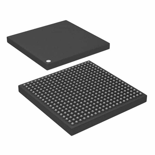
- Part No.:
- MCIMX257CVM4
- Manufacturer:
- NXP Semiconductors
- Category:
- Microprocessors
- Package:
- 400-LFBGA
- Datasheet:
-
 MCIMX257CVM4.pdf
- Description:
- IC MPU I.MX25 400MHZ 400LFBGA
- Quantity:
- Payment:

- Shipping:

Inventory:3,676
Please send an inquiry. Send us your inquiry, and we will respond immediately.
Product details
Overview
MCIMX257CVM4 from NXP Semiconductors (formerly Freescale) is an industrial-grade ARM926EJ-S applications processor operating at 400 MHz, integrating 128 KB on-chip SRAM, dual USB PHYs (HS OTG + FS Host), 10/100 Ethernet MAC, LCD controller with alpha blending, and touchscreen ADC-designed for HMI panels, patient monitors, and residential gateways.
For engineers reviewing the MCIMX257CVM4 datasheet, MCIMX257CVM4 pinout, MCIMX257CVM4 application, or MCIMX257CVM4 equivalent, key selection criteria include its –40°C to +85°C extended temperature rating, 17×17 mm 0.8 mm pitch MAPBGA-400 package, support for DDR2 up to 133 MHz, and integrated security features including DryIce tamper detection and secure boot.
Technical Context
The MCIMX257CVM4 implements a single ARM926EJ-S core with 16 KB L1 instruction and 16 KB L1 data cache, running at up to 400 MHz under 1.38–1.52 V core supply. It integrates a Smart DMA (SDMA) engine with 32 channels, two eSDHC controllers supporting SD/SDIO/MMC in 1-/4-/8-bit modes, and a dedicated CCM module managing wait/stop/doze low-power states via clock gating.
Its peripheral set includes FlexCAN v2.0 (2 channels), ESAI for full-duplex audio, CSI for CMOS image sensors, SIM interfaces compliant with ISO7816 for smart cards, and a 12-bit ADC with integrated resistive touchscreen controller-enabling simultaneous analog measurement and touch coordinate acquisition without external components.
Key Specifications
| Parameter | Value and Actual Design Meaning |
|---|---|
| CPU Core | ARM926EJ-S, 400 MHz max - enables real-time deterministic execution of Linux-based HMI firmware with Java or Qt acceleration. |
| On-chip Memory | 128 KB SRAM - eliminates need for external RAM in RTOS-based medical devices requiring ultra-low-power LCD refresh. |
| Memory Interface | DDR2 up to 133 MHz - supports 16-bit wide DDR2 SDRAM for high-bandwidth framebuffer storage in color TFT displays. |
| USB Integration | HS USB 2.0 OTG + FS USB Host PHY - enables direct connection to USB peripherals (keyboards, flash drives) and host-mode device enumeration without external transceivers. |
| Security Features | DryIce module with RTC, volatile key storage, and MESH_C/MESH_D tamper detect - provides hardware-enforced secure boot and time-stamped DRM for smart metering applications. |
| Operating Temperature | –40°C to +85°C - qualified for industrial control panels deployed in unconditioned environments like factory floors or outdoor utility enclosures. |
| Package | MAPBGA-400, 17×17 mm, 0.8 mm pitch - compatible with standard PCB assembly processes and thermal vias for passive heat dissipation in fanless designs. |
Pinout & Package
MCIMX257CVM4 uses a 400-ball MAPBGA package (Case 5284), 17 mm × 17 mm, 0.8 mm pitch, with ball map defined in Table 103 of IMX25CEC Rev. 10. Power delivery includes dedicated QVDD (core), NVDD_GPIO1/2 (I/O banks), NVDD_DDR2 (memory), and NVCC_DRYICE (security domain). Signal balls are grouped into functional banks: EMI (DDR2/NAND/NOR), USBPHY1/2, FEC, CSI, LCDC, and IOMUX-configurable GPIOs.
| Pin/Terminal | Circuit Role | Design Meaning |
|---|---|---|
| BAT_VDD | DryIce backup supply input | Must be connected to coin cell (1.15–1.55 V) to retain RTC and cryptographic keys during main power loss. |
| NVCC_DRYICE | DryIce regulated output | Supplies external tamper-detect circuitry; requires ≥4 µF capacitor to maintain voltage during power transitions. |
| MESH_C / MESH_D | Wire-mesh tamper detect inputs | Form active-high tamper loop: floating or shorting triggers immediate key erasure and RTC invalidation. |
| TAMPER_A / TAMPER_B | External tamper detect inputs | Asserted when pulled to NVCC_DRYICE; used for enclosure intrusion or cover-removal detection. |
| USBPHY1_DM / DP | High-speed USB differential pair | Impedance-controlled 10 Ω output; requires 33 Ω series resistors near pins for signal integrity per USB 2.0 spec. |
| OSC32K_EXTAL / XTAL | 32.768 kHz crystal interface | Analog pins for precision RTC timing; require 6–8 pF load capacitors and <7 pF shunt capacitance. |
Key Features
| Feature | Design Value |
|---|---|
| Advanced Power Management | Multiple low-power states (wait/stop/doze) controlled by CCM clock gating - reduces system idle power to <10 mW while preserving SRAM and RTC state. |
| Integrated Touchscreen Controller | 12-bit ADC with dedicated TSC block - supports 4-wire resistive touch panels with pressure-independent coordinate acquisition and auxiliary analog sensing (voltage/temp). |
| Flexible External Memory Support | EMI subsystem with WEIM (NOR/PSRAM), NFC (NAND), and ESDCTL (DDR2/SDR) - enables mixed-memory BOMs for cost-optimized industrial gateways. |
| Hardware Security Engine | DryIce + IIM fusebox - provides tamper-evident secure boot, encrypted key storage, and one-time programmable device identifiers for regulatory compliance. |
| Audio Subsystem | AUDMUX + ESAI + SSI - enables concurrent routing of voice, SPDIF, and I2S streams between codecs, DSPs, and internal peripherals without CPU overhead. |
Applications
| Industrial HMI Panels | Patient Monitoring Devices |
|---|---|
Use Scenario: Wall-mounted control interface in factory automation systems with graphical UI, real-time alarms, and local data logging. IC Role / Device Role / Timing Role: Central applications processor executing Linux with Qt-based GUI, driving 800×480 TFT via LCDC, polling sensors over I2C/UART, and communicating via Ethernet/FlexCAN. Use Value: Integrated 128 KB SRAM eliminates external RAM, reducing BOM count and board area; –40°C to +85°C rating ensures reliability in non-climate-controlled production lines. | Use Scenario: Portable bedside monitor acquiring ECG, SpO₂, and temperature, displaying waveforms, and transmitting alerts via Ethernet. IC Role / Device Role / Timing Role: Real-time data aggregator with 12-bit ADC for analog biosignals, LCDC for waveform rendering, FEC for HL7-over-Ethernet transmission, and DryIce for secure timestamping of clinical events. Use Value: On-chip touchscreen controller enables intuitive touch UI without external digitizer IC; battery-backed BAT_VDD preserves RTC across power cycles for audit-trail compliance. |
| Residential Smart Gateways | Handheld Scanners & Printers |
Use Scenario: Home energy management hub aggregating smart meter data, controlling HVAC/lighting, and hosting local web UI. IC Role / Device Role / Timing Role: Embedded Linux host with eSDHC for local storage, FEC for broadband backhaul, USB OTG for firmware updates, and SIM interface for cellular failover. Use Value: Dual USB PHYs allow simultaneous host (flash drive update) and device (PC configuration) operation; integrated security prevents unauthorized firmware injection. | Use Scenario: Battery-powered barcode scanner with OLED display, Bluetooth connectivity, and ruggedized casing. IC Role / Device Role / Timing Role: Low-power applications processor running FreeRTOS, scanning via CSI-connected imager, rendering UI on OLED via LCDC, and managing power states via CCM. Use Value: 400 MHz ARM926EJ-S delivers fast decode latency; 128 KB SRAM enables full firmware residency for instant wake-from-sleep response. |
Equivalent & Alternatives
The following parts are listed as comparable options for similar applications processor applications.
| Alternative Part | Technical Difference | Application Difference | Selection Advice |
|---|---|---|---|
| MCIMX253CVM4 | Lacks FlexCAN, ESAI, CSI, SIM, and touchscreen controller; identical CPU, SRAM, USB, Ethernet, and LCD controller. | Suitable for simpler HMI or gateway designs without automotive bus, advanced audio, or imaging requirements. | Select MCIMX253CVM4 when CAN, camera, or smart card interfaces are unnecessary-reduces software complexity and BOM cost. |
| i.MX6ULL G0 | ARM Cortex-A7 @ 900 MHz, 512 MB DDR3 support, GPU, newer security (CAAM), but no DryIce or MESH tamper detection. | Targets higher-performance UIs (e.g., animated dashboards) and modern Linux distributions; lacks legacy industrial tamper-hardening features. | Choose i.MX6ULL G0 for next-gen designs needing richer graphics and long-term roadmap support, accepting trade-off in physical tamper resistance. |
Compared with MCIMX257CVM4, MCIMX253CVM4 removes imaging and automotive interfaces while retaining identical core performance and industrial temperature range-making it ideal for cost-sensitive HMI-only use cases. The i.MX6ULL G0 offers higher CPU throughput and modern peripherals but sacrifices DryIce-level tamper detection and extended lifecycle availability for legacy industrial deployments.
Availability
MCIMX257CVM4 is available at Aetrix Electronics and suitable for industrial HMI panels, patient-monitoring devices, and residential smart gateways requiring stable component supply across multi-year production programs.
Supply support for MCIMX257CVM4 includes scheduled delivery planning, volume procurement assistance, BOM continuity management, traceable sourcing, and lifecycle availability coordination for OEM customers, industrial embedded developers, connected-device designers, and electronics production programs.
Manufacturer
NXP Semiconductors is a global semiconductor leader focused on secure connectivity solutions for automotive, industrial, and IoT markets, with roots in Freescale's embedded processor heritage.
The i.MX25 product line was designed specifically for cost-sensitive, power-constrained industrial and consumer embedded applications requiring robust security, rich multimedia, and extended temperature operation-targeting HMI, medical, and smart infrastructure.
FAQ
What is the maximum DDR2 memory speed supported by MCIMX257CVM4?
The MCIMX257CVM4 supports DDR2 memory at up to 133 MHz, corresponding to a 266 MT/s data rate in double-data-rate mode. This is specified in the Electrical Characteristics section (Table 8) of the IMX25CEC datasheet and enables sufficient bandwidth for 800×480 color TFT framebuffers with alpha blending enabled in the LCDC.
Does MCIMX257CVM4 include an integrated USB PHY?
Yes, MCIMX257CVM4 integrates both a high-speed USB 2.0 OTG PHY and a full-speed USB host PHY on-die. These eliminate the need for external transceivers and are electrically characterized per USB 2.0 specification, with USBPHY1_DM/DP requiring 33 Ω series termination and USBPHY2_DM/DP supporting standard FS signaling.
What security features are implemented in MCIMX257CVM4?
MCIMX257CVM4 includes DryIce (hardware RTC with tamper-detect inputs MESH_C/D and TAMPER_A/B), IIM fusebox for one-time programmable keys and chip IDs, secure boot enforcement, and hardware-accelerated encryption primitives. These features are documented in Sections 2 and 3 of IMX25CEC and enable FIPS-compliant secure boot and DRM in medical and utility applications.
Is MCIMX257CVM4 pin-compatible with other i.MX25 variants?
Yes, MCIMX257CVM4 shares the same 400-ball MAPBGA-400 package (17×17 mm, 0.8 mm pitch) and ball map (Table 103) with MCIMX253CVM4 and MCIMX258CVM4. Pin functions are consistent across these variants; differences lie only in enabled peripherals (e.g., FlexCAN, ESAI), not in physical layout or electrical signaling.
What is the purpose of the BAT_VDD pin on MCIMX257CVM4?
The BAT_VDD pin supplies backup power to the DryIce security module, ensuring retention of RTC time and cryptographic keys during main power loss. It must be connected to a coin cell (1.15–1.55 V) in security-critical applications like smart meters; in non-security use, it may be tied to QVDD per IMX25CEC Section 3.1.2.
MCIMX257CVM4 Specifications
- Product attributes
- Attribute value
- Manufacturer:
- NXP Semiconductors
- Package/Case:
- 400-LFBGA
- Series:
- i.MX25
- Packaging:
- Tray
- Product Status:
- Obsolete
- Core Processor:
- ARM926EJ-S
- Number of Cores/Bus Width:
- 1 Core, 32-Bit
- Speed:
- 400MHz
- Co-Processors/DSP:
- -
- RAM Controllers:
- LPDDR, DDR, DDR2
- Graphics Acceleration:
- No
- Display & Interface Controllers:
- Keypad, LCD, Touchscreen
- Ethernet:
- 10/100Mbps (1)
- SATA:
- -
- USB:
- USB 2.0 + PHY (2)
- Voltage - I/O:
- 2.0V, 2.5V, 2.7V, 3.0V, 3.3V
- Operating Temperature:
- -40°C ~ 85°C (TA)
- Grade:
- -
- Qualification:
- -
- Security Features:
- -
- Mounting Type:
- Surface Mount
- Supplier Device Package:
- 400-LFBGA (17x17)
- Additional Interfaces:
- CAN, I2C, I2S, MMC/SD/SDIO, SAI, SPI, SSI, SSP, UART
MCIMX257CVM4 FAQ
1.How can I place an order for MCIMX257CVM4 through Aetrix?
Please submit a Request for Quotation (RFQ) for MCIMX257CVM4 on Aetrix. Our sales agent will provide a competitive quotation and guide you through the order confirmation once you accept the terms.
2.Are the price and stock information for MCIMX257CVM4 reliable?
The price and inventory of MCIMX257CVM4 are updated periodically and may fluctuate due to market conditions. Stock and pricing data are typically refreshed every 24 hours. Quotation validity for MCIMX257CVM4 is usually 5 days.
3.What payment methods are accepted for MCIMX257CVM4?
We accept Wire Transfer, PayPal, Credit Card, Western Union, MoneyGram, and Escrow for MCIMX257CVM4 transactions.
Note: Certain payment methods may incur a processing fee.
4.How is shipping managed for MCIMX257CVM4?
MCIMX257CVM4 orders can be shipped via leading logistics carriers, including DHL, UPS, FedEx, TNT, or Registered Mail.
Once your MCIMX257CVM4 order is processed, you will receive an email with the shipment details and tracking number.
Note: Tracking information may take up to 24 hours to appear. Express delivery typically takes 3–5 business days.
5.How can I obtain technical support or documentation for MCIMX257CVM4?
For technical support, including MCIMX257CVM4 datasheets, pinout diagrams, or application guidance, please contact our engineering support team. They can provide detailed documentation and assistance for your MCIMX257CVM4 requirements.
6.How does Aetrix verify that MCIMX257CVM4 is sourced from the original manufacturer or authorized distributors?
All MCIMX257CVM4 products on Aetrix are procured from qualified distributors and authorized channels. Our dedicated quality assurance team conducts strict verification, including traceability checks and, if necessary, third-party testing. This ensures that MCIMX257CVM4 meets industry standards.
7.What is the process for return or replacement of MCIMX257CVM4?
All MCIMX257CVM4 units undergo pre-shipment inspection (PSI). If there is an issue with MCIMX257CVM4, returns or replacements are accepted under the following conditions:
1.Quantity discrepancies, incorrect items, or visible external defects (such as breakage or corrosion), acknowledged by Aetrix.
2.The issue is reported within 90 days of delivery.
3.The MCIMX257CVM4 part is unused and in its original packaging.
Return procedure for MCIMX257CVM4:
1.Submit a request within 90 days.
2.Obtain a Return Material Authorization (RMA) from Aetrix.
MCIMX257CVM4 Tags

-
AT91SAM9260B-CU-999
Microchip Technology
-
AT91SAM9G25-CU
Microchip Technology

-
ATSAMA5D27C-CU
Microchip Technology
-
AT91SAM9X35-CU
Microchip Technology
-
AT91SAM9X25-CU
Microchip Technology

-
MCIMX6Y2CVM08AB
NXP Semiconductors
.JPG)
-
AM3352BZCZ100
Texas Instruments
-
AT91SAM9260B-CU
Microchip Technology

-
AT91SAM9260B-QU
Microchip Technology

-
ATSAMA5D31A-CU
Microchip Technology
-
AT91SAM9G20B-CU-999
Microchip Technology
-
MCIMX6Y2CVM05AB
NXP Semiconductors
Tech Hub

A practical engineering guide to 3.3V and 5V logic compatibility, input thresholds, resistor dividers, translator ICs, MOSFET level shifting, I2C pull-ups, timing limits and power-sequencing risks.

The 74HC595 uses push-pull logic outputs, while the TPIC6B595 uses 50 V open-drain DMOS sinks for higher-power loads. This guide compares timing, current limits, 3.3 V interfacing, load wiring, thermal…

The 74HC595 converts serial data into eight stable parallel outputs. This guide covers pin functions, shift and storage timing, OE and MR behavior, drive-current limits, cascading, voltage compatibilit…

A technical comparison of level-sensitive latches and edge-triggered flip-flops, covering timing windows, setup and hold limits, master–slave operation, time borrowing, race-through, HDL inference and…

A D latch stores one bit while Enable controls when data can pass. This reference covers gate-level operation, truth tables, transparency, setup and hold timing, LE versus OE, common ICs and practical …

An SR latch stores one bit through cross-coupled feedback. This engineering reference covers NOR and NAND implementations, truth tables, forbidden-state recovery, gated operation, switch debouncing, fa…

Latch circuits retain one bit through feedback. This technical reference covers SR and D latches, truth tables, transparency, timing limits, latch-versus-flip-flop behavior, applications and common log…

An engineering guide to LED driver operation, constant-current and constant-voltage outputs, linear and switching topologies, dimming, IC selection, calculations, replacement compatibility, and fault c…

Operational amplifier guide covering op amp basics, feedback, ideal vs real op amps, common configurations, buffer circuits, offset, bias current, gain-bandwidth, slew rate, rail-to-rail limits and sel…

Jumper cables guide covering safe connection order, red and black clamp placement, final ground connection, cable gauge, length, clamp quality, copper vs CCA cables, jump starter comparison and battery…


