
 My Inquiry
 My Account


NXP Semiconductors MCIMX31CVMN4DR2
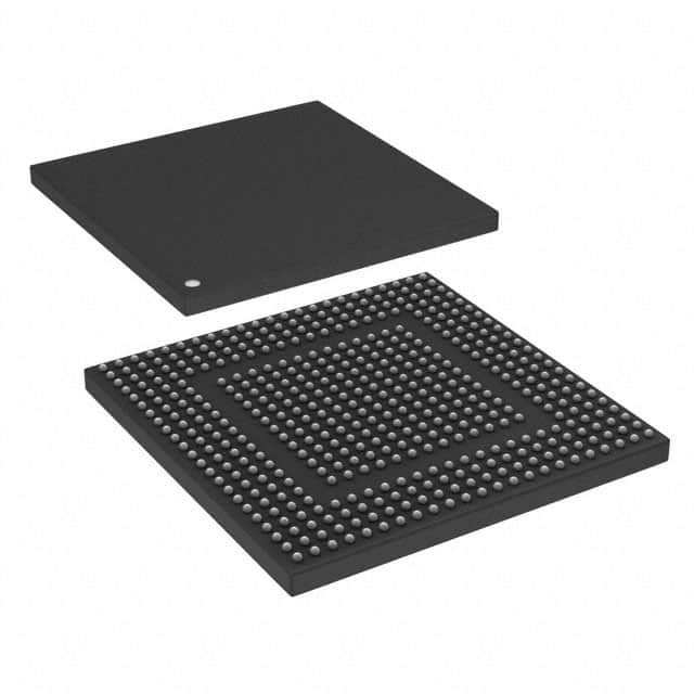
- Part No.:
- MCIMX31CVMN4DR2
- Manufacturer:
- NXP Semiconductors
- Category:
- Microprocessors
- Package:
- 473-LFBGA
- Datasheet:
-
 MCIMX31CVMN4DR2.pdf
- Description:
- IC MPU I.MX31 400MHZ 473LFBGA
- Quantity:
- Payment:

- Shipping:

Inventory:3,642
Please send an inquiry. Send us your inquiry, and we will respond immediately.
Product details
Overview
MCIMX31CVMN4DR2 from NXP Semiconductors (formerly Freescale) is an industrial- and automotive-grade multimedia applications processor built around the ARM1136JF-S core operating at 400 MHz. It integrates MPEG-4 hardware encoder (VGA @ 30 fps), Vector Floating Point (VFP11) co-processor, Autonomous Image Processing Unit (IPU), and SDMA controller. Designed for infotainment and human-machine interface systems in extended temperature environments (–40°C to +85°C), it supports DDR, NAND Flash, USB 2.0 OTG, SDHC, and ATA interfaces.
For engineers reviewing the MCIMX31CVMN4DR2 datasheet, MCIMX31CVMN4DR2 pinout, MCIMX31CVMN4DR2 application, or MCIMX31CVMN4DR2 equivalent, key selection considerations include its 473-ball MAPBGA package (19 × 19 mm, 0.8 mm pitch), dual-Vt 90 nm process, DVFS-capable power management, and absence of integrated GPU - distinguishing it from non-L variants and confirming its role as a cost-optimized, graphics-light multimedia SoC for deterministic embedded control.
Technical Context
The MCIMX31CVMN4DR2 implements the ARM v6 architecture with an 8-stage pipeline, Jazelle® Java acceleration, SIMD DSP extensions, and integrated MMUs with micro-TLBs backed by unified main TLBs. Its memory subsystem includes 16 KB instruction and 16 KB data L1 caches, 128 KB unified L2 cache, 32 KB ROM, and 16 KB SRAM - all accessible via high-speed AMBA L2 interface and optimized for low-latency interrupt handling and cache-coherent peripheral access.
Power management is implemented through multiple clock/power domains, independent gating, dynamic voltage and frequency scaling (DVFS), and state retention mode (QVCC = 0.95 V). The chip-level electrical specification mandates core supply (QVCC/QVCC1/QVCC4) between 1.22 V–1.47 V at 400 MHz, I/O supplies (NVCCx) from 1.75 V–3.1 V, and strict thermal limits: max junction temperature 105°C, RθJA = 29°C/W on 4-layer board.
Key Specifications
| Parameter | Value and Actual Design Meaning |
|---|---|
| Core Architecture | ARM1136JF-S, ARM v6, 8-stage pipeline with Jazelle and SIMD support - enables real-time Java bytecode execution and efficient media processing without host CPU overhead. |
| Clock Speed | 400 MHz maximum ARM core frequency - delivers deterministic performance for VGA-resolution video encoding and real-time audio streaming in resource-constrained systems. |
| MPEG-4 Encoder | Hardware-accelerated encode up to VGA @ 30 fps - offloads CPU, reduces system memory bandwidth, and enables low-power viewfinder operation without ARM involvement. |
| Memory Interfaces | DDR, SDRAM, NAND Flash, NOR Flash, SRAM, PSRAM - supports boot-from-NAND, multi-bank memory mapping, and flexible external storage for automotive HMI firmware and media assets. |
| Package | MAPBGA-473, 19 × 19 mm, 0.8 mm pitch, RoHS-compliant (Case 1931, MSL 3) - ensures mechanical stability in automotive vibration environments and compatibility with standard PCB assembly processes. |
| Operating Temperature | –40°C to +85°C ambient - qualified for under-dash automotive infotainment and industrial panel PCs requiring extended thermal reliability without derating. |
| Power Management | DVFS, power gating, clock gating, state retention (0.95 V core) - enables sub-100 µA deep-sleep current and rapid wake-up for always-on UI responsiveness in battery-backed systems. |
Pinout & Package
MCIMX31CVMN4DR2 is housed in a 473-ball MAPBGA package (Case 1931), 19 mm × 19 mm, 0.8 mm ball pitch, RoHS-compliant and moisture-sensitive level 3 (MSL 3). Ball assignment follows Freescale's documented pinout for MCIMX31C silicon revision 2.0.1, with dedicated power/ground banks, configurable I/O banks supporting 1.8 V/2.5 V/3.3 V signaling, and differential clock inputs (CKIL/CKIH).
| Pin/Terminal | Circuit Role | Design Meaning |
|---|---|---|
| CKIL / CKIH | Low-/High-frequency reference clock inputs | CKIL (32.768 kHz) clocks RTC/watchdog; CKIH (15–75 MHz) feeds DPLLs - critical for boot sequence, DVFS table validity, and timing-critical peripherals like USB OTG. |
| QVCC / QVCC1 / QVCC4 | Core voltage supply pins (ARM/L2/cache) | Must be regulated within 1.22–1.47 V; offset ≤15 mV between rails - violation causes USB HS data corruption and L2 cache instability. |
| NVCC1–NVCC10 | I/O voltage supply pins (grouped by function) | NVCC6/NVCC9 must be tied together; NVCC2/21/22 reserved for DDR only (1.75–1.95 V) - mismatch risks I/O latch-up or signal integrity failure. |
| GPIO1_5 / GPIO1_6 | Dedicated power-ready and tamper-detect inputs | GPIO1_5 is input-only (pull-up required if unused); GPIO1_6 enables irreversible tamper detection - used for secure boot enforcement in automotive telematics. |
| USBOTG_D+ / USBOTG_D− | USB 2.0 OTG differential data pair | Requires 90 Ω differential impedance and on-die termination - enables host/device mode switching without external transceiver for compact infotainment docking solutions. |
Key Features
| Feature | Design Value |
|---|---|
| MPEG-4 Hardware Encoder | Real-time VGA @ 30 fps encoding with on-the-fly post-processing - eliminates need for external codec IC and reduces BOM cost in rear-seat entertainment systems. |
| Autonomous Image Processing Unit (IPU) | Hardware-accelerated camera interface, blending, rotation, and display path control - enables zero-CPU-load viewfinder, overlay compositing, and dual-display output for instrument cluster + center stack. |
| Vector Floating Point (VFP11) Co-processor | Tightly coupled ARM v6 FPU supporting 3D graphics math and audio FFTs - accelerates navigation map rendering and voice recognition algorithms without floating-point emulation overhead. |
| Smart DMA (SDMA) Controller | 26-channel programmable DMA with peripheral-to-peripheral transfers - relieves ARM core from audio streaming, sensor data acquisition, and display buffer updates in real-time HMI applications. |
| Security Subsystem (RNGA, SCC, RTIC) | FIPS-140 compliant random number generator, secure RAM, and runtime integrity checkers - provides cryptographic key generation and boot authentication for OEM firmware protection in connected vehicles. |
Applications
| Automotive Infotainment Head Unit | Industrial Human-Machine Interface (HMI) |
|---|---|
Use Scenario: Central display unit integrating navigation, media playback, Bluetooth hands-free, and vehicle telemetry in passenger vehicles. IC Role / Device Role / Timing Role: Primary application processor executing Linux-based IVI stack, managing USB OTG for smartphone mirroring, SDHC for map updates, and IPU for dual-display rendering. Use Value: Hardware MPEG-4 encode enables real-time dashcam recording while running navigation; DVFS maintains thermal envelope under continuous 400 MHz load during route calculation. |
Use Scenario: Ruggedized touch-panel controller for factory automation, medical device UI, or building management system. IC Role / Device Role / Timing Role: Real-time HMI engine driving LCD/TFT display, sampling capacitive touch, communicating via UART/USB to PLCs, and logging sensor data to NAND Flash. Use Value: 16 KB SRAM buffers audio streams for alarm tones without DRAM access; -40°C to +85°C rating ensures reliable operation in unconditioned industrial enclosures. |
| Portable Medical Imaging Terminal | Secure Telematics Control Unit |
Use Scenario: Handheld ultrasound or point-of-care imaging device requiring low-latency image capture, processing, and local display. IC Role / Device Role / Timing Role: Image acquisition processor interfacing to CMOS sensor via parallel camera port, applying real-time IPU filters, and rendering processed frames to LCD. Use Value: Autonomous IPU performs noise reduction and edge enhancement in hardware - cuts ARM CPU utilization by >70% versus software-only pipeline, extending battery life. |
Use Scenario: Cellular-connected vehicle gateway performing OTA updates, remote diagnostics, and encrypted CAN message routing. IC Role / Device Role / Timing Role: Secure boot root-of-trust processor validating firmware signatures using RNGA and SCC, then managing USB/SDHC update paths and CAN bus arbitration. Use Value: Tamper-detect GPIO1_6 triggers secure erase on physical intrusion; RTIC validates peripheral register integrity before CAN frame transmission - meets ISO/SAE 21434 cybersecurity requirements. |
Equivalent & Alternatives
The following parts are listed as comparable options for similar multimedia applications processor applications.
| Alternative Part | Technical Difference | Application Difference | Selection Advice |
|---|---|---|---|
| i.MX353CJM8C | ARM Cortex-A8 @ 532 MHz, integrated 2D GPU, 256 MB DDR2 on-package, no MPEG-4 encoder | Higher CPU performance but lacks hardware video encode; targets richer GUIs over raw media encode | Select when prioritizing OpenGL ES graphics over real-time VGA encoding; requires redesign for DDR2 integration and Cortex toolchain migration. |
| MCIMX27CZK8C | ARM926EJ-S @ 400 MHz, no VFP, no L2 cache, MPEG-4 encode limited to QCIF @ 30 fps | Lower-cost, lower-power legacy option with reduced multimedia throughput and no vector math acceleration | Choose for cost-sensitive, non-GUI HMI where VGA encode and 3D graphics are unnecessary; retains same pin-compatible footprint but lower peripheral count. |
Compared with i.MX353CJM8C and MCIMX27CZK8C, MCIMX31CVMN4DR2 uniquely balances ARM11 performance, hardware MPEG-4 encode, VFP acceleration, and industrial temperature support - making it optimal for infotainment systems requiring real-time video processing without GPU overhead or Cortex migration complexity.
Availability
MCIMX31CVMN4DR2 is available at Aetrix Electronics and suitable for automotive infotainment head units, industrial HMI panels, and portable medical imaging terminals requiring stable component supply across extended product lifecycles.
Supply support for MCIMX31CVMN4DR2 includes scheduled delivery planning, volume procurement assistance, BOM continuity management, traceable sourcing, and lifecycle availability coordination for OEM customers, industrial embedded developers, connected-device designers, and electronics production programs.
Manufacturer
NXP Semiconductors is a global semiconductor leader focused on secure connectivity solutions for automotive, industrial, and IoT applications, with roots in Freescale's embedded processor heritage.
The i.MX31 family - including MCIMX31CVMN4DR2 - was engineered specifically for high-reliability, low-power multimedia processing in automotive and industrial environments, emphasizing deterministic real-time performance, extended temperature operation, and hardware-accelerated video/audio functions.
FAQ
What is the silicon revision and key functional difference of MCIMX31CVMN4DR2?
The MCIMX31CVMN4DR2 is silicon revision 2.0.1, which includes an updated iROM enabling boot from USB High-Speed and SD/MMC - a critical enhancement over revision 2.0 for field-upgradable automotive systems. This revision also resolves errata ENGcm02610 related to USB HS data corruption at low core voltages, ensuring robust high-speed peripheral operation across the full 1.22–1.47 V QVCC range.
Does MCIMX31CVMN4DR2 include a graphics processing unit (GPU)?
No, MCIMX31CVMN4DR2 does not include an integrated GPU. The MCIMX31C series includes GPU functionality only in non-L variants; the "C" suffix denotes the base multimedia processor without GPU, while "LC" explicitly indicates GPU removal. MCIMX31CVMN4DR2 relies on its Vector Floating Point (VFP11) co-processor and IPU for 2D/3D acceleration - sufficient for UI rendering and video overlays but not for complex 3D gaming or OpenGL ES workloads.
What are the mandatory power supply sequencing requirements for MCIMX31CVMN4DR2?
MCIMX31CVMN4DR2 requires strict power-up sequencing: QVCC (core) must stabilize before NVCC (I/O) rails, and all QVCC rails (QVCC/QVCC1/QVCC4) must remain within ±15 mV of each other during operation. Failure to meet this causes USB HS transfer errors and L2 cache corruption. Power-down sequencing is less restrictive but recommends disabling PLLs before core voltage ramp-down to prevent clock domain metastability.
Can MCIMX31CVMN4DR2 support dual-display output simultaneously?
Yes, MCIMX31CVMN4DR2 supports dual-display output via its integrated Image Processing Unit (IPU), which provides two independent display paths - one for LCD/TFT and another for TV encoder (NTSC/PAL). The IPU handles blending, rotation, and scaling in hardware, allowing concurrent rendering of instrument cluster graphics and infotainment UI without ARM CPU intervention or external compositor IC.
What security features are implemented in MCIMX31CVMN4DR2 for automotive use cases?
MCIMX31CVMN4DR2 integrates three hardware security blocks: RNGA (FIPS-140 compliant random number generator), SCC (Security Controller with Secure RAM for key storage), and RTIC (Run-Time Integrity Checker for peripheral register validation). These enable secure boot, cryptographic key generation, tamper detection (via GPIO1_6), and runtime firmware integrity verification - meeting foundational requirements for ISO/SAE 21434-compliant automotive telematics and gateway modules.
MCIMX31CVMN4DR2 Specifications
- Product attributes
- Attribute value
- Manufacturer:
- NXP Semiconductors
- Package/Case:
- 473-LFBGA
- Series:
- i.MX31
- Packaging:
- Tape & Reel (TR)
- Product Status:
- Obsolete
- Core Processor:
- ARM1136JF-S
- Number of Cores/Bus Width:
- 1 Core, 32-Bit
- Speed:
- 400MHz
- Co-Processors/DSP:
- Multimedia; GPU, IPU, MPEG-4, VFP
- RAM Controllers:
- DDR
- Graphics Acceleration:
- Yes
- Display & Interface Controllers:
- Keyboard, Keypad, LCD
- Ethernet:
- -
- SATA:
- -
- USB:
- USB 2.0 (3)
- Voltage - I/O:
- 1.8V, 2.0V, 2.5V, 2.7V, 3.0V
- Operating Temperature:
- -40°C ~ 85°C (TA)
- Grade:
- -
- Qualification:
- -
- Security Features:
- Random Number Generator, RTIC, Secure Fusebox, Secure JTAG, Secure Memory
- Mounting Type:
- Surface Mount
- Supplier Device Package:
- 473-LFBGA (19x19)
- Additional Interfaces:
- 1-Wire, AC97, ATA, FIR, I2C, I2S, MMC/SD/SDIO, MSHC, PCMCIA, SDHC, SIM, SPI, SSI, UART
MCIMX31CVMN4DR2 FAQ
1.How can I place an order for MCIMX31CVMN4DR2 through Aetrix?
Please submit a Request for Quotation (RFQ) for MCIMX31CVMN4DR2 on Aetrix. Our sales agent will provide a competitive quotation and guide you through the order confirmation once you accept the terms.
2.Are the price and stock information for MCIMX31CVMN4DR2 reliable?
The price and inventory of MCIMX31CVMN4DR2 are updated periodically and may fluctuate due to market conditions. Stock and pricing data are typically refreshed every 24 hours. Quotation validity for MCIMX31CVMN4DR2 is usually 5 days.
3.What payment methods are accepted for MCIMX31CVMN4DR2?
We accept Wire Transfer, PayPal, Credit Card, Western Union, MoneyGram, and Escrow for MCIMX31CVMN4DR2 transactions.
Note: Certain payment methods may incur a processing fee.
4.How is shipping managed for MCIMX31CVMN4DR2?
MCIMX31CVMN4DR2 orders can be shipped via leading logistics carriers, including DHL, UPS, FedEx, TNT, or Registered Mail.
Once your MCIMX31CVMN4DR2 order is processed, you will receive an email with the shipment details and tracking number.
Note: Tracking information may take up to 24 hours to appear. Express delivery typically takes 3–5 business days.
5.How can I obtain technical support or documentation for MCIMX31CVMN4DR2?
For technical support, including MCIMX31CVMN4DR2 datasheets, pinout diagrams, or application guidance, please contact our engineering support team. They can provide detailed documentation and assistance for your MCIMX31CVMN4DR2 requirements.
6.How does Aetrix verify that MCIMX31CVMN4DR2 is sourced from the original manufacturer or authorized distributors?
All MCIMX31CVMN4DR2 products on Aetrix are procured from qualified distributors and authorized channels. Our dedicated quality assurance team conducts strict verification, including traceability checks and, if necessary, third-party testing. This ensures that MCIMX31CVMN4DR2 meets industry standards.
7.What is the process for return or replacement of MCIMX31CVMN4DR2?
All MCIMX31CVMN4DR2 units undergo pre-shipment inspection (PSI). If there is an issue with MCIMX31CVMN4DR2, returns or replacements are accepted under the following conditions:
1.Quantity discrepancies, incorrect items, or visible external defects (such as breakage or corrosion), acknowledged by Aetrix.
2.The issue is reported within 90 days of delivery.
3.The MCIMX31CVMN4DR2 part is unused and in its original packaging.
Return procedure for MCIMX31CVMN4DR2:
1.Submit a request within 90 days.
2.Obtain a Return Material Authorization (RMA) from Aetrix.
MCIMX31CVMN4DR2 Tags

-
AT91SAM9260B-CU-999
Microchip Technology
-
AT91SAM9G25-CU
Microchip Technology

-
ATSAMA5D27C-CU
Microchip Technology
-
AT91SAM9X35-CU
Microchip Technology
-
AT91SAM9X25-CU
Microchip Technology

-
MCIMX6Y2CVM08AB
NXP Semiconductors
.JPG)
-
AM3352BZCZ100
Texas Instruments
-
AT91SAM9260B-CU
Microchip Technology

-
AT91SAM9260B-QU
Microchip Technology

-
ATSAMA5D31A-CU
Microchip Technology
-
AT91SAM9G20B-CU-999
Microchip Technology
-
MCIMX6Y2CVM05AB
NXP Semiconductors
Tech Hub

A practical engineering guide to 3.3V and 5V logic compatibility, input thresholds, resistor dividers, translator ICs, MOSFET level shifting, I2C pull-ups, timing limits and power-sequencing risks.

The 74HC595 uses push-pull logic outputs, while the TPIC6B595 uses 50 V open-drain DMOS sinks for higher-power loads. This guide compares timing, current limits, 3.3 V interfacing, load wiring, thermal…

The 74HC595 converts serial data into eight stable parallel outputs. This guide covers pin functions, shift and storage timing, OE and MR behavior, drive-current limits, cascading, voltage compatibilit…

A technical comparison of level-sensitive latches and edge-triggered flip-flops, covering timing windows, setup and hold limits, master–slave operation, time borrowing, race-through, HDL inference and…

A D latch stores one bit while Enable controls when data can pass. This reference covers gate-level operation, truth tables, transparency, setup and hold timing, LE versus OE, common ICs and practical …

An SR latch stores one bit through cross-coupled feedback. This engineering reference covers NOR and NAND implementations, truth tables, forbidden-state recovery, gated operation, switch debouncing, fa…

Latch circuits retain one bit through feedback. This technical reference covers SR and D latches, truth tables, transparency, timing limits, latch-versus-flip-flop behavior, applications and common log…

An engineering guide to LED driver operation, constant-current and constant-voltage outputs, linear and switching topologies, dimming, IC selection, calculations, replacement compatibility, and fault c…

Operational amplifier guide covering op amp basics, feedback, ideal vs real op amps, common configurations, buffer circuits, offset, bias current, gain-bandwidth, slew rate, rail-to-rail limits and sel…

Jumper cables guide covering safe connection order, red and black clamp placement, final ground connection, cable gauge, length, clamp quality, copper vs CCA cables, jump starter comparison and battery…


