
 My Inquiry
 My Account


NXP Semiconductors MCIMX6D5EYM12AE
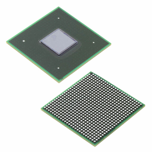
- Part No.:
- MCIMX6D5EYM12AE
- Manufacturer:
- NXP Semiconductors
- Category:
- Microprocessors
- Package:
- 624-LFBGA, FCBGA
- Datasheet:
-
 MCIMX6D5EYM12AE.pdf
- Description:
- IC MPU I.MX6D 1.2GHZ 624FCPBGA
- Quantity:
- Payment:

- Shipping:

Inventory:4,641
Please send an inquiry. Send us your inquiry, and we will respond immediately.
Product details
Overview
MCIMX6D5EYM12AE from NXP Semiconductors is an industrial-grade i.MX 6Dual applications processor featuring dual Arm Cortex-A9 cores running at 1.2 GHz, integrated VPU and GPU, 1 MB L2 cache, and support for DDR3/DDR3L/LPDDR2-800 memory. It delivers 1080p video decode/encode, OpenGL ES 2.0 3D graphics (200 MTri/s), and hardware-accelerated 2D/Vector graphics for embedded HMI and industrial control systems.
For engineers reviewing the MCIMX6D5EYM12AE datasheet, MCIMX6D5EYM12AE pinout, MCIMX6D5EYM12AE application, or MCIMX6D5EYM12AE equivalent, key selection criteria include industrial temperature range (−40°C to +105°C), FCPBGA-624 package with 0.8 mm pitch, dual-core performance with TrustZone security, and verified multimedia subsystem compatibility (VPU, IPUv3H, GPU3Dv4, GPU2Dv2, GPUVGv2).
Technical Context
The MCIMX6D5EYM12AE implements a symmetric dual-core Arm Cortex-A9 MPCore platform with 32 KB L1 instruction and data caches per core, 1 MB shared L2 cache, SCU, GIC supporting 128 interrupts, and NEON MPE co-processor. It integrates dedicated hardware accelerators including VPU (H.264 BP/MP/HP up to 1080p30), dual IPUv3H for image processing, and ASRC for multi-channel audio sample rate conversion.
Power management includes DVFS, software state retention, power gating, and on-die temperature sensing. Clock architecture features eight PLLs, on-chip oscillators (24 MHz crystal input required for USB), and CCM-based dynamic clock gating across all domains - enabling operation in industrial environments with sustained thermal profiles.
Key Specifications
| Parameter | Value and Actual Design Meaning |
|---|---|
| CPU Core | Dual Arm Cortex-A9 @ 1.2 GHz - enables real-time deterministic execution of dual-threaded industrial firmware with TrustZone isolation. |
| L2 Cache | 1 MB unified - reduces external memory bandwidth pressure and improves deterministic latency for control-critical tasks. |
| Memory Interface | 64-bit DDR3/DDR3L/LPDDR2-800 - supports up to 1066 MT/s DDR3, enabling high-throughput frame buffering for dual-display or camera+display pipelines. |
| Video Processing | VPU with H.264 BP/MP/HP decode/encode up to 1080p30 - offloads CPU for surveillance, digital signage, and video analytics preprocessing. |
| Graphics Acceleration | GPU3Dv4 (OpenGL ES 2.0, 200 MTri/s), GPU2Dv2, GPUVGv2 - renders complex vector-based HMIs at 60 fps on HD displays without CPU burden. |
| Security | CAAM (16 KB secure RAM), SNVS, CSU, A-HABv4 with SHA-256 & 2048-bit RSA - enables secure boot, encrypted firmware updates, and DRM-compliant content playback. |
| Temperature Grade | Industrial (−40°C to +105°C junction) - qualified for uncooled deployment in factory automation, transportation, and energy infrastructure. |
Pinout & Package
MCIMX6D5EYM12AE is housed in a 21 mm × 21 mm FCPBGA package with 624 balls and 0.8 mm pitch. The package is lidded and RoHS-compliant, designed for industrial PCB assembly with controlled thermal dissipation and mechanical robustness.
| Pin/Terminal | Circuit Role | Design Meaning |
|---|---|---|
| CLK_24M_IN | Primary Oscillator Input | Mandatory 24 MHz crystal reference for USB PHY, system clocks, and PLL synchronization - absence prevents USB and critical timing domains from initializing. |
| VDD_ARM | Core Voltage Supply | 1.2 V ±3% supply for Arm Cortex-A9 cores and L1/L2 caches - requires low-noise regulation and local decoupling to sustain 1.2 GHz operation. |
| VDD_SOC | System-on-Chip Voltage | 1.2 V ±3% supply powering MMDC, GPU, VPU, and interconnect fabric - shared rail with strict sequencing relative to VDD_ARM. |
| BOOT_MODE[1:0] | Boot Configuration | Two-pin strap controlling boot source (eMMC, NAND, SPI NOR, SD) - determines initial firmware load path and security policy enforcement level. |
| ENET_RXD[3:0]/TXD[3:0] | Gigabit Ethernet Interface | 8-pin RMII/RGMII-capable interface supporting IEEE 1588 PTP - enables time-synchronized industrial networking with ≤400 Mbps real-world throughput. |
| CSI_DATA[7:0]/CLK | Parallel Camera Interface | 10-pin high-speed CMOS sensor interface (up to 240 MHz pixel clock) - supports direct connection to industrial area-scan cameras without bridge ICs. |
Key Features
| Feature | Design Value |
|---|---|
| Smart Speed Technology | Dynamic voltage/frequency scaling across CPU, GPU, VPU, and memory domains - reduces active power by >40% during partial-load HMI rendering or video playback. |
| Dual IPUv3H Image Processors | Hardware-accelerated deinterlacing, color space conversion (YUV↔RGB), scaling, and overlay composition - enables simultaneous display of camera feed + GUI layer with zero CPU overhead. |
| Multi-Mode DDR Controller (MMDC) | Supports interleaved DDR3/DDR3L/LPDDR2 with on-the-fly calibration - ensures reliable memory operation across industrial temperature extremes and voltage droop events. |
| FlexCAN v2.0B Dual Channels | Two independent 1 Mbps CAN interfaces with message RAM and loopback mode - meets automotive-grade diagnostics and distributed control requirements in machinery and EV charging systems. |
| Secure Boot with A-HABv4 | SHA-256 hash verification, 2048-bit RSA signature validation, and version-controlled firmware images - prevents unauthorized code execution and enforces field-upgrade integrity. |
Applications
| Industrial HMI Terminal | Digital Signage Player |
|---|---|
Use Scenario: Ruggedized touch panel in factory floor control station with dual 1080p displays and real-time alarm visualization. IC Role / Device Role / Timing Role: Primary applications processor executing Linux-based HMI stack, driving parallel LCD + HDMI outputs, and managing CAN-connected PLCs. Use Value: Dual Cortex-A9 cores handle UI rendering and control logic concurrently; GPU3Dv4 ensures smooth 60 fps animation; VPU enables local video diagnostics feed without cloud dependency. |
Use Scenario: Fanless media player in retail kiosk delivering 4K-downscaled content, interactive promotions, and remote CMS updates over cellular. IC Role / Device Role / Timing Role: System-on-chip handling video decode, OpenGL ES 2.0 UI compositing, eMMC storage management, and LTE modem interfacing via USB OTG. Use Value: Hardware VPU decodes H.264/H.265 streams at <1W; GPU2Dv2 accelerates bitmap overlays; CAAM secures OTA firmware packages against tampering. |
| Railway Onboard Display | Medical Imaging Edge Node |
Use Scenario: EN50155-certified passenger information display showing live GPS maps, door status, and emergency alerts in rolling stock. IC Role / Device Role / Timing Role: Real-time multimedia processor synchronizing GPS time (via UART/PPS), LVDS display output, and redundant FlexCAN communication to train control network. Use Value: IEEE 1588-capable ENET enables sub-millisecond timestamp alignment; industrial temp grade ensures reliability in unheated carriages; SNVS RTC maintains accurate scheduling during power loss. |
Use Scenario: Portable ultrasound device requiring real-time B-mode image reconstruction, DICOM export, and touchscreen-guided workflow. IC Role / Device Role / Timing Role: High-performance imaging SoC acquiring raw sensor data via CSI-2, applying GPU-accelerated beamforming, and rendering grayscale video to MIPI DSI display. Use Value: Dual IPUv3H performs real-time YUV→RGB conversion and contrast enhancement; ASRC handles multi-channel audio feedback; secure boot validates FDA-compliant firmware signatures. |
Equivalent & Alternatives
The following parts are listed as comparable options for similar dual-core applications processor applications.
| Alternative Part | Technical Difference | Application Difference | Selection Advice |
|---|---|---|---|
| MCIMX6D6AVT10AC | 1.0 GHz max frequency, commercial temp (−20°C to +105°C), same FCPBGA-624 package | Lower peak compute; suitable for cost-sensitive non-critical HMIs where 1.2 GHz headroom is unnecessary | Select when thermal budget or BOM cost constraints outweigh need for maximum dual-core throughput. |
| i.MX 8M Nano QuadLite (MIMX8MN5CVTIZAB) | Quad Cortex-A53 @ 1.6 GHz, integrated GC7000UL GPU, LPDDR4 support, newer Armv8-A ISA | Higher single-thread performance, advanced security (TEE, HABv4.4), but higher power and no pin compatibility | Choose for next-generation designs requiring AI inference acceleration, Android compatibility, or future-proof longevity beyond i.MX 6 lifecycle. |
Compared with MCIMX6D5EYM12AE, MCIMX6D6AVT10AC trades 200 MHz clock headroom for broader commercial qualification, while i.MX 8M Nano offers architectural modernization at the cost of redesign effort - making MCIMX6D5EYM12AE optimal for stable, thermally constrained industrial deployments needing proven reliability.
Availability
MCIMX6D5EYM12AE is available at Aetrix Electronics and suitable for industrial HMI terminals, digital signage players, railway onboard displays, and medical edge nodes requiring stable component supply across extended product lifecycles.
Supply support for MCIMX6D5EYM12AE includes scheduled delivery planning, volume procurement assistance, BOM continuity management, traceable sourcing, and lifecycle availability coordination for OEM customers, industrial embedded developers, connected-device designers, and electronics production programs.
Manufacturer
NXP Semiconductors is a global semiconductor leader focused on secure connectivity solutions for automotive, industrial, and IoT markets, with deep expertise in Arm-based applications processors and edge AI acceleration.
The i.MX 6Dual series - including MCIMX6D5EYM12AE - was engineered specifically for industrial applications demanding long-term availability, extended temperature operation, and hardware-enforced security in resource-constrained environments.
FAQ
What is the maximum operating frequency of the MCIMX6D5EYM12AE and under what conditions?
The MCIMX6D5EYM12AE operates at a guaranteed maximum frequency of 1.2 GHz across its full industrial temperature range (−40°C to +105°C junction). This rating assumes use of the mandatory 24 MHz input clock for USB and system PLLs, proper power delivery (VDD_ARM and VDD_SOC within ±3% tolerance), and adherence to thermal design guidelines specified in the IMX6DQIEC datasheet. Frequency scaling below 1.2 GHz is supported via DVFS for power optimization.
Does the MCIMX6D5EYM12AE support secure boot, and which cryptographic algorithms are implemented?
Yes, the MCIMX6D5EYM12AE supports Advanced High Assurance Boot (A-HABv4) with SHA-256 hash verification, 2048-bit RSA signature validation, and version-controlled firmware images. These functions are enforced by the CSU and CAAM modules, with keys stored in eFUSEs and secure RAM. The implementation complies with NIST SP 800-140 and enables chain-of-trust boot for industrial firmware integrity.
Which display interfaces does the MCIMX6D5EYM12AE natively support, and what are their maximum resolutions?
The MCIMX6D5EYM12AE supports five native display interfaces: parallel RGB (24-bit, up to WUXGA 1920×1200@60 Hz), LVDS (dual-port, up to WUXGA@60 Hz), HDMI 1.4 (up to 1080p60), MIPI DSI (2-lane, up to 1080p60), and internal LCD controller. Total raw pixel throughput across all active interfaces is capped at 450 Mpixels/sec (24 bpp), allowing concurrent dual-HD or quad-WXGA configurations depending on interface selection and bandwidth allocation.
Can the MCIMX6D5EYM12AE directly interface with MIPI CSI-2 camera sensors, and what lane configurations are supported?
Yes, the MCIMX6D5EYM12AE includes a dedicated MIPI CSI-2 receiver supporting 1–4 data lanes plus one clock lane. It achieves up to 1000 Mbps/lane in 1–3 lane mode and 800 Mbps/lane in 4-lane mode, enabling direct connection to industrial CMOS sensors such as ON Semiconductor AR0237 or Sony IMX290. The CSI-2 interface is fully integrated with the IPUv3H for zero-copy image processing and DMA-managed frame buffering.
What is the package type and ball count of the MCIMX6D5EYM12AE, and are there any special PCB layout considerations?
The MCIMX6D5EYM12AE uses a 21 mm × 21 mm FCPBGA package with 624 balls and 0.8 mm pitch. It is lidded and RoHS-compliant. Critical layout considerations include strict power plane segmentation (separate VDD_ARM/VDD_SOC planes), controlled-impedance routing for DDR3/LVDS/HDMI traces, thermal via arrays under the die pad, and adherence to NXP's recommended land pattern (document AN4948) to ensure solder joint reliability in thermal cycling environments.
MCIMX6D5EYM12AE Specifications
- Product attributes
- Attribute value
- Manufacturer:
- NXP Semiconductors
- Package/Case:
- 624-LFBGA, FCBGA
- Series:
- i.MX6D
- Packaging:
- Tray
- Product Status:
- Active
- Core Processor:
- ARM® Cortex®-A9
- Number of Cores/Bus Width:
- 2 Core, 32-Bit
- Speed:
- 1.2GHz
- Co-Processors/DSP:
- Multimedia; NEON™ SIMD
- RAM Controllers:
- LPDDR2, LVDDR3, DDR3
- Graphics Acceleration:
- Yes
- Display & Interface Controllers:
- Keypad, LCD
- Ethernet:
- 10/100/1000Mbps (1)
- SATA:
- SATA 3Gbps (1)
- USB:
- USB 2.0 + PHY (4)
- Voltage - I/O:
- 1.8V, 2.5V, 2.8V, 3.3V
- Operating Temperature:
- -20°C ~ 105°C (TJ)
- Grade:
- -
- Qualification:
- -
- Security Features:
- ARM TZ, Boot Security, Cryptography, RTIC, Secure Fusebox, Secure JTAG, Secure Memory, Secure RTC, Tamper Detection
- Mounting Type:
- Surface Mount
- Supplier Device Package:
- 624-FCPBGA (21x21)
- Additional Interfaces:
- CAN, I2C, I2S, MMC/SD/SDIO, SAI, SPI, SSI, UART
MCIMX6D5EYM12AE FAQ
1.How can I place an order for MCIMX6D5EYM12AE through Aetrix?
Please submit a Request for Quotation (RFQ) for MCIMX6D5EYM12AE on Aetrix. Our sales agent will provide a competitive quotation and guide you through the order confirmation once you accept the terms.
2.Are the price and stock information for MCIMX6D5EYM12AE reliable?
The price and inventory of MCIMX6D5EYM12AE are updated periodically and may fluctuate due to market conditions. Stock and pricing data are typically refreshed every 24 hours. Quotation validity for MCIMX6D5EYM12AE is usually 5 days.
3.What payment methods are accepted for MCIMX6D5EYM12AE?
We accept Wire Transfer, PayPal, Credit Card, Western Union, MoneyGram, and Escrow for MCIMX6D5EYM12AE transactions.
Note: Certain payment methods may incur a processing fee.
4.How is shipping managed for MCIMX6D5EYM12AE?
MCIMX6D5EYM12AE orders can be shipped via leading logistics carriers, including DHL, UPS, FedEx, TNT, or Registered Mail.
Once your MCIMX6D5EYM12AE order is processed, you will receive an email with the shipment details and tracking number.
Note: Tracking information may take up to 24 hours to appear. Express delivery typically takes 3–5 business days.
5.How can I obtain technical support or documentation for MCIMX6D5EYM12AE?
For technical support, including MCIMX6D5EYM12AE datasheets, pinout diagrams, or application guidance, please contact our engineering support team. They can provide detailed documentation and assistance for your MCIMX6D5EYM12AE requirements.
6.How does Aetrix verify that MCIMX6D5EYM12AE is sourced from the original manufacturer or authorized distributors?
All MCIMX6D5EYM12AE products on Aetrix are procured from qualified distributors and authorized channels. Our dedicated quality assurance team conducts strict verification, including traceability checks and, if necessary, third-party testing. This ensures that MCIMX6D5EYM12AE meets industry standards.
7.What is the process for return or replacement of MCIMX6D5EYM12AE?
All MCIMX6D5EYM12AE units undergo pre-shipment inspection (PSI). If there is an issue with MCIMX6D5EYM12AE, returns or replacements are accepted under the following conditions:
1.Quantity discrepancies, incorrect items, or visible external defects (such as breakage or corrosion), acknowledged by Aetrix.
2.The issue is reported within 90 days of delivery.
3.The MCIMX6D5EYM12AE part is unused and in its original packaging.
Return procedure for MCIMX6D5EYM12AE:
1.Submit a request within 90 days.
2.Obtain a Return Material Authorization (RMA) from Aetrix.
MCIMX6D5EYM12AE Tags

-
AT91SAM9260B-CU-999
Microchip Technology
-
AT91SAM9G25-CU
Microchip Technology

-
ATSAMA5D27C-CU
Microchip Technology
-
AT91SAM9X35-CU
Microchip Technology
-
AT91SAM9X25-CU
Microchip Technology

-
MCIMX6Y2CVM08AB
NXP Semiconductors
.JPG)
-
AM3352BZCZ100
Texas Instruments
-
AT91SAM9260B-CU
Microchip Technology

-
AT91SAM9260B-QU
Microchip Technology

-
ATSAMA5D31A-CU
Microchip Technology
-
AT91SAM9G20B-CU-999
Microchip Technology
-
MCIMX6Y2CVM05AB
NXP Semiconductors
Tech Hub

A practical engineering guide to 3.3V and 5V logic compatibility, input thresholds, resistor dividers, translator ICs, MOSFET level shifting, I2C pull-ups, timing limits and power-sequencing risks.

The 74HC595 uses push-pull logic outputs, while the TPIC6B595 uses 50 V open-drain DMOS sinks for higher-power loads. This guide compares timing, current limits, 3.3 V interfacing, load wiring, thermal…

The 74HC595 converts serial data into eight stable parallel outputs. This guide covers pin functions, shift and storage timing, OE and MR behavior, drive-current limits, cascading, voltage compatibilit…

A technical comparison of level-sensitive latches and edge-triggered flip-flops, covering timing windows, setup and hold limits, master–slave operation, time borrowing, race-through, HDL inference and…

A D latch stores one bit while Enable controls when data can pass. This reference covers gate-level operation, truth tables, transparency, setup and hold timing, LE versus OE, common ICs and practical …

An SR latch stores one bit through cross-coupled feedback. This engineering reference covers NOR and NAND implementations, truth tables, forbidden-state recovery, gated operation, switch debouncing, fa…

Latch circuits retain one bit through feedback. This technical reference covers SR and D latches, truth tables, transparency, timing limits, latch-versus-flip-flop behavior, applications and common log…

An engineering guide to LED driver operation, constant-current and constant-voltage outputs, linear and switching topologies, dimming, IC selection, calculations, replacement compatibility, and fault c…

Operational amplifier guide covering op amp basics, feedback, ideal vs real op amps, common configurations, buffer circuits, offset, bias current, gain-bandwidth, slew rate, rail-to-rail limits and sel…

Jumper cables guide covering safe connection order, red and black clamp placement, final ground connection, cable gauge, length, clamp quality, copper vs CCA cables, jump starter comparison and battery…


