
 My Inquiry
 My Account


Microchip Technology MCP1257-E/MF
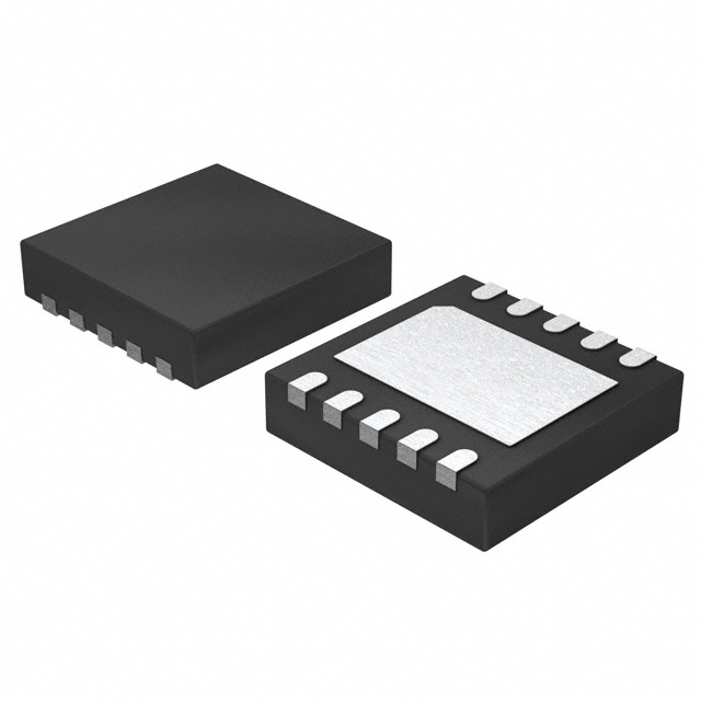
- Part No.:
- MCP1257-E/MF
- Manufacturer:
- Microchip Technology
- Package:
- 10-VFDFN Exposed Pad
- Datasheet:
-
 MCP1257-E/MF.pdf
- Description:
- IC REG CHG PUMP 3.3V 100MA 10DFN
- Quantity:
- Payment:

- Shipping:

Inventory:240
Please send an inquiry. Send us your inquiry, and we will respond immediately.
Product details
Overview
MCP1257-E/MF from Microchip Technology is a 10-pin DFN-packaged, inductorless 1.5x/2x charge pump DC/DC converter generating a regulated 3.3V output from 1.8V–3.6V input. It delivers up to 100 mA output current, maintains ±3.0% output voltage accuracy, features low 20 mVPP ripple at full load, and incorporates thermal shutdown and short-circuit protection - designed for battery-powered PIC® MCU bias and portable instrumentation.
For engineers reviewing the MCP1257-E/MF datasheet, MCP1257-E/MF pinout, MCP1257-E/MF application, or MCP1257-E/MF equivalent, this page provides verified functional identity (MCP1257 variant), confirmed SLEEP mode operation, exact 10-lead 3 mm × 3 mm DFN package mapping, validated pin roles including LBO and SLEEP terminals, and two manufacturer-confirmed alternative parts with documented functional and application differences.
Technical Context
The MCP1257-E/MF implements a switched-capacitor charge pump architecture with automatic 1.5x/2x mode selection based on input voltage and load conditions. Its regulation loop uses a feedback amplifier and bandgap reference to maintain 3.3V output across 1.8V–3.6V input range, while internal 650 kHz oscillator ensures fixed-frequency operation that avoids IF band interference.
SLEEP mode is activated via active-low logic on the SLEEP pin and employs pulse-skipping control to sustain regulation at reduced quiescent current (10–20 µA typical), increasing battery runtime without compromising bias stability for connected microcontrollers or real-time clocks.
Key Specifications
| Parameter | Value and Actual Design Meaning |
|---|---|
| Output Voltage | Fixed 3.3V - provides stable bias for 3.3V logic and PIC® MCUs without external feedback components. |
| Input Voltage Range | 1.8V to 3.6V - supports 2-cell alkaline/Ni-MH batteries and single lithium coin cells. |
| Max Output Current | 100 mA at VIN ≥ 2.2V - sufficient to power multiple low-power peripherals simultaneously. |
| Output Ripple | 20 mVPP at 100 mA - meets noise-sensitive analog and mixed-signal circuit requirements. |
| Switching Frequency | 650 kHz (typical) - enables compact ceramic capacitor filtering and avoids AM radio/IF interference bands. |
| SLEEP Mode IQ | 10–20 µA - extends battery life in standby while maintaining regulated VOUT for wake-up circuits. |
| Thermal Shutdown | 160°C threshold with 15°C hysteresis - protects against sustained overload or poor PCB thermal design. |
| Operating Temp | -40°C to +125°C junction - qualified for automotive under-hood and industrial embedded environments. |
Pinout & Package
Package: 10-lead, 3 mm × 3 mm DFN (exposed pad), RoHS-compliant, moisture sensitivity level 3.
| Pin/Terminal | Circuit Role | Design Meaning |
|---|---|---|
| 1 (LBO) | Open-drain low-battery indicator | Asserts logic low when VIN drops below 1.95V (typical); enables system-level battery monitoring without additional ICs. |
| 2 (SLEEP) | Active-low SLEEP mode enable | Pulls low to enter ultra-low-quiescent-current regulation mode; retains 3.3V bias during MCU sleep states. |
| 3 (C2-) | Flying capacitor negative terminal | Connects to 1 µF ceramic flying cap C2; critical for charge transfer efficiency in 1.5x/2x pumping cycles. |
| 4 (C1+) | Flying capacitor positive terminal | Connects to 1 µF ceramic flying cap C1; forms dual-capacitor charge pump network with C2. |
| 5 (VOUT) | Regulated 3.3V output | Delivers up to 100 mA; requires ≥2.2 µF ceramic bypass to GND for ripple suppression. |
| 6 (C2+) | Flying capacitor positive terminal | Completes second flying capacitor path; paired with Pin 3 (C2-) to store and transfer charge. |
| 7 (VIN) | Main power input | Accepts 1.8V–3.6V; requires ≥1 µF ceramic bypass to GND near pin for stable switching operation. |
| 8 (C1-) | Flying capacitor negative terminal | Paired with Pin 4 (C1+) to form first flying capacitor leg; must use low-ESR ceramic caps. |
| 9 (GND) | Power and signal reference | Common return for all capacitors and load; must be low-inductance connection to exposed pad. |
| 10 (SHDN) | Active-low shutdown control | Reduces total supply current to 0.25 µA (typical); compatible with 1.8V logic interfaces. |
Key Features
| Feature | Design Value |
|---|---|
| Inductorless charge pump | Eliminates EMI-prone magnetics and reduces BOM count to four ceramic capacitors only. |
| Auto-switching 1.5x/2x mode | Optimizes conversion efficiency across input range - e.g., 84.5% at VIN=1.8V/IOUT=10mA. |
| SLEEP mode with regulation | Maintains 3.3V output while drawing only 10–20 µA, enabling long-duration low-power MCU sleep. |
| Low-battery detection (LBO) | Provides early warning at 1.95V VIN threshold with 240 mV hysteresis to prevent false triggers. |
| Soft-start & foldback protection | Limits inrush current at startup and caps short-circuit current at 150 mA (typical) to protect IC and source. |
| Wide temperature operation | Full functionality from -40°C to +125°C junction enables deployment in harsh industrial and automotive settings. |
Applications
| PIC® MCU Bias Supply | Portable Measurement Instrument |
|---|---|
Use Scenario: Powering Microchip PIC® microcontrollers in handheld multimeters or data loggers operating from two AA batteries. IC Role / Device Role / Timing Role: Provides regulated 3.3V bias with SLEEP mode support for deep-sleep MCU operation between measurements. Use Value: Extends battery life by >3× vs. linear regulators due to 84.5% efficiency at light loads and sub-20 µA SLEEP current. | Use Scenario: Supplying precision analog front-end (AFE) and display driver in portable environmental sensors. IC Role / Device Role / Timing Role: Delivers low-noise 3.3V rail with <20 mVPP ripple to minimize ADC quantization error and LCD flicker. Use Value: Enables accurate 16-bit measurement resolution without adding ferrite beads or LC filters. |
| Home Automation Sensor Node | Real-Time Clock (RTC) Backup |
Use Scenario: Powering Zigbee/Thread wireless sensor nodes in smart thermostats or occupancy detectors. IC Role / Device Role / Timing Role: Supplies regulated 3.3V to RF transceiver and MCU during active transmission, then enters SLEEP mode during idle intervals. Use Value: Achieves multi-year battery life using standard CR2032 coin cell due to 0.25 µA shutdown and 10 µA SLEEP currents. | Use Scenario: Maintaining bias for RTC and SRAM during main power loss in industrial controllers. IC Role / Device Role / Timing Role: Acts as low-quiescent backup regulator, enabled by LBO signal to trigger graceful shutdown before brownout. Use Value: Prevents time/date corruption and memory loss by initiating save routines at precisely 1.95V VIN threshold. |
Equivalent & Alternatives
The following parts are listed as comparable options for similar charge pump DC/DC converter applications.
| Alternative Part | Technical Difference | Application Difference | Selection Advice |
|---|---|---|---|
| MCP1256-E/MF | Includes PGOOD output instead of LBO; identical SLEEP mode, package, and electrical specs otherwise. | Used where power-good status is required for system sequencing rather than battery monitoring. | Select when host MCU needs confirmation of valid 3.3V rail before initialization. |
| MCP1257T-E/MF | Tape-and-reel variant of same die; identical pinout, specs, and function; differs only in packaging format and reel quantity. | No functional difference - used exclusively for automated SMT assembly requiring reel feed. | Select for high-volume production; not suitable for manual prototyping or low-quantity orders. |
Compared with MCP1256-E/MF, the MCP1257-E/MF provides low-battery indication instead of power-good signaling - making it optimal for battery-run-time optimization and predictive shutdown. Compared with MCP1257T-E/MF, the base part offers tube packaging for sampling and small-batch development, avoiding reel-handling overhead.
Availability
MCP1257-E/MF is available at Aetrix Electronics and suitable for portable instrumentation, home automation sensor nodes, and PIC® MCU bias applications requiring stable component supply, extended temperature qualification, and long-term lifecycle support.
Supply support for MCP1257-E/MF includes scheduled delivery planning, volume procurement assistance, BOM continuity management, traceable sourcing, and lifecycle availability coordination for OEM customers, industrial embedded developers, connected-device designers, and electronics production programs.
Manufacturer
Microchip Technology Inc. is a leading provider of microcontroller, analog, and Flash-IP solutions, serving industrial, automotive, consumer, and communications markets with high-reliability silicon and development tools.
The MCP1257-E/MF belongs to Microchip's charge pump DC/DC converter product line, engineered specifically for compact, low-EMI, battery-powered systems needing regulated 3.3V rails without inductors - targeting portable medical devices, wireless sensors, and energy-harvesting edge nodes.
FAQ
What is the primary function of the MCP1257-E/MF?
The MCP1257-E/MF is an inductorless, regulated charge pump DC/DC converter that generates a precise 3.3V output from a 1.8V–3.6V input. Its core function is to provide efficient, low-noise bias for microcontrollers and analog circuitry in space-constrained, battery-operated systems - with special emphasis on SLEEP mode operation and low-battery detection via the LBO pin.
How does the SLEEP mode of the MCP1257-E/MF operate?
The MCP1257-E/MF enters SLEEP mode when the SLEEP pin is driven low, reducing quiescent current to 10–20 µA while maintaining regulated 3.3V output. This mode uses pulse-skipping control to conserve energy, resulting in higher output ripple (up to 60 mVPP) but preserving bias for wake-up peripherals - a key feature distinguishing MCP1257-E/MF from non-SLEEP variants like MCP1258.
What is the purpose of the LBO pin on the MCP1257-E/MF?
The LBO (Low-Battery Output) pin on the MCP1257-E/MF is an open-drain indicator that asserts logic low when input voltage falls below 1.95V (typical), with 240 mV hysteresis. It enables host systems to initiate controlled shutdown or data save operations before brownout - a defining feature of the MCP1257-E/MF versus PGOOD-equipped MCP1256-E/MF.
Which package type does the MCP1257-E/MF use?
The MCP1257-E/MF uses a 10-lead, 3 mm × 3 mm DFN package with exposed thermal pad. This RoHS-compliant, surface-mount package offers low thermal resistance (θJA = 57°C/W) and is optimized for high-density PCB layouts in portable electronics - distinct from the MSOP variant offered in same-family parts like MCP1257-E/MS.
Can the MCP1257-E/MF replace the MCP1256-E/MF directly?
No - the MCP1257-E/MF cannot serve as a direct replacement for the MCP1256-E/MF because it substitutes LBO functionality for PGOOD. While pinout and electrical specs are identical, the absence of PGOOD and presence of LBO changes system-level monitoring behavior. Interchange requires validation of host firmware logic for battery vs. power-good signaling.
MCP1257-E/MF Specifications
- Product attributes
- Attribute value
- Manufacturer:
- Microchip Technology
- Series:
- -
- Package/Case:
- 10-VFDFN Exposed Pad
- Packaging:
- Tube
- Product Status:
- Active
- Function:
- Step-Up
- Output Configuration:
- Positive
- Topology:
- Charge Pump
- Output Type:
- Fixed
- Number of Outputs:
- 1
- Voltage - Input (Min):
- 1.8V
- Voltage - Input (Max):
- 3.6V
- Voltage - Output (Min/Fixed):
- 3.3V
- Voltage - Output (Max):
- -
- Current - Output:
- 100mA
- Frequency - Switching:
- 650kHz
- Synchronous Rectifier:
- No
- Operating Temperature:
- -40°C ~ 125°C (TJ)
- Grade:
- -
- Qualification:
- -
- Mounting Type:
- Surface Mount
- Supplier Device Package:
- 10-DFN (3x3)
MCP1257-E/MF FAQ
1.How can I place an order for MCP1257-E/MF through Aetrix?
Please submit a Request for Quotation (RFQ) for MCP1257-E/MF on Aetrix. Our sales agent will provide a competitive quotation and guide you through the order confirmation once you accept the terms.
2.Are the price and stock information for MCP1257-E/MF reliable?
The price and inventory of MCP1257-E/MF are updated periodically and may fluctuate due to market conditions. Stock and pricing data are typically refreshed every 24 hours. Quotation validity for MCP1257-E/MF is usually 5 days.
3.What payment methods are accepted for MCP1257-E/MF?
We accept Wire Transfer, PayPal, Credit Card, Western Union, MoneyGram, and Escrow for MCP1257-E/MF transactions.
Note: Certain payment methods may incur a processing fee.
4.How is shipping managed for MCP1257-E/MF?
MCP1257-E/MF orders can be shipped via leading logistics carriers, including DHL, UPS, FedEx, TNT, or Registered Mail.
Once your MCP1257-E/MF order is processed, you will receive an email with the shipment details and tracking number.
Note: Tracking information may take up to 24 hours to appear. Express delivery typically takes 3–5 business days.
5.How can I obtain technical support or documentation for MCP1257-E/MF?
For technical support, including MCP1257-E/MF datasheets, pinout diagrams, or application guidance, please contact our engineering support team. They can provide detailed documentation and assistance for your MCP1257-E/MF requirements.
6.How does Aetrix verify that MCP1257-E/MF is sourced from the original manufacturer or authorized distributors?
All MCP1257-E/MF products on Aetrix are procured from qualified distributors and authorized channels. Our dedicated quality assurance team conducts strict verification, including traceability checks and, if necessary, third-party testing. This ensures that MCP1257-E/MF meets industry standards.
7.What is the process for return or replacement of MCP1257-E/MF?
All MCP1257-E/MF units undergo pre-shipment inspection (PSI). If there is an issue with MCP1257-E/MF, returns or replacements are accepted under the following conditions:
1.Quantity discrepancies, incorrect items, or visible external defects (such as breakage or corrosion), acknowledged by Aetrix.
2.The issue is reported within 90 days of delivery.
3.The MCP1257-E/MF part is unused and in its original packaging.
Return procedure for MCP1257-E/MF:
1.Submit a request within 90 days.
2.Obtain a Return Material Authorization (RMA) from Aetrix.
MCP1257-E/MF Tags
-
TPS562201DDCR
Texas Instruments

-
MC34063ABD-TR
STMicroelectronics
-
TPS561201DDCR
Texas Instruments

-
MC33063ADR
Texas Instruments
-
MC34063ADR
Texas Instruments

-
TPS560200DBVR
Texas Instruments
-
AP3012KTR-G1
Diodes Incorporated
-
TLV61048DBVR
Texas Instruments
-
AZ34063UMTR-G1
Diodes Incorporated
-
TPS562200DDCR
Texas Instruments
-
AP62300TWU-7
Diodes Incorporated
-
MC34063EBD-TR
STMicroelectronics
Tech Hub

TTL and CMOS logic families differ in thresholds, loading, output drive, power and timing. This engineering guide compares 74HC and 74HCT, calculates noise margins and checks 3.3 V/5 V compatibility.

A practical engineering guide to 3.3V and 5V logic compatibility, input thresholds, resistor dividers, translator ICs, MOSFET level shifting, I2C pull-ups, timing limits and power-sequencing risks.

The 74HC595 uses push-pull logic outputs, while the TPIC6B595 uses 50 V open-drain DMOS sinks for higher-power loads. This guide compares timing, current limits, 3.3 V interfacing, load wiring, thermal…

The 74HC595 converts serial data into eight stable parallel outputs. This guide covers pin functions, shift and storage timing, OE and MR behavior, drive-current limits, cascading, voltage compatibilit…

A technical comparison of level-sensitive latches and edge-triggered flip-flops, covering timing windows, setup and hold limits, master–slave operation, time borrowing, race-through, HDL inference and…

A D latch stores one bit while Enable controls when data can pass. This reference covers gate-level operation, truth tables, transparency, setup and hold timing, LE versus OE, common ICs and practical …

An SR latch stores one bit through cross-coupled feedback. This engineering reference covers NOR and NAND implementations, truth tables, forbidden-state recovery, gated operation, switch debouncing, fa…

Latch circuits retain one bit through feedback. This technical reference covers SR and D latches, truth tables, transparency, timing limits, latch-versus-flip-flop behavior, applications and common log…

An engineering guide to LED driver operation, constant-current and constant-voltage outputs, linear and switching topologies, dimming, IC selection, calculations, replacement compatibility, and fault c…

Operational amplifier guide covering op amp basics, feedback, ideal vs real op amps, common configurations, buffer circuits, offset, bias current, gain-bandwidth, slew rate, rail-to-rail limits and sel…


