
 My Inquiry
 My Account


Microchip Technology MCP33141-10T-E/MN
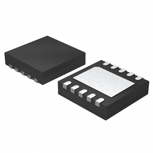
- Part No.:
- MCP33141-10T-E/MN
- Manufacturer:
- Microchip Technology
- Category:
- Analog to Digital Converters (ADC)
- Package:
- 10-WFDFN Exposed Pad
- Datasheet:
-
 MCP33141-10T-E/MN.pdf
- Description:
- IC ADC 12BIT SAR 10TDFN
- Quantity:
- Payment:

- Shipping:

Inventory:3,717
Please send an inquiry. Send us your inquiry, and we will respond immediately.
Product details
Overview
MCP33141-10T-E/MN from Microchip Technology is a 12-bit, 1 Msps single-ended SAR analog-to-digital converter with no missing codes, ultra-low standby current (1.5 µA), and integrated self-calibration for offset, gain, and linearity errors. It operates from a 1.8V analog supply (AVDD), supports digital I/O voltages from 1.7V to 5.5V (DVIO), and accepts an external reference up to 5.1V - enabling high-precision voltage measurement in battery-powered motor control and EV battery management systems.
For engineers reviewing the MCP33141-10T-E/MN datasheet, MCP33141-10T-E/MN pinout, MCP33141-10T-E/MN application, or MCP33141-10T-E/MN equivalent, this device delivers deterministic 1 µs conversion cycle time, SPI-compatible 3-wire interface with optional BUSY indicator, built-in data accumulator (up to 1024 samples), and AEC-Q100 Grade 1 qualification (-40°C to +125°C) for automotive and industrial embedded sensing.
Technical Context
The MCP33141-10T-E/MN uses a successive approximation register (SAR) architecture with internal clock generation, decoupling conversion timing from SPI clock (SCLK) rate - allowing SCLK up to 100 MHz while maintaining 1 Msps throughput. Its pseudodifferential input supports single-ended operation with full-scale range of 0V to VREF (up to 5.1V), independent of AVDD.
It features automatic power-up calibration (~500–650 ms) and on-demand recalibration via SPI command, ensuring stable INL (±0.09 LSB) and DNL (±0.05 LSB) across temperature. The device enters low-current Standby mode (~1.5 µA) between conversions, with input acquisition time of 490 ns (typ.) and conversion time of 510 ns (typ.).
Key Specifications
| Parameter | Value and Actual Design Meaning |
|---|---|
| Resolution | 12-bit with no missing codes - guarantees monotonic transfer function for closed-loop control feedback. |
| Sample Rate | 1 Msps - enables real-time sampling of fast transients in switch-mode power supplies and motor phase currents. |
| INL / DNL | ±0.09 LSB / ±0.05 LSB - ensures <0.02% full-scale linearity error for precision instrumentation-grade measurements. |
| SNR / SFDR | 73.3 dBFS / 101.4 dBc at 10 kHz - supports >12-bit effective resolution in noisy industrial environments. |
| Supply Voltages | AVDD = 1.8V; DVIO = 1.7–5.5V; VREF = up to 5.1V - allows direct interfacing with 1.8V/3.3V/5V host MCUs without level shifters. |
| Power Consumption | ~0.66 mA during conversion; ~1.5 µA in Standby - extends battery life in portable test equipment and IoT edge sensors. |
| Operating Temperature | -40°C to +125°C (AEC-Q100 Grade 1) - qualified for under-hood automotive and industrial motor drive applications. |
Pinout & Package
TDFN-10 package (3 mm × 3 mm, 0.5 mm pitch) with exposed thermal pad (EP) for enhanced thermal dissipation in high-density PCB layouts.
| Pin/Terminal | Circuit Role | Design Meaning |
|---|---|---|
| AIN+ | Analog input (single-ended) | Primary analog signal input; referenced to GND; full-scale range 0V to VREF. |
| GND | Analog/digital ground | Common reference for AVDD, DVIO, VREF, and analog input - requires low-impedance connection to minimize noise. |
| SDO | SPI serial data output | 3-state output; presents 12-bit conversion result MSB-first after CNVST falling edge; compatible with 1.7–5.5V logic. |
| SCLK | SPI serial clock input | Accepts up to 100 MHz clock; timing-independent of conversion - enables flexible host MCU clocking. |
| CNVST | Conversion start / chip select | Rising edge initiates sampling; falling edge releases SDO data - serves dual role as CS in 3-wire mode. |
| SDI | SPI serial data input | Accepts recalibration commands and configuration bits; Schmitt-triggered for noise immunity. |
| VREF | External reference voltage input | Set independently from AVDD (up to 5.1V); determines full-scale range and SNR performance. |
| AVDD | Analog supply voltage | 1.8V ±0.1V supply for SAR core and reference buffer - requires 1 µF ceramic decoupling. |
| DVIO | Digital I/O supply voltage | 1.7–5.5V supply for digital interface - supports mixed-voltage system integration. |
| EP | Exposed thermal pad | Internally connected to GND; must be soldered to PCB thermal plane for θJA = 68°C/W performance. |
Key Features
| Feature | Design Value |
|---|---|
| No latency output | Conversion result available immediately after CNVST falling edge - eliminates pipeline delay for real-time control loops. |
| Built-in data accumulator | Integrates up to 1024 consecutive samples to increase ENOB up to 18 bits - replaces external averaging firmware/hardware. |
| Self-calibration engine | Performs automatic offset/gain/linearity correction at power-up and on-demand - maintains accuracy without factory trimming. |
| Wide DVIO range | 1.7–5.5V digital interface - interoperable with PIC32, ARM Cortex-M, and other common microcontrollers without level-shifting circuitry. |
| AEC-Q100 qualification | Grade 1 (-40°C to +125°C) - validated for automotive battery monitoring, EPS, and ADAS sensor front-ends. |
Applications
| Motor Control Feedback | EV Battery Cell Monitoring |
|---|---|
|
Use Scenario: Sampling phase currents and DC-link voltage in 3-phase inverter drives. IC Role / Device Role / Timing Role: High-speed, low-latency ADC capturing transient overcurrent events at 1 Msps with deterministic timing. Use Value: Enables fast overcurrent protection (<1 µs response) and precise field-oriented control using 12-bit resolution and ±0.09 LSB INL. |
Use Scenario: Measuring individual Li-ion cell voltages in multi-cell battery packs. IC Role / Device Role / Timing Role: Precision voltage digitizer with 1.5 µA standby current and AEC-Q100 qualification for long-term reliability. Use Value: Achieves <0.02% full-scale accuracy across -40°C to +125°C, supporting ISO 26262 ASIL-B functional safety requirements. |
| Industrial Test Equipment | Switch-Mode Power Supply Sensing |
|
Use Scenario: Portable handheld multimeters and automated test fixtures requiring high SNR and low power. IC Role / Device Role / Timing Role: Primary ADC for DC voltage/current measurement with integrated accumulation and self-calibration. Use Value: Delivers 73.3 dBFS SNR and 101.4 dBc SFDR at 10 kHz, eliminating need for external anti-aliasing filters in mid-range instruments. |
Use Scenario: Real-time sensing of output voltage ripple and load-step response in DC-DC converters. IC Role / Device Role / Timing Role: High-bandwidth (45 MHz -3 dB) analog front-end digitizing fast transient waveforms. Use Value: Supports 1 Msps sampling with 2.5 ns aperture delay and 510 ns conversion time - captures sub-microsecond switching artifacts. |
Equivalent & Alternatives
The following parts are listed as comparable options for similar high-speed, low-power SAR ADC applications.
| Alternative Part | Technical Difference | Application Difference | Selection Advice |
|---|---|---|---|
| ADS7142IRUGT | 12-bit, 1 Msps, but uses internal reference (2.5V fixed); no external VREF support; lower SNR (70.5 dBFS). | Best suited for space-constrained, single-supply systems where reference flexibility is not required. | Select when board area is critical and VREF = 2.5V suffices; avoid if programmable full-scale range (0–5.1V) is needed. |
| MCP33141-05T-E/MN | Same 12-bit resolution and pinout, but 500 ksps sample rate; lower conversion current (0.33 mA) and reduced dynamic power. | Optimized for lower-bandwidth applications like temperature or pressure sensing where 1 Msps is unnecessary. | Choose for battery-powered devices prioritizing average power over speed; retains identical calibration, interface, and qualification. |
Compared with ADS7142IRUGT, the MCP33141-10T-E/MN provides wider input range via external VREF and higher SNR; compared with MCP33141-05T-E/MN, it doubles throughput at the cost of +0.33 mA active current - making it optimal for real-time control where latency matters.
Availability
MCP33141-10T-E/MN is available at Aetrix Electronics and suitable for motor control feedback, EV battery cell monitoring, and industrial test equipment requiring stable component supply, AEC-Q100 compliance, and long-term production continuity.
Supply support for MCP33141-10T-E/MN includes scheduled delivery planning, volume procurement assistance, BOM continuity management, traceable sourcing, and lifecycle availability coordination for OEM customers, industrial embedded developers, connected-device designers, and electronics production programs.
Manufacturer
Microchip Technology is a global semiconductor company specializing in microcontrollers, analog, and interface ICs, with leadership in embedded control and automotive-qualified components.
The MCP331xx family is designed for high-precision, low-power data acquisition in automotive, industrial, and energy-efficient embedded systems - emphasizing speed, accuracy, and robustness across extreme temperatures.
FAQ
What is the maximum external reference voltage supported by the MCP33141-10T-E/MN?
The MCP33141-10T-E/MN supports an external reference voltage (VREF) up to 5.1V, independent of the 1.8V AVDD supply. This allows full-scale input ranges from 0V to 5.1V, enabling direct measurement of standard industrial signals without external amplification or attenuation. Operation at VREF = 5.1V achieves optimal SNR (73.3 dBFS) and SFDR (101.4 dBc) at 10 kHz input frequency.
Does the MCP33141-10T-E/MN require external level-shifting when interfacing with a 5V microcontroller?
No, the MCP33141-10T-E/MN does not require external level-shifting when interfacing with a 5V microcontroller. Its DVIO pin accepts digital I/O voltages from 1.7V to 5.5V, and all digital inputs (CNVST, SCLK, SDI) are Schmitt-triggered with hysteresis. The SDO output is 5V-tolerant and drives valid logic levels across the full DVIO range - simplifying design with mixed-voltage hosts like PIC32MZ or STM32H7.
How does the built-in data accumulator improve measurement resolution in the MCP33141-10T-E/MN?
The built-in data accumulator in the MCP33141-10T-E/MN integrates up to 1024 consecutive 12-bit conversion results and outputs the averaged value - increasing effective number of bits (ENOB) up to 18 bits. This reduces quantization noise without firmware overhead or external DSP, enabling high-resolution DC measurements (e.g., battery voltage drift) while retaining the device's 1 Msps native speed for transient capture.
What is the typical power consumption of the MCP33141-10T-E/MN during conversion and standby modes?
The MCP33141-10T-E/MN consumes ~0.66 mA (660 µA) during active conversion at 1 Msps and only ~1.5 µA in Standby mode - where sampling capacitors remain connected to the input for fast wake-up. Total power dissipation is ~3.6 mW at 1 Msps (including AVDD, DVIO, and VREF currents), dropping to ~3.3 µW in Standby. This ultra-low quiescent current makes it ideal for always-on battery monitoring nodes.
Is the MCP33141-10T-E/MN pin-compatible with other devices in the MCP331xx family?
Yes, the MCP33141-10T-E/MN is pin-compatible with MCP33151-10T-E/MN, MCP33141-05T-E/MN, and MCP33151-05T-E/MN in the same TDFN-10 package. All share identical pinout, interface protocol, and supply requirements - allowing hardware reuse across 12-/14-bit and 500 ksps/1 Msps variants. Firmware changes are limited to timing and resolution handling.
MCP33141-10T-E/MN Specifications
- Product attributes
- Attribute value
- Manufacturer:
- Microchip Technology
- Series:
- -
- Package/Case:
- 10-WFDFN Exposed Pad
- Packaging:
- Tape & Reel (TR)
- Product Status:
- Active
- Number of Bits:
- 12
- Sampling Rate (Per Second):
- 1M
- Number of Inputs:
- 1
- Input Type:
- Single Ended
- Data Interface:
- SPI
- Configuration:
- ADC
- Ratio - S/H:ADC:
- 0:1
- Number of A/D Converters:
- 1
- Architecture:
- SAR
- Reference Type:
- External
- Voltage - Supply, Analog:
- 1.7V ~ 1.9V
- Voltage - Supply, Digital:
- 1.7V ~ 5.5V
- Features:
- -
- Operating Temperature:
- -40°C ~ 125°C
- Supplier Device Package:
- 10-TDFN (3x3)
- Mounting Type:
- Surface Mount
- Grade:
- Automotive
- Qualification:
- AEC-Q100
MCP33141-10T-E/MN FAQ
1.How can I place an order for MCP33141-10T-E/MN through Aetrix?
Please submit a Request for Quotation (RFQ) for MCP33141-10T-E/MN on Aetrix. Our sales agent will provide a competitive quotation and guide you through the order confirmation once you accept the terms.
2.Are the price and stock information for MCP33141-10T-E/MN reliable?
The price and inventory of MCP33141-10T-E/MN are updated periodically and may fluctuate due to market conditions. Stock and pricing data are typically refreshed every 24 hours. Quotation validity for MCP33141-10T-E/MN is usually 5 days.
3.What payment methods are accepted for MCP33141-10T-E/MN?
We accept Wire Transfer, PayPal, Credit Card, Western Union, MoneyGram, and Escrow for MCP33141-10T-E/MN transactions.
Note: Certain payment methods may incur a processing fee.
4.How is shipping managed for MCP33141-10T-E/MN?
MCP33141-10T-E/MN orders can be shipped via leading logistics carriers, including DHL, UPS, FedEx, TNT, or Registered Mail.
Once your MCP33141-10T-E/MN order is processed, you will receive an email with the shipment details and tracking number.
Note: Tracking information may take up to 24 hours to appear. Express delivery typically takes 3–5 business days.
5.How can I obtain technical support or documentation for MCP33141-10T-E/MN?
For technical support, including MCP33141-10T-E/MN datasheets, pinout diagrams, or application guidance, please contact our engineering support team. They can provide detailed documentation and assistance for your MCP33141-10T-E/MN requirements.
6.How does Aetrix verify that MCP33141-10T-E/MN is sourced from the original manufacturer or authorized distributors?
All MCP33141-10T-E/MN products on Aetrix are procured from qualified distributors and authorized channels. Our dedicated quality assurance team conducts strict verification, including traceability checks and, if necessary, third-party testing. This ensures that MCP33141-10T-E/MN meets industry standards.
7.What is the process for return or replacement of MCP33141-10T-E/MN?
All MCP33141-10T-E/MN units undergo pre-shipment inspection (PSI). If there is an issue with MCP33141-10T-E/MN, returns or replacements are accepted under the following conditions:
1.Quantity discrepancies, incorrect items, or visible external defects (such as breakage or corrosion), acknowledged by Aetrix.
2.The issue is reported within 90 days of delivery.
3.The MCP33141-10T-E/MN part is unused and in its original packaging.
Return procedure for MCP33141-10T-E/MN:
1.Submit a request within 90 days.
2.Obtain a Return Material Authorization (RMA) from Aetrix.
MCP33141-10T-E/MN Tags
-
ADC081C021CIMKX/NOPB
Texas Instruments

-
MCP3021A5T-E/OT
Microchip Technology
-
TLA2024IRUGR
Texas Instruments
-
MCP3221A5T-E/OT
Microchip Technology
-
MCP3221A5T-I/OT
Microchip Technology
-
MCP3221A4T-E/OT
Microchip Technology
-
MCP3221A6T-E/OT
Microchip Technology
-
MCP3221A0T-E/OT
Microchip Technology
-
MCP3221A1T-E/OT
Microchip Technology

-
ADC121S021CIMFX/NOPB
Texas Instruments

-
MCP3001-I/MS
Microchip Technology

-
MCP3001-I/SN
Microchip Technology
Tech Hub

A practical engineering and sourcing framework covering lifecycle verification, lifetime-buy calculations, replacement qualification, supplier checks and counterfeit-risk controls.

TTL and CMOS logic families differ in thresholds, loading, output drive, power and timing. This engineering guide compares 74HC and 74HCT, calculates noise margins and checks 3.3 V/5 V compatibility.

A practical engineering guide to 3.3V and 5V logic compatibility, input thresholds, resistor dividers, translator ICs, MOSFET level shifting, I2C pull-ups, timing limits and power-sequencing risks.

The 74HC595 uses push-pull logic outputs, while the TPIC6B595 uses 50 V open-drain DMOS sinks for higher-power loads. This guide compares timing, current limits, 3.3 V interfacing, load wiring, thermal…

The 74HC595 converts serial data into eight stable parallel outputs. This guide covers pin functions, shift and storage timing, OE and MR behavior, drive-current limits, cascading, voltage compatibilit…

A technical comparison of level-sensitive latches and edge-triggered flip-flops, covering timing windows, setup and hold limits, master–slave operation, time borrowing, race-through, HDL inference and…

A D latch stores one bit while Enable controls when data can pass. This reference covers gate-level operation, truth tables, transparency, setup and hold timing, LE versus OE, common ICs and practical …

An SR latch stores one bit through cross-coupled feedback. This engineering reference covers NOR and NAND implementations, truth tables, forbidden-state recovery, gated operation, switch debouncing, fa…

Latch circuits retain one bit through feedback. This technical reference covers SR and D latches, truth tables, transparency, timing limits, latch-versus-flip-flop behavior, applications and common log…

An engineering guide to LED driver operation, constant-current and constant-voltage outputs, linear and switching topologies, dimming, IC selection, calculations, replacement compatibility, and fault c…


