
 My Inquiry
 My Account


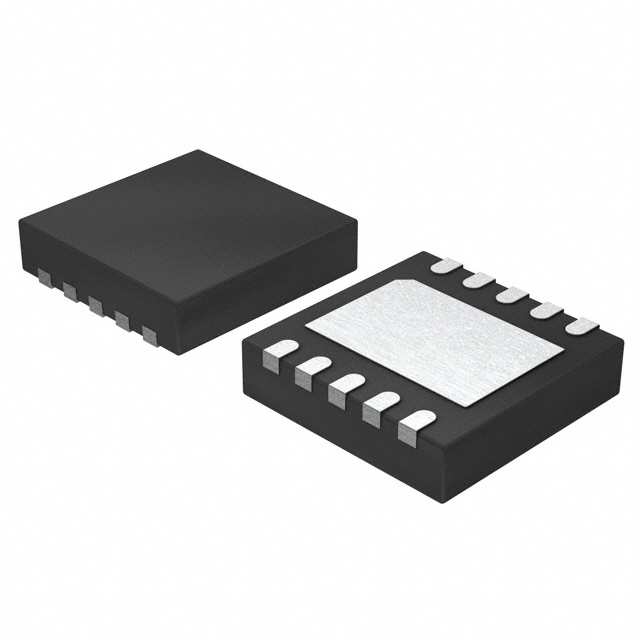
Microchip Technology MCP73113-06SI/MF
- Part No.:
- MCP73113-06SI/MF
- Manufacturer:
- Microchip Technology
- Category:
- Battery Chargers
- Package:
- 10-VFDFN Exposed Pad
- Datasheet:
-
 MCP73113-06SI/MF.pdf
- Description:
- IC BATT CHG LI-ION 1CELL 10DFN
- Quantity:
- Payment:

- Shipping:

Inventory:288
Please send an inquiry. Send us your inquiry, and we will respond immediately.
Product details
Overview
MCP73113-06SI/MF from Microchip Technology is a single-cell Li-ion/Li-polymer linear battery charge management controller with integrated pass transistor, current sense, input overvoltage protection (6.5 V), and reverse discharge protection. It delivers 4.20 V regulated charge voltage ±0.5% over –5°C to +55°C, supports 130–1100 mA resistor-programmable fast charge current, and operates across –40°C to +85°C in space-constrained portable devices.
For engineers reviewing the MCP73113-06SI/MF datasheet, MCP73113-06SI/MF pinout, MCP73113-06SI/MF application, or MCP73113-06SI/MF equivalent, this page provides verified technical context, validated pin functions, confirmed charge algorithm behavior (CC/CV with thermal regulation), factory-set 4.20 V / 6.5 V OVP / 10% preconditioning / 32-min timer / 6-hr elapse safety timer / 10% end-of-charge threshold / 95% auto-recharge, and DFN-10 package implementation details.
Technical Context
The MCP73113-06SI/MF implements a fully integrated linear charging architecture with internal P-channel MOSFET pass element (350 mΩ typical RDS(on)), precision voltage reference (1.21 V), and dual-loop control: constant-current regulation via PROG pin resistor feedback and constant-voltage regulation at factory-trimmed 4.20 V with ±0.5% tolerance across temperature.
Its protection stack includes input overvoltage lockout (6.5 V start, 150 mV hysteresis), undervoltage lockout (4.15 V start, 100 mV hysteresis), thermal regulation (current reduction above ~105°C), thermal shutdown (150°C trip, 10°C hysteresis), and battery short-circuit detection (1.7 V threshold, 25 mA recovery current).
Key Specifications
| Parameter | Value and Actual Design Meaning |
|---|---|
| Charge Voltage | 4.20 V ±0.5% over –5°C to +55°C - ensures safe, full-capacity charging of standard Li-ion cells without overvoltage risk. |
| Input OVP Threshold | 6.5 V (MCP73113 variant) - protects against wall-adapter spikes and enables use with low-cost 5 V supplies subject to transient overshoot. |
| Fast Charge Current Range | 130–1100 mA via external PROG resistor - allows flexible design for 800–2000 mAh batteries with minimal BOM count. |
| Preconditioning | Enabled at 10% of IREG, 71.5% VREG threshold, 32-minute timer - safely recovers deeply depleted cells before CC mode. |
| End-of-Charge Termination | 10% IREG minimum current ratio - balances full charge completion against excessive time in CV phase for cycle life. |
| Auto-Recharge Threshold | 95% of VREG (i.e., 3.99 V) - triggers recharge when battery self-discharge drops voltage below safe operating level. |
| Package | DFN-10 (3 mm × 3 mm) with exposed thermal pad - enables high-power dissipation in ultra-compact footprint for handhelds. |
Pinout & Package
Package: 10-lead DFN (3 mm × 3 mm) with exposed thermal pad (EP); EP must be soldered to PCB copper for thermal performance.
| Pin/Terminal | Circuit Role | Design Meaning |
|---|---|---|
| VDD (Pins 1, 2) | Battery management input supply | Accepts 4.2–6.5 V input; absolute max 18 V; powers internal circuitry and gate drive; bypass required with ≥1 µF to VSS. |
| VBAT (Pins 3, 4) | Battery charge control output | Drain of internal P-MOSFET; connects directly to battery anode; regulates voltage/current; requires ≥1 µF bypass to VSS. |
| NC (Pins 5, 6) | No connect | Unbonded pins; must remain unconnected per datasheet; no routing or stitching allowed. |
| STAT (Pin 7) | Status output | Open-drain logic output; low during active charge (precondition, CC, CV); high-Z at shutdown, standby, or charge complete (Type 1). |
| VSS (Pins 8, 9) | Ground reference | Common return for battery cathode, input supply negative, and all internal bias circuits; must be low-impedance star point. |
| PROG (Pin 10) | Current regulation & enable | Resistor-to-VSS sets fast charge current; floating or >200 kΩ disables charger; also serves as enable pin. |
| EP (Pin 11) | Exposed thermal pad | Internally connected to VSS; must be soldered to large PCB copper pour with multiple thermal vias for junction temp control. |
Key Features
| Feature | Design Value |
|---|---|
| Integrated pass transistor | Internal P-channel MOSFET (350 mΩ RDS(on)) eliminates external FET, reducing board area and component count. |
| Factory-trimmed voltage regulation | 4.20 V ±0.5% over –5°C to +55°C - eliminates need for external voltage-setting resistors or calibration. |
| Input overvoltage protection | 6.5 V OVP with 150 mV hysteresis - prevents damage from adapter transients without external TVS diodes. |
| Thermal regulation + shutdown | Gradual current reduction above ~105°C + hard shutdown at 150°C - maintains reliability under high ambient or poor heatsinking. |
| Preconditioning & safety timers | 32-minute precondition timer + 6-hour elapsed safety timer - prevents indefinite trickle charge and thermal runaway. |
| Reverse discharge protection | Blocks battery-to-input current flow when VDD is absent - preserves battery charge during system standby or adapter removal. |
Applications
| USB-Powered Portable Media Player | Digital Still Camera Charger |
|---|---|
Use Scenario: Compact camera powered by single-cell Li-ion battery, charged via USB 5 V adapter with variable load and ambient temperature swings. IC Role / Device Role / Timing Role: Linear charge controller managing CC/CV profile, OVP, UVLO, and thermal regulation; STAT pin drives LED indicator. Use Value: Enables reliable full-charge completion within 2.5 hours using 500 mA fast charge while preventing overvoltage damage from low-cost USB adapters. |
Use Scenario: High-resolution digital camera requiring stable 4.20 V battery voltage and automatic top-up after partial discharge during photo bursts. IC Role / Device Role / Timing Role: Battery management IC executing precondition → fast charge → CV → termination → auto-recharge sequence with 95% VREG trigger. Use Value: Delivers consistent runtime across 500+ charge cycles by maintaining precise 4.20 V regulation and avoiding overcharge stress. |
| Bluetooth Headset Charging Circuit | MP3 Player Wall Adapter Interface |
Use Scenario: Ultra-low-power Bluetooth headset with 300 mAh battery, frequently charged via intermittent USB power with tight space constraints. IC Role / Device Role / Timing Role: Integrated linear charger providing 130 mA fast charge, 10% preconditioning, and 32-min safety timer in DFN-10 package. Use Value: Achieves <1.5 mm profile height and <30 mm² board area while ensuring safe recovery of deeply discharged cells. |
Use Scenario: Cost-sensitive MP3 player using unregulated 5 V wall adapter prone to 100–200 mV ripple and occasional 7–8 V spikes. IC Role / Device Role / Timing Role: Input-protected linear charger with 6.5 V OVP, 4.15 V UVLO, and soft-start to suppress inrush into 100 µF output cap. Use Value: Eliminates need for external OVP IC or TVS, reducing BOM cost by $0.12 and improving long-term adapter compatibility. |
Equivalent & Alternatives
The following parts are listed as comparable options for similar single-cell Li-ion linear charge management applications.
| Alternative Part | Technical Difference | Application Difference | Selection Advice |
|---|---|---|---|
| MCP73113-16SI/MF | Factory-set 4.10 V charge voltage, same 6.5 V OVP, 10% preconditioning, 32-min timer, 6-hr elapse timer, 10% termination, 95% auto-recharge. | Suitable for legacy Li-ion cells requiring lower termination voltage to extend cycle life at expense of capacity. | Select when battery chemistry specifies 4.10 V nominal full-charge voltage and thermal margin is prioritized over runtime. |
| MCP73114-0NSI/MF | Same 4.20 V charge voltage but 5.8 V OVP threshold; identical preconditioning, timer, termination, and auto-recharge settings. | Required for systems where input supply may exceed 6.0 V but must remain below 5.8 V OVP threshold (e.g., regulated 5.5 V sources). | Choose when tighter input voltage control exists and 6.5 V OVP is unnecessarily conservative for the power supply design. |
Compared with MCP73113-16SI/MF and MCP73114-0NSI/MF, the MCP73113-06SI/MF uniquely balances 4.20 V capacity optimization with 6.5 V OVP robustness for unregulated 5 V adapters - making it optimal for cost-sensitive consumer electronics where both runtime and spike resilience matter.
Availability
MCP73113-06SI/MF is available at Aetrix Electronics and suitable for USB chargers, digital still cameras, Bluetooth headsets, and portable media players requiring stable component supply, long-lifecycle support, and guaranteed traceable sourcing.
Supply support for MCP73113-06SI/MF includes scheduled delivery planning, volume procurement assistance, BOM continuity management, traceable sourcing, and lifecycle availability coordination for OEM customers, industrial embedded developers, connected-device designers, and electronics production programs.
Manufacturer
Microchip Technology Inc. is a leading provider of microcontroller, analog, FPGA, and mixed-signal semiconductors, headquartered in Chandler, Arizona, with global design and manufacturing operations.
The MCP73113/4 product line was designed specifically for space-constrained, cost-sensitive portable electronics requiring fully integrated, single-chip Li-ion charging with factory-trimmed accuracy and comprehensive protection - eliminating external components while meeting IEC 62368-1 safety requirements.
FAQ
What is the factory-set charge voltage and OVP threshold for MCP73113-06SI/MF?
The MCP73113-06SI/MF is factory-configured for 4.20 V battery regulation voltage with ±0.5% tolerance over –5°C to +55°C and 6.5 V input overvoltage protection (OVP) start threshold with 150 mV hysteresis. These values are laser-trimmed during production and cannot be modified externally - they define the core charging behavior of the MCP73113-06SI/MF in all operating conditions.
How does the PROG pin function in MCP73113-06SI/MF beyond setting charge current?
In addition to programming fast charge current via an external resistor to VSS, the PROG pin on the MCP73113-06SI/MF serves as the primary enable/disable control: floating the pin or connecting it to impedance >200 kΩ places the MCP73113-06SI/MF into shutdown mode with zero quiescent current (≤5 µA), while pulling it to VSS below 100 mV initiates charging - enabling simple hardware-based charge control without a microcontroller.
What thermal protection mechanisms does MCP73113-06SI/MF implement?
The MCP73113-06SI/MF features two-tier thermal protection: first, continuous thermal regulation that gradually reduces charge current above ~105°C to maintain safe junction temperature; second, hard thermal shutdown at 150°C (±5°C) with 10°C hysteresis that suspends all charging until die cools - both mechanisms are implemented in silicon and require no external components, ensuring reliability of the MCP73113-06SI/MF under sustained high-power or high-ambient conditions.
Can MCP73113-06SI/MF be used with batteries requiring 4.35 V or 4.40 V charge voltage?
No - the MCP73113-06SI/MF is factory-trimmed exclusively for 4.20 V regulation and cannot be reconfigured for 4.35 V or 4.40 V operation. For those voltages, Microchip offers distinct part numbers: MCP73113-25SI/MF (4.35 V) and MCP73113-30SI/MF (4.40 V). Using MCP73113-06SI/MF with higher-voltage cells risks undercharging and reduced capacity, while forcing voltage adjustment violates the MCP73113-06SI/MF's fixed internal reference architecture.
What is the role of the NC pins (5 and 6) on the MCP73113-06SI/MF DFN-10 package?
Pins 5 and 6 of the MCP73113-06SI/MF are designated No Connect (NC) - they are physically present but internally unbonded and electrically isolated. Per Microchip's datasheet DS20002183E, these pins must remain unconnected on the PCB; routing traces to them, applying solder mask openings, or using them for mechanical anchoring violates the MCP73113-06SI/MF's qualified layout and may compromise thermal performance or ESD robustness.
MCP73113-06SI/MF Specifications
- Product attributes
- Attribute value
- Manufacturer:
- Microchip Technology
- Series:
- -
- Package/Case:
- 10-VFDFN Exposed Pad
- Packaging:
- Tube
- Product Status:
- Active
- Battery Chemistry:
- Lithium Ion/Polymer
- Number of Cells:
- 1
- Current - Charging:
- Constant - Programmable
- Programmable Features:
- -
- Fault Protection:
- Over Voltage
- Charge Current - Max:
- 1.1A
- Battery Pack Voltage:
- 4.2V
- Voltage - Supply (Max):
- 6.5V
- Interface:
- -
- Operating Temperature:
- -40°C ~ 85°C (TA)
- Grade:
- -
- Qualification:
- -
- Mounting Type:
- Surface Mount
- Supplier Device Package:
- 10-DFN (3x3)
MCP73113-06SI/MF FAQ
1.How can I place an order for MCP73113-06SI/MF through Aetrix?
Please submit a Request for Quotation (RFQ) for MCP73113-06SI/MF on Aetrix. Our sales agent will provide a competitive quotation and guide you through the order confirmation once you accept the terms.
2.Are the price and stock information for MCP73113-06SI/MF reliable?
The price and inventory of MCP73113-06SI/MF are updated periodically and may fluctuate due to market conditions. Stock and pricing data are typically refreshed every 24 hours. Quotation validity for MCP73113-06SI/MF is usually 5 days.
3.What payment methods are accepted for MCP73113-06SI/MF?
We accept Wire Transfer, PayPal, Credit Card, Western Union, MoneyGram, and Escrow for MCP73113-06SI/MF transactions.
Note: Certain payment methods may incur a processing fee.
4.How is shipping managed for MCP73113-06SI/MF?
MCP73113-06SI/MF orders can be shipped via leading logistics carriers, including DHL, UPS, FedEx, TNT, or Registered Mail.
Once your MCP73113-06SI/MF order is processed, you will receive an email with the shipment details and tracking number.
Note: Tracking information may take up to 24 hours to appear. Express delivery typically takes 3–5 business days.
5.How can I obtain technical support or documentation for MCP73113-06SI/MF?
For technical support, including MCP73113-06SI/MF datasheets, pinout diagrams, or application guidance, please contact our engineering support team. They can provide detailed documentation and assistance for your MCP73113-06SI/MF requirements.
6.How does Aetrix verify that MCP73113-06SI/MF is sourced from the original manufacturer or authorized distributors?
All MCP73113-06SI/MF products on Aetrix are procured from qualified distributors and authorized channels. Our dedicated quality assurance team conducts strict verification, including traceability checks and, if necessary, third-party testing. This ensures that MCP73113-06SI/MF meets industry standards.
7.What is the process for return or replacement of MCP73113-06SI/MF?
All MCP73113-06SI/MF units undergo pre-shipment inspection (PSI). If there is an issue with MCP73113-06SI/MF, returns or replacements are accepted under the following conditions:
1.Quantity discrepancies, incorrect items, or visible external defects (such as breakage or corrosion), acknowledged by Aetrix.
2.The issue is reported within 90 days of delivery.
3.The MCP73113-06SI/MF part is unused and in its original packaging.
Return procedure for MCP73113-06SI/MF:
1.Submit a request within 90 days.
2.Obtain a Return Material Authorization (RMA) from Aetrix.
MCP73113-06SI/MF Tags

-
BQ21040DBVR
Texas Instruments

-
MCP73812T-420I/OT
Microchip Technology
-
MCP73831T-2ACI/OT
Microchip Technology
-
MCP73832T-2ACI/OT
Microchip Technology
-
MCP73831T-2DCI/OT
Microchip Technology
-
MCP73832T-2DCI/OT
Microchip Technology
-
MCP73831T-2ATI/OT
Microchip Technology
-
MCP73832T-2ATI/OT
Microchip Technology
-
MCP73831T-5ACI/OT
Microchip Technology

-
MCP73832T-2ACI/MC
Microchip Technology
-
MCP73831T-2ACI/MC
Microchip Technology
-
MCP73831T-2ATI/MC
Microchip Technology
Tech Hub

TTL and CMOS logic families differ in thresholds, loading, output drive, power and timing. This engineering guide compares 74HC and 74HCT, calculates noise margins and checks 3.3 V/5 V compatibility.

A practical engineering guide to 3.3V and 5V logic compatibility, input thresholds, resistor dividers, translator ICs, MOSFET level shifting, I2C pull-ups, timing limits and power-sequencing risks.

The 74HC595 uses push-pull logic outputs, while the TPIC6B595 uses 50 V open-drain DMOS sinks for higher-power loads. This guide compares timing, current limits, 3.3 V interfacing, load wiring, thermal…

The 74HC595 converts serial data into eight stable parallel outputs. This guide covers pin functions, shift and storage timing, OE and MR behavior, drive-current limits, cascading, voltage compatibilit…

A technical comparison of level-sensitive latches and edge-triggered flip-flops, covering timing windows, setup and hold limits, master–slave operation, time borrowing, race-through, HDL inference and…

A D latch stores one bit while Enable controls when data can pass. This reference covers gate-level operation, truth tables, transparency, setup and hold timing, LE versus OE, common ICs and practical …

An SR latch stores one bit through cross-coupled feedback. This engineering reference covers NOR and NAND implementations, truth tables, forbidden-state recovery, gated operation, switch debouncing, fa…

Latch circuits retain one bit through feedback. This technical reference covers SR and D latches, truth tables, transparency, timing limits, latch-versus-flip-flop behavior, applications and common log…

An engineering guide to LED driver operation, constant-current and constant-voltage outputs, linear and switching topologies, dimming, IC selection, calculations, replacement compatibility, and fault c…

Operational amplifier guide covering op amp basics, feedback, ideal vs real op amps, common configurations, buffer circuits, offset, bias current, gain-bandwidth, slew rate, rail-to-rail limits and sel…


