
 My Inquiry
 My Account


Microchip Technology MCP73833-NVI/UN
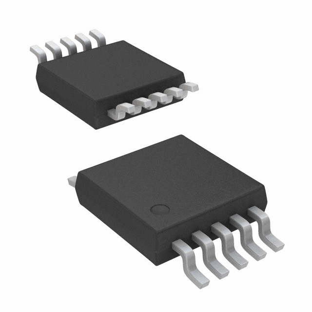
- Part No.:
- MCP73833-NVI/UN
- Manufacturer:
- Microchip Technology
- Category:
- Battery Chargers
- Package:
- 10-TFSOP, 10-MSOP (0.118", 3.00mm Width)
- Datasheet:
-
 MCP73833-NVI/UN.pdf
- Description:
- IC BATT CNTRL LI-ION 1CEL 10MSOP
- Quantity:
- Payment:

- Shipping:

Inventory:495
Please send an inquiry. Send us your inquiry, and we will respond immediately.
Product details
Overview
MCP73833-NVI/UN from Microchip Technology is a stand-alone linear Li-ion/Li-polymer battery charge management controller in a 10-lead DFN-10 (3 mm × 3 mm) package. It delivers constant-current/constant-voltage charging with thermal regulation, 4.20 V ±0.75% voltage regulation, up to 1 A programmable charge current via external resistor, and integrated reverse discharge protection - designed for USB-powered portable devices including Bluetooth headsets and digital cameras.
For engineers reviewing the MCP73833-NVI/UN datasheet, MCP73833-NVI/UN pinout, MCP73833-NVI/UN application, or MCP73833-NVI/UN equivalent, key selection criteria include its factory-set 4.20 V regulation, thermal foldback behavior at >105°C junction temperature, dual open-drain STAT outputs, PG (power-good) indication, and thermistor-based temperature monitoring with 1.23 V / 0.25 V thresholds.
Technical Context
The MCP73833-NVI/UN implements a fully autonomous linear charging algorithm with preconditioning (trickle charge), fast-charge CC mode, CV regulation, and automatic recharge - all governed by internal comparators and a 4–8 hour safety timer. Its integrated P-channel MOSFET pass transistor features 300 mΩ typical RDS(on), enabling efficient low-dropout operation with minimal external components.
Thermal regulation dynamically reduces charge current above ~105°C junction temperature, while thermal shutdown halts charging at 150°C with 10°C hysteresis. The device supports system test (LDO) mode when THERM is driven > (VDD − 100 mV), delivering regulated output at the selected VREG with current limit set by PROG.
Key Specifications
| Parameter | Value and Actual Design Meaning |
|---|---|
| Voltage Regulation | 4.20 V ±0.75% - factory-trimmed reference ensures accurate full-charge termination for standard Li-ion cells. |
| Max Charge Current | 1000 mA - programmable via 1.0 kΩ PROG-to-VSS resistor; enables compact single-cell charging in space-constrained designs. |
| Thermal Regulation Threshold | 105°C typical - begins linear current reduction before thermal shutdown, preserving charge time and reliability under high ambient or power dissipation. |
| Preconditioning Threshold | 66.5% of VREG (≈2.79 V) - initiates trickle charge for deeply depleted batteries, preventing damage from excessive initial current. |
| Charge Termination Ratio | 5% of IREG - ends fast charge when average current drops to 50 mA (at 1 A setting), ensuring safe saturation without overcharge. |
| THERM Bias Current | 50 µA ±6% - stable current source for 10 kΩ NTC thermistors, enabling accurate battery temperature monitoring across -40°C to +85°C. |
| UVLO Threshold | 3.55 V (typical start), 3.45 V (stop) - prevents operation below safe input voltage and blocks reverse discharge when VDD falls near VBAT. |
Pinout & Package
Package: DFN-10 (3 mm × 3 mm), exposed thermal pad (EP) electrically connected to VSS. Requires soldering EP to PCB ground plane for thermal performance and electrical integrity.
| Pin/Terminal | Circuit Role | Design Meaning |
|---|---|---|
| VDD (Pins 1,2) | Battery management input supply | Accepts 3.75–6 V input; powers internal circuitry and enables charging only above UVLO threshold (3.55 V). |
| STAT1, STAT2 (Pins 3,4) | Open-drain charge status outputs | Drive LEDs or microcontroller inputs: STAT1 = low during charge, STAT2 = low at end-of-charge; both high-impedance in shutdown. |
| VSS (Pin 5) | 0 V reference | Common return for battery negative, input supply, PROG resistor, and EP connection - must be low-impedance ground path. |
| PROG (Pin 6) | Current regulation set and enable | Resistor to VSS sets fast-charge current (IREG = 1000 V/RPROG); floating disables charger and limits reverse discharge to <2 µA. |
| PG (Pin 7) | Power-good indicator | Pseudo open-drain output pulled low when VDD > UVLO and VDD > VBAT - signals valid input power presence to host systems. |
| THERM (Pin 8) | Thermistor input | 50 µA bias current source; compares voltage against 1.23 V / 0.25 V thresholds to suspend charging outside safe temperature range. |
| VBAT (Pins 9,10) | Battery charge control output | Drain of internal P-MOSFET; connects directly to battery positive; requires ≥1 µF ceramic bypass capacitor for stability. |
| EP (Pin 11) | Exposed thermal pad | Internally tied to VSS - must be soldered to PCB ground plane to achieve θJA = 41°C/W and sustain full 1 A operation. |
Key Features
| Feature | Design Value |
|---|---|
| Integrated pass transistor | Eliminates external MOSFET and gate driver, reducing BOM count and PCB area in portable USB chargers. |
| Thermal regulation with foldback | Automatically scales down charge current above 105°C junction temperature - maintains safe operation without external thermal sensors. |
| Factory-set 4.20 V regulation | Meets JEITA-compliant charging for standard Li-ion cells without external feedback resistors or trimming. |
| Dual STAT outputs with defined states | Enables discrete LED status indication (charging vs. complete) or direct GPIO interface to MCU without additional logic. |
| Reverse discharge protection | Blocks battery-to-input leakage (<2 µA) when VDD is absent - preserves battery life in always-connected USB devices. |
| System test (LDO) mode | Allows VBAT to regulate at 4.20 V without battery present - simplifies system-level functional testing during production. |
Applications
| USB-Powered Portable Devices | Bluetooth Audio Accessories |
|---|---|
Use Scenario: Charging compact Li-ion batteries from 5 V USB ports in smartphones, power banks, and wearables. IC Role / Device Role / Timing Role: Stand-alone linear charge controller managing CC/CV profile, thermal safety, and end-of-charge signaling. Use Value: Enables certified USB compliance with <1 A draw, no external pass element, and automatic power-down when USB is unplugged. | Use Scenario: Powering and recharging Bluetooth headsets and earbuds with tight space constraints and thermal sensitivity. IC Role / Device Role / Timing Role: Battery management IC providing preconditioning for deeply discharged cells and automatic recharge on voltage sag. Use Value: Extends usable battery life per cycle by avoiding deep discharge damage and enabling seamless top-up charging. |
| Digital Imaging Equipment | Personal Data Assistants |
Use Scenario: Recharging Li-polymer batteries in digital cameras and camcorders requiring stable voltage regulation and temperature monitoring. IC Role / Device Role / Timing Role: Integrated charger with thermistor interface and 4.20 V ±0.75% regulation for precise cell voltage control. Use Value: Prevents overvoltage stress on sensitive imaging sensors and memory by maintaining strict CV tolerance during final charge phase. | Use Scenario: Managing battery charging in handheld PDAs and early-generation tablets with limited board area and no host processor supervision. IC Role / Device Role / Timing Role: Autonomous charge controller with dual STAT outputs and PG signal for user-visible status and system power sequencing. Use Value: Delivers full charge management without firmware intervention - ideal for cost-sensitive, resource-limited embedded systems. |
Equivalent & Alternatives
The following parts are listed as comparable options for similar linear Li-ion charge management applications.
| Alternative Part | Technical Difference | Application Difference | Selection Advice |
|---|---|---|---|
| BQ24075RGTR | Fixed 4.2 V regulation, 1.5 A max current, integrated LDO, no PG output, different pinout (QFN-16). | Supports higher current and system power path but lacks power-good signaling and has larger footprint. | Select BQ24075RGTR when >1 A charge current or integrated LDO for system rail is required; verify PCB layout compatibility. |
| MCP73831T-2DCI/OT | Single-pin PROG variant (SOT-23-5), 500 mA max, same 4.20 V regulation, no PG or THERM pins. | Ultra-compact solution for cost-sensitive, low-current applications where temperature monitoring and power-good are not needed. | Select MCP73831T-2DCI/OT for space-constrained designs with ≤500 mA requirement and simplified thermal/safety needs. |
Compared with BQ24075RGTR and MCP73831T-2DCI/OT, the MCP73833-NVI/UN uniquely balances 1 A capability, PG signaling, thermistor support, and DFN-10 compactness - making it optimal for mid-tier USB-charged portable devices needing full safety and status visibility without host MCU coordination.
Availability
MCP73833-NVI/UN is available at Aetrix Electronics and suitable for USB-powered portable devices, Bluetooth audio accessories, digital imaging equipment, and personal data assistants requiring stable component supply and long-term industrial availability.
Supply support for MCP73833-NVI/UN includes scheduled delivery planning, volume procurement assistance, BOM continuity management, traceable sourcing, and lifecycle availability coordination for OEM customers, industrial embedded developers, connected-device designers, and electronics production programs.
Manufacturer
Microchip Technology is a U.S.-based semiconductor manufacturer specializing in microcontrollers, analog, interface, and power management ICs for embedded control applications.
The MCP7383x family was designed specifically for cost-sensitive, space-constrained Li-ion/Li-polymer charging in portable consumer electronics - emphasizing integration, thermal robustness, and USB compliance without host processor dependency.
FAQ
What is the factory-set voltage regulation for MCP73833-NVI/UN?
The MCP73833-NVI/UN is factory-trimmed to 4.20 V ±0.75% constant-voltage regulation, optimized for standard single-cell Li-ion batteries. This value is fixed and cannot be adjusted externally - unlike other variants in the MCP73833/4 family offering 4.35 V, 4.40 V, or 4.50 V options. The MCP73833-NVI/UN datasheet confirms this specification in Section 1.0 Electrical Characteristics under "Regulated Output Voltage" with typical 4.20 V and min/max bounds of 4.168 V and 4.232 V.
How does the MCP73833-NVI/UN handle thermal regulation during charging?
The MCP73833-NVI/UN implements analog thermal regulation that begins reducing charge current linearly when the die junction temperature exceeds approximately 105°C, as specified in the DS22005B datasheet. This foldback behavior continues until thermal shutdown activates at 150°C. Unlike digital thermal throttling, this analog response avoids abrupt current steps, maintaining smoother charge progression while protecting reliability. The DFN-10 package's low θJA of 41°C/W supports sustained 1 A operation when the exposed pad (EP) is properly soldered to a thermal ground plane.
What is the function of the PG pin on the MCP73833-NVI/UN?
The PG (Power Good) pin on the MCP73833-NVI/UN is a pseudo open-drain output that sinks current when VDD is above the UVLO threshold (≥3.55 V) and exceeds the battery voltage (VBAT). It remains low during active charging and charge-complete states, signaling valid input power presence to host systems. Because PG has an internal diode path back to VDD, it must only be pulled up to the VDD rail - not to a separate logic supply. This differs from the MCP73834, which replaces PG with a Timer Enable (TE) input.
Can the MCP73833-NVI/UN operate without a battery connected?
Yes - the MCP73833-NVI/UN supports System Test (LDO) mode when the THERM pin is driven above (VDD − 100 mV) and no battery is present on VBAT. In this mode, it regulates VBAT to the factory-set 4.20 V with current limiting determined by the PROG resistor, functioning as a low-dropout linear regulator. This allows functional testing of downstream circuitry without a battery. The datasheet specifies minimum output capacitance requirements: ≥1 µF for ≤250 mA loads, ≥4.7 µF for higher currents.
What are the key differences between MCP73833-NVI/UN and MCP73834 variants?
The MCP73833-NVI/UN includes a PG (Power Good) output on Pin 7, while the MCP73834 substitutes that pin with TE (Timer Enable) input. Both share identical voltage regulation, thermal regulation, and charge algorithm functionality. The TE input allows external disabling of the safety timer - useful when the charger also powers a system load. Since MCP73833-NVI/UN lacks TE, its timer is always active unless disabled via PROG resistor selection or configuration. Pin compatibility is maintained only within same-package variants, but PG and TE functions are mutually exclusive and not interchangeable.
MCP73833-NVI/UN Specifications
- Product attributes
- Attribute value
- Manufacturer:
- Microchip Technology
- Series:
- -
- Package/Case:
- 10-TFSOP, 10-MSOP (0.118", 3.00mm Width)
- Packaging:
- Tube
- Product Status:
- Active
- Battery Chemistry:
- Lithium Ion/Polymer
- Number of Cells:
- 1
- Current - Charging:
- Constant - Programmable
- Programmable Features:
- Current
- Fault Protection:
- Over Temperature
- Charge Current - Max:
- 1.1A
- Battery Pack Voltage:
- 4.35V
- Voltage - Supply (Max):
- 6V
- Interface:
- -
- Operating Temperature:
- -40°C ~ 85°C (TA)
- Grade:
- -
- Qualification:
- -
- Mounting Type:
- Surface Mount
- Supplier Device Package:
- 10-MSOP
MCP73833-NVI/UN FAQ
1.How can I place an order for MCP73833-NVI/UN through Aetrix?
Please submit a Request for Quotation (RFQ) for MCP73833-NVI/UN on Aetrix. Our sales agent will provide a competitive quotation and guide you through the order confirmation once you accept the terms.
2.Are the price and stock information for MCP73833-NVI/UN reliable?
The price and inventory of MCP73833-NVI/UN are updated periodically and may fluctuate due to market conditions. Stock and pricing data are typically refreshed every 24 hours. Quotation validity for MCP73833-NVI/UN is usually 5 days.
3.What payment methods are accepted for MCP73833-NVI/UN?
We accept Wire Transfer, PayPal, Credit Card, Western Union, MoneyGram, and Escrow for MCP73833-NVI/UN transactions.
Note: Certain payment methods may incur a processing fee.
4.How is shipping managed for MCP73833-NVI/UN?
MCP73833-NVI/UN orders can be shipped via leading logistics carriers, including DHL, UPS, FedEx, TNT, or Registered Mail.
Once your MCP73833-NVI/UN order is processed, you will receive an email with the shipment details and tracking number.
Note: Tracking information may take up to 24 hours to appear. Express delivery typically takes 3–5 business days.
5.How can I obtain technical support or documentation for MCP73833-NVI/UN?
For technical support, including MCP73833-NVI/UN datasheets, pinout diagrams, or application guidance, please contact our engineering support team. They can provide detailed documentation and assistance for your MCP73833-NVI/UN requirements.
6.How does Aetrix verify that MCP73833-NVI/UN is sourced from the original manufacturer or authorized distributors?
All MCP73833-NVI/UN products on Aetrix are procured from qualified distributors and authorized channels. Our dedicated quality assurance team conducts strict verification, including traceability checks and, if necessary, third-party testing. This ensures that MCP73833-NVI/UN meets industry standards.
7.What is the process for return or replacement of MCP73833-NVI/UN?
All MCP73833-NVI/UN units undergo pre-shipment inspection (PSI). If there is an issue with MCP73833-NVI/UN, returns or replacements are accepted under the following conditions:
1.Quantity discrepancies, incorrect items, or visible external defects (such as breakage or corrosion), acknowledged by Aetrix.
2.The issue is reported within 90 days of delivery.
3.The MCP73833-NVI/UN part is unused and in its original packaging.
Return procedure for MCP73833-NVI/UN:
1.Submit a request within 90 days.
2.Obtain a Return Material Authorization (RMA) from Aetrix.
MCP73833-NVI/UN Tags

-
BQ21040DBVR
Texas Instruments

-
MCP73812T-420I/OT
Microchip Technology
-
MCP73831T-2ACI/OT
Microchip Technology
-
MCP73832T-2ACI/OT
Microchip Technology
-
MCP73831T-2DCI/OT
Microchip Technology
-
MCP73832T-2DCI/OT
Microchip Technology
-
MCP73831T-2ATI/OT
Microchip Technology
-
MCP73832T-2ATI/OT
Microchip Technology
-
MCP73831T-5ACI/OT
Microchip Technology

-
MCP73832T-2ACI/MC
Microchip Technology
-
MCP73831T-2ACI/MC
Microchip Technology
-
MCP73831T-2ATI/MC
Microchip Technology
Tech Hub

TTL and CMOS logic families differ in thresholds, loading, output drive, power and timing. This engineering guide compares 74HC and 74HCT, calculates noise margins and checks 3.3 V/5 V compatibility.

A practical engineering guide to 3.3V and 5V logic compatibility, input thresholds, resistor dividers, translator ICs, MOSFET level shifting, I2C pull-ups, timing limits and power-sequencing risks.

The 74HC595 uses push-pull logic outputs, while the TPIC6B595 uses 50 V open-drain DMOS sinks for higher-power loads. This guide compares timing, current limits, 3.3 V interfacing, load wiring, thermal…

The 74HC595 converts serial data into eight stable parallel outputs. This guide covers pin functions, shift and storage timing, OE and MR behavior, drive-current limits, cascading, voltage compatibilit…

A technical comparison of level-sensitive latches and edge-triggered flip-flops, covering timing windows, setup and hold limits, master–slave operation, time borrowing, race-through, HDL inference and…

A D latch stores one bit while Enable controls when data can pass. This reference covers gate-level operation, truth tables, transparency, setup and hold timing, LE versus OE, common ICs and practical …

An SR latch stores one bit through cross-coupled feedback. This engineering reference covers NOR and NAND implementations, truth tables, forbidden-state recovery, gated operation, switch debouncing, fa…

Latch circuits retain one bit through feedback. This technical reference covers SR and D latches, truth tables, transparency, timing limits, latch-versus-flip-flop behavior, applications and common log…

An engineering guide to LED driver operation, constant-current and constant-voltage outputs, linear and switching topologies, dimming, IC selection, calculations, replacement compatibility, and fault c…

Operational amplifier guide covering op amp basics, feedback, ideal vs real op amps, common configurations, buffer circuits, offset, bias current, gain-bandwidth, slew rate, rail-to-rail limits and sel…


