
 My Inquiry
 My Account


NXP Semiconductors MCZ33781EKR2
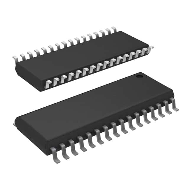
- Part No.:
- MCZ33781EKR2
- Manufacturer:
- NXP Semiconductors
- Category:
- Specialized
- Package:
- 32-SSOP (0.295", 7.50mm Width) Exposed Pad
- Datasheet:
-
 MCZ33781EKR2.pdf
- Description:
- IC INTERFACE SPECIALIZED 32SOIC
- Quantity:
- Payment:

- Shipping:

Inventory:3,212
Please send an inquiry. Send us your inquiry, and we will respond immediately.
Product details
Overview
MCZ33781EKR2 from NXP Semiconductors (formerly Freescale) is a quad-channel differential DSI 2.02 master IC for automotive and industrial distributed bus systems. It integrates four independent DBUS transceivers, dual SPI interfaces (SPI0 for command/control, SPI1 for response readout), on-chip 2.5 V digital regulator, and per-channel frequency spreading to reduce EMI. It drives up to four 2-wire differential buses carrying both power and data to remote slave modules in vehicle body electronics.
For engineers reviewing the MCZ33781EKR2 datasheet, MCZ33781EKR2 pinout, MCZ33781EKR2 application, or MCZ33781EKR2 equivalent, this device is selected for high-noise-robust, multi-slave DSI 2.02 master implementations requiring simultaneous bus control, CRC-protected messaging, and thermal/fault-aware bus driver operation across -40°C to +90°C ambient.
Technical Context
The MCZ33781EKR2 implements a full DSI 2.02 physical and protocol layer: each of its four channels generates differential voltage waveforms (DnH/DnL) with programmable slew rates (3–8 V/μs), supports 77.1–200 kbps data rate before frequency spreading, and embeds automatic CRC generation/checking per message. Its dual-SPI architecture separates command injection (SPI0) from asynchronous response retrieval (SPI1), enabling real-time monitoring of slave replies without interrupting master control flow.
Internally, it uses VSUP1 (9–25 V) to power DBUS0/DBUS1 and generate VCM_REF, while VSUP2 (9–25 V) supplies the charge pump for all four driver stages; both supplies are mandatory for full functionality. The pseudo-bus switch on Channel 0 (DPH/DPL) provides a second independent bus path using D0H/D0L resources under MCU control via SPI0.
Key Specifications
| Parameter | Value and Actual Design Meaning |
|---|---|
| Data Rate (pre-spread) | 77.1–200 kbps - defines maximum raw command throughput per DBUS channel |
| Bus Voltage Range (VSUPn) | 9.0–25 V - powers slave devices and sets differential swing via VMID = VSUPn/2 ±0.8 V |
| Differential Output Swing | 1.175–4.825 V (VDnD) - ensures robust signal margin against noise and cable loss |
| Slew Rate (Idle↔Signal) | 3.0–8.0 V/μs - balances EMI reduction with timing compliance for DSI 2.02 waveform shape |
| Operating Temperature | -40°C to +90°C - qualified for under-hood and body-control module environments |
| Logic Supply (VCC) | 4.75–5.25 V - powers digital core and SPI interfaces; internal 2.5 V regulator (VDD) derived from it |
| Thermal Shutdown Threshold | 155–190°C - protects bus drivers during sustained overcurrent or overload conditions |
Pinout & Package
MCZ33781EKR2 is housed in a 32-pin SOICW EP (exposed pad) package, Pb-free (EK suffix), with thermal resistance RθJA = 71°C/W and RθJB = 6°C/W. Pin layout supports dual-SPI isolation, separate analog/digital/power grounds, and dedicated high-current DBUS driver outputs with built-in current limiting and fault detection.
| Pin/Terminal | Circuit Role | Design Meaning |
|---|---|---|
| RST | Asynchronous Reset Input | Drives all registers to known state; active-low, requires ≥100 ns pulse width |
| SCLK0 / SCLK1 | SPI Clock Inputs | Separate clocks for SPI0 (command) and SPI1 (response); 100 ns min cycle time |
| MOSI0 / MISO0 / MISO1 | SPI Data Lines | MOSI0 accepts commands; MISO0 returns status/data; MISO1 delivers slave responses from Ch2/Ch3 |
| CS0 / CS1 | SPI Chip Selects | Enable SPI0 (Ch0/Ch1 control) and SPI1 (Ch2/Ch3 response readout) independently |
| D0H–D3H, D0L–D3L | Differential Bus Drivers | Four independent high-side/low-side outputs; each pair drives one DSI 2.02 bus with 400 mA max output |
| DPH / DPL | Pseudo-Bus Switch Outputs | Secondary bus path derived from Channel 0; controlled via SPI0 register, enables daisy-chain expansion |
| VSUP1 / VSUP2 | Positive Bus Supply Inputs | VSUP1 powers Ch0/Ch1 and VCM_REF; VSUP2 powers charge pump for all drivers; both required |
| VCC / VDD / AGND / VSS / GND | Power & Ground Terminals | Separate logic (VCC/VDD/VSS), analog (AGND), and bus power return (GND) paths prevent noise coupling |
Key Features
| Feature | Design Value |
|---|---|
| Quad Independent DSI 2.02 Channels | Enables concurrent control of four physically isolated bus segments-ideal for zone-based vehicle architectures |
| Dual SPI Interface Architecture | SPI0 handles full register access and command queuing; SPI1 provides non-blocking readout of slave responses from Ch2/Ch3 |
| Per-Channel Frequency Spreading | Reduces peak EMI by ±2% spectral spreading at base frequencies 77.1–200 kHz-critical for EMC-compliant designs |
| Automatic CRC Generation/Checking | Hardware-accelerated 0–8 bit CRC per message eliminates MCU overhead and guarantees data integrity end-to-end |
| Pseudo-Bus Switch on Channel 0 | Reuses D0H/D0L resources to create a second independent bus (DPH/DPL), doubling node capacity without extra ICs |
| Enhanced Fault Tolerance | Includes VSUP undervoltage lockout with mask time, thermal shutdown (155–190°C), and per-channel overcurrent shutdown (20–60 mA) |
Applications
| Body Control Module (BCM) | Seat Control Unit |
|---|---|
Use Scenario: Centralized management of door locks, window lifts, mirrors, and interior lighting via daisy-chained slave nodes. IC Role / Device Role / Timing Role: DSI 2.02 master coordinating up to four independent bus segments-one per vehicle quadrant-with CRC-protected command broadcast. Use Value: Reduces wiring harness weight and cost by replacing CAN/LIN with single twisted-pair per zone while maintaining functional safety via hardware CRC and fault reporting. |
Use Scenario: Real-time actuation of seat position motors, heating elements, and memory presets using distributed slave sensors and drivers. IC Role / Device Role / Timing Role: Master controller delivering synchronized position commands and reading back current/torque feedback over differential DBUS links. Use Value: Immunity to cabin EMI ensures reliable motor control during RF transmission or ignition events; frequency spreading meets CISPR 25 Class 3 limits. |
| Roof Module (Sunroof/Blinds) | Trunk/Liftgate Actuation |
Use Scenario: Coordinating sunroof glass movement, shade deployment, and rain sensor integration across multiple mechanical subsystems. IC Role / Device Role / Timing Role: DSI 2.02 master managing two dedicated buses-one for motor drivers, one for sensors-using pseudo-bus expansion on Channel 0. Use Value: Pseudo-bus capability allows dual-path communication over same physical wires, eliminating need for additional bus drivers or connectors. |
Use Scenario: Controlling liftgate latch release, strut assist, and anti-pinch sensing in premium rear cargo systems. IC Role / Device Role / Timing Role: High-reliability master enforcing strict timing (tBIT = 5.0 μs min) and fault response (<7 μs overcurrent shutdown) for safety-critical motion control. Use Value: Integrated thermal shutdown and VSUP monitoring prevent latch seizure or uncontrolled motion during voltage sag or overheating. |
Equivalent & Alternatives
The following parts are listed as comparable options for similar DSI master applications.
| Alternative Part | Technical Difference | Application Difference | Selection Advice |
|---|---|---|---|
| MC33880AEKR2 | Single-channel DSI 2.02 master; no frequency spreading; SPI0 only; no pseudo-bus | Lower channel count and no EMI reduction features limit use to simpler, lower-node-count systems | Select when only one bus segment is needed and cost sensitivity outweighs EMI requirements |
| MC33782EKR2 | Quad-channel like MCZ33781EKR2 but lacks SPI1 interface and pseudo-bus switch; identical DSI timing and driver specs | Cannot support concurrent command + response handling for Ch2/Ch3; reduces system-level latency visibility | Choose where response polling via SPI0 suffices and dual-SPI architecture adds unnecessary complexity |
Compared with MC33780AEKR2 and MC33782EKR2, the MCZ33781EKR2 uniquely delivers quad-channel operation with dual-SPI separation and pseudo-bus expansion-enabling scalable, low-EMI, high-diagnostic-capability DSI 2.02 networks for modern vehicle domains.
Availability
MCZ33781EKR2 is available at Aetrix Electronics and suitable for automotive body electronics, seat control units, roof modules, and liftgate actuation systems requiring stable component supply, long lifecycle support, and AEC-Q100-compliant performance.
Supply support for MCZ33781EKR2 includes scheduled delivery planning, volume procurement assistance, BOM continuity management, traceable sourcing, and lifecycle availability coordination for OEM customers, industrial embedded developers, connected-device designers, and electronics production programs.
Manufacturer
NXP Semiconductors is a global semiconductor leader focused on secure connectivity solutions for automotive, industrial, and IoT applications, with deep expertise in automotive-grade analog and mixed-signal ICs.
The MCZ33781EKR2 belongs to NXP's DSI 2.02 master product line, engineered specifically for high-reliability, EMI-resilient distributed bus architectures in vehicle body electronics where power-over-bus and deterministic timing are critical.
FAQ
What is the primary function of the MCZ33781EKR2 in a vehicle network?
The MCZ33781EKR2 serves as a quad-channel differential DSI 2.02 master IC that controls up to four independent 2-wire buses, delivering both power and data to remote slave devices in automotive body electronics. It executes protocol generation, CRC validation, frequency spreading, and bus driver control-all integrated into a single 32-pin SOICW EP package. Its dual-SPI architecture and pseudo-bus switch make the MCZ33781EKR2 especially suited for scalable, fault-aware vehicle domain controllers.
Does the MCZ33781EKR2 require both VSUP1 and VSUP2 supplies to operate?
Yes, the MCZ33781EKR2 requires both VSUP1 and VSUP2 supplies to be present and within 9.0–25 V for full functionality. VSUP1 powers DBUS Channels 0 and 1 and generates the VCM_REF reference voltage used by all four driver buffers. VSUP2 supplies the internal charge pump that drives the NMOS output stages of all bus drivers. Omitting either supply will result in partial or complete failure of bus output operation, as confirmed in the VSUP Block Diagram (Figure 9) and Functional Descriptions section.
How does the pseudo-bus feature of the MCZ33781EKR2 work?
The pseudo-bus feature of the MCZ33781EKR2 uses internal switches to route Channel 0's D0H and D0L signals to dedicated DPH and DPL pins, creating a second independent bus path. This switch is controlled exclusively via SPI0 register writes-no external hardware is needed. It enables daisy-chained topologies or redundant communication paths on the same physical wiring, effectively doubling node capacity on Channel 0 without adding another master IC. The MCZ33781EKR2 datasheet specifies matching resistance (≤1.0 Ω) and leakage (<±20 μA) to ensure signal integrity.
What is the role of SPI1 in the MCZ33781EKR2 architecture?
SPI1 in the MCZ33781EKR2 is a dedicated read-only interface that allows a second microcontroller-or a secondary core-to retrieve valid response data from DBUS Channels 2 and 3 without interfering with the primary SPI0 command/control channel. It accesses eight read-only registers containing slave addresses and payload data, enabling true parallelism: SPI0 can issue new commands while SPI1 asynchronously reads prior responses. This architecture reduces system latency and simplifies software task partitioning in multi-MCU vehicle ECUs using the MCZ33781EKR2.
Is the MCZ33781EKR2 compliant with AEC-Q100 for automotive use?
Yes, the MCZ33781EKR2 is qualified to AEC-Q100 Grade 2 (-40°C to +105°C junction), with operating ambient temperature specified from -40°C to +90°C and junction temperature rated to +150°C. Its design includes thermal shutdown (155–190°C), VSUP undervoltage detection with mask time, and robust ESD protection (±2000 V HBM), all verified per AEC-Q100 stress test requirements. The Pb-free (EK) packaging and SOICW EP construction further support automotive manufacturing and reliability standards.
MCZ33781EKR2 Specifications
- Product attributes
- Attribute value
- Manufacturer:
- NXP Semiconductors
- Series:
- -
- Package/Case:
- 32-SSOP (0.295", 7.50mm Width) Exposed Pad
- Packaging:
- Tape & Reel (TR)
- Product Status:
- Active
- Applications:
- -
- Interface:
- SPI Serial
- Voltage - Supply:
- 4.75V ~ 5.25V
- Supplier Device Package:
- 32-SOIC-EP
- Grade:
- Automotive
- Qualification:
- -
- Mounting Type:
- Surface Mount
MCZ33781EKR2 FAQ
1.How can I place an order for MCZ33781EKR2 through Aetrix?
Please submit a Request for Quotation (RFQ) for MCZ33781EKR2 on Aetrix. Our sales agent will provide a competitive quotation and guide you through the order confirmation once you accept the terms.
2.Are the price and stock information for MCZ33781EKR2 reliable?
The price and inventory of MCZ33781EKR2 are updated periodically and may fluctuate due to market conditions. Stock and pricing data are typically refreshed every 24 hours. Quotation validity for MCZ33781EKR2 is usually 5 days.
3.What payment methods are accepted for MCZ33781EKR2?
We accept Wire Transfer, PayPal, Credit Card, Western Union, MoneyGram, and Escrow for MCZ33781EKR2 transactions.
Note: Certain payment methods may incur a processing fee.
4.How is shipping managed for MCZ33781EKR2?
MCZ33781EKR2 orders can be shipped via leading logistics carriers, including DHL, UPS, FedEx, TNT, or Registered Mail.
Once your MCZ33781EKR2 order is processed, you will receive an email with the shipment details and tracking number.
Note: Tracking information may take up to 24 hours to appear. Express delivery typically takes 3–5 business days.
5.How can I obtain technical support or documentation for MCZ33781EKR2?
For technical support, including MCZ33781EKR2 datasheets, pinout diagrams, or application guidance, please contact our engineering support team. They can provide detailed documentation and assistance for your MCZ33781EKR2 requirements.
6.How does Aetrix verify that MCZ33781EKR2 is sourced from the original manufacturer or authorized distributors?
All MCZ33781EKR2 products on Aetrix are procured from qualified distributors and authorized channels. Our dedicated quality assurance team conducts strict verification, including traceability checks and, if necessary, third-party testing. This ensures that MCZ33781EKR2 meets industry standards.
7.What is the process for return or replacement of MCZ33781EKR2?
All MCZ33781EKR2 units undergo pre-shipment inspection (PSI). If there is an issue with MCZ33781EKR2, returns or replacements are accepted under the following conditions:
1.Quantity discrepancies, incorrect items, or visible external defects (such as breakage or corrosion), acknowledged by Aetrix.
2.The issue is reported within 90 days of delivery.
3.The MCZ33781EKR2 part is unused and in its original packaging.
Return procedure for MCZ33781EKR2:
1.Submit a request within 90 days.
2.Obtain a Return Material Authorization (RMA) from Aetrix.
MCZ33781EKR2 Tags

-
NVT4857UKAZ
NXP Semiconductors

-
TCA8418RTWR
Texas Instruments

-
PCA9546APWR
Texas Instruments

-
MD0100N8-G
Microchip Technology

-
PCA9548APW,118
NXP Semiconductors

-
PCA9540BDP,118
NXP Semiconductors

-
PCA9548APWR
Texas Instruments

-
PCA9546APW,118
NXP Semiconductors

-
PTN3360DBS,518
NXP Semiconductors

-
PCA9546ABS,118
NXP Semiconductors

-
PCA9518PWR
Texas Instruments

-
PCA9545APW,118
NXP Semiconductors
Tech Hub

A practical engineering guide to 3.3V and 5V logic compatibility, input thresholds, resistor dividers, translator ICs, MOSFET level shifting, I2C pull-ups, timing limits and power-sequencing risks.

The 74HC595 uses push-pull logic outputs, while the TPIC6B595 uses 50 V open-drain DMOS sinks for higher-power loads. This guide compares timing, current limits, 3.3 V interfacing, load wiring, thermal…

The 74HC595 converts serial data into eight stable parallel outputs. This guide covers pin functions, shift and storage timing, OE and MR behavior, drive-current limits, cascading, voltage compatibilit…

A technical comparison of level-sensitive latches and edge-triggered flip-flops, covering timing windows, setup and hold limits, master–slave operation, time borrowing, race-through, HDL inference and…

A D latch stores one bit while Enable controls when data can pass. This reference covers gate-level operation, truth tables, transparency, setup and hold timing, LE versus OE, common ICs and practical …

An SR latch stores one bit through cross-coupled feedback. This engineering reference covers NOR and NAND implementations, truth tables, forbidden-state recovery, gated operation, switch debouncing, fa…

Latch circuits retain one bit through feedback. This technical reference covers SR and D latches, truth tables, transparency, timing limits, latch-versus-flip-flop behavior, applications and common log…

An engineering guide to LED driver operation, constant-current and constant-voltage outputs, linear and switching topologies, dimming, IC selection, calculations, replacement compatibility, and fault c…

Operational amplifier guide covering op amp basics, feedback, ideal vs real op amps, common configurations, buffer circuits, offset, bias current, gain-bandwidth, slew rate, rail-to-rail limits and sel…

Jumper cables guide covering safe connection order, red and black clamp placement, final ground connection, cable gauge, length, clamp quality, copper vs CCA cables, jump starter comparison and battery…


