
 My Inquiry
 My Account


NXP Semiconductors MCZ33884EG
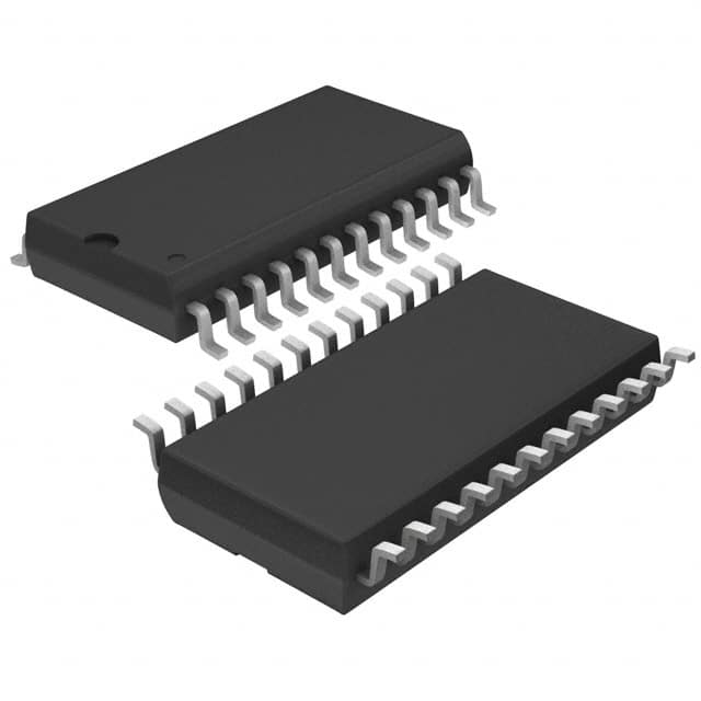
- Part No.:
- MCZ33884EG
- Manufacturer:
- NXP Semiconductors
- Category:
- Specialized
- Package:
- 24-SOIC (0.295", 7.50mm Width)
- Datasheet:
-
 MCZ33884EG.pdf
- Description:
- IC INTERFACE SPECIALIZED 24SOIC
- Quantity:
- Payment:

- Shipping:

Inventory:4,316
Please send an inquiry. Send us your inquiry, and we will respond immediately.
Product details
Overview
MCZ33884EG from NXP (formerly Freescale) is a monolithic switch monitor interface IC designed to interface electrical switches with low-voltage microprocessors in automotive and industrial control systems. It provides six switch-to-ground inputs, two switch-to-battery inputs, four programmable switch inputs, SPI-based configuration, and supports Sleep/Normal/Polling/Polling+INT Timer modes with <10 µA quiescent current in Sleep mode.
For engineers reviewing the MCZ33884EG datasheet, MCZ33884EG pinout, MCZ33884EG application, or MCZ33884EG equivalent, this page delivers verified technical context, real-world timing behavior, confirmed wetting/sustain current values, SPI command structure, and validated alternative options for switch monitoring system design.
Technical Context
The MCZ33884EG implements a configurable 16-bit SPI slave interface with MSB-first full-duplex protocol, supporting up to 3.5 MHz clock rate at 160 pF load. Its internal architecture includes six fixed-function switch-to-ground sense blocks, two fixed switch-to-battery blocks, and four programmable input blocks that support metallic/non-metallic detection via tri-state enable and wetting current control.
Each input uses a 4.0 V internal comparator reference: for SG pins, voltages <4.0 V indicate CLOSED; for SB/SP pins configured as switch-to-battery, >4.0 V indicates CLOSED. Wetting current pulses (–25 mA to +25 mA) activate for 34 ms typical upon closure, then decay to sustain levels (±0.75 mA), reducing power dissipation while maintaining contact integrity.
Key Specifications
| Parameter | Value and Actual Design Meaning |
|---|---|
| Supply Voltage Range | 7.0–26 V fully operational; 5.5–7.0 V quasi-functional (SPI active but fault reporting limited) |
| Input Voltage Range | –14 V to +40 V - enables direct connection to automotive battery rails with transient tolerance |
| Quiescent Current (Sleep) | <10 µA - ensures ultra-low standby power for always-on vehicle modules |
| Wetting Current (GND/BATT) | ±14 mA typical - reliably breaks oxide films on mechanical contacts without excessive heating |
| SPI Clock Frequency | 3.5 MHz max at 160 pF - supports fast status polling in real-time control loops |
| Switch Detection Threshold | 3.75 V typical (±0.5 V) - robust against noise while distinguishing open/closed states under varying loads |
| Interrupt Delay Time | 2.5–13 ms - defines worst-case latency between switch closure and MCU notification |
Pinout & Package
MCZ33884EG is housed in a 24-pin SOICW (wide-body) package with Pb-free EG suffix, rated for –40°C to +105°C operation. Pin spacing is 1.27 mm, body width 7.5 mm, and thermal resistance θJ-A = 107°C/W.
| Pin/Terminal | Circuit Role | Design Meaning |
|---|---|---|
| 1 VDD | 5.0 V logic supply | Provides regulated power to digital core and SPI interface; decoupling required near pin |
| 2 SO | SPI serial output | Tri-state open-drain output delivering 16-bit status word (MSB first); enabled only when CS is low |
| 3 SI | SPI serial input | Latches command bits on rising SCLK edge; internal pull-down ensures defined state when unconnected |
| 4 SP1 | Programmable switch input | Configurable as switch-to-ground or switch-to-battery; supports wetting/sustain current programming |
| 5–10 SG1–SG6 | Fixed switch-to-ground inputs | Dedicated sensing of grounded switches; closed = voltage <4.0 V; no configuration needed |
| 8,17 SB1, SB2 | Fixed switch-to-battery inputs | Dedicated sensing of battery-referenced switches; closed = voltage >4.0 V; no configuration needed |
| 11 VPWR | Main power supply | Derives all wetting/sustain currents; requires external reverse-battery and transient protection |
| 12 VSS | Ground reference | Common return for analog and digital sections; must be low-impedance path to minimize noise coupling |
| 13 RST | Active-low reset | Forces Sleep mode and clears registers; can be driven by MCU GPIO or system reset signal |
| 14 SYNC | Slave synchronization | Enables coordinated polling across multiple MCZ33884EG devices in master/slave topology |
| 15 INT | Open-drain interrupt output | Asserts on switch state change (Normal mode) or timeout (Polling+INT mode); requires external pull-up |
| 16–21 SP2–SP4, MASL, CS, SCLK | Control & interface signals | MASL selects master/slave role; CS enables SPI communication; SCLK clocks 16-bit shift register |
| 22 VBG | Bandgap reference output | 1.26 V typical; used with 130 kΩ resistor to set wetting/sustain current scaling |
| 23 CS | Chip select | Falling edge latches INT flag and switch status; rising edge disables SO and activates command |
| 24 SCLK | SPI clock input | Clocks SI data in and SO data out; must remain low during CS transitions to prevent spurious reads |
Key Features
| Feature | Design Value |
|---|---|
| Four configurable operating modes | Sleep (≤10 µA), Normal (real-time monitoring), Polling (reduced current), Polling+INT Timer (timeout-triggered wake-up) |
| Twelve dedicated switch sense inputs | Six SG-only, two SB-only, four SP-programmable - eliminates need for external conditioning circuitry |
| Programmable wetting current | ±7.5–25 mA per input - ensures reliable contact closure detection across diverse switch types and aging conditions |
| SPI-based configuration and status readback | 16-bit command/status words with MSB-first protocol - enables deterministic, noise-immune communication in EMI-heavy environments |
| Integrated ESD protection | 4 kV HBM on all pins - meets automotive requirements without additional TVS components on sense lines |
| Wide VPWR operating range | 5.5–26 V - supports 6 V, 12 V, and 24 V vehicle architectures with single BOM item |
Applications
| Automotive Body Control Module | Industrial Safety Interlock System |
|---|---|
|
Use Scenario: Monitoring door, hood, trunk, and seatbelt switches in a vehicle body controller. IC Role / Device Role / Timing Role: Centralized switch status acquisition unit with SPI interface to main MCU; handles wetting current sequencing and interrupt-driven state change reporting. Use Value: Reduces component count by integrating 12 switch inputs with programmable current drivers and fault-tolerant SPI communication - eliminating discrete transistors, resistors, and protection diodes per channel. |
Use Scenario: Verifying physical gate, guard door, and emergency stop button positions in factory automation machinery. IC Role / Device Role / Timing Role: Fail-safe switch monitor providing closed-loop verification of safety-critical mechanical actuations before enabling motion sequences. Use Value: Enables certified SIL-2 compliance through deterministic 13 ms max interrupt delay, dual threshold validation, and Sleep-mode current isolation during idle periods. |
| Aerospace Cabin Environmental Control | Robotic End-Effector Status Monitoring |
|
Use Scenario: Detecting position of air vent flaps, cabin light switches, and oxygen mask deployment latches in commercial aircraft. IC Role / Device Role / Timing Role: High-reliability switch interface with extended temperature range (–40°C to +105°C) and transient-hardened inputs for avionics-grade monitoring. Use Value: Meets DO-160 Section 22 lightning-induced transient requirements via built-in –14 V to +40 V input tolerance and integrated ESD protection - reducing board-level filtering complexity. |
Use Scenario: Reading tactile, limit, and tool-change confirmation switches on robotic grippers and end-of-arm tooling. IC Role / Device Role / Timing Role: Real-time switch status aggregator with programmable wetting current to overcome contact resistance drift caused by lubricants or particulate buildup. Use Value: Maintains >99.9% detection reliability over 10M cycles by dynamically applying 14 mA wetting pulse on closure, then stepping down to 0.75 mA sustain - minimizing self-heating and oxidation. |
Equivalent & Alternatives
The following parts are listed as comparable options for similar switch monitoring applications.
| Alternative Part | Technical Difference | Application Difference | Selection Advice |
|---|---|---|---|
| NCV33884DR2G | Pb-free SOICW package, identical pinout and SPI command set; specified for automotive AEC-Q100 Grade 1 (–40°C to +125°C) | Supports higher ambient temperature in engine bay or under-hood ECUs where +105°C is insufficient | Select NCV33884DR2G when operating junction temperature exceeds 105°C or AEC-Q100 qualification is mandatory. |
| MAX14912ATP+ | Octal high-side switch monitor with integrated 250 mA drivers; SPI interface but no wetting current control or sleep mode | Replaces discrete driver + sense circuits but lacks low-power polling modes and multi-threshold detection | Choose MAX14912ATP+ only when driving solenoids/valves is required alongside monitoring - not a drop-in replacement for pure switch sensing. |
Compared with MCZ33884EG, NCV33884DR2G extends temperature capability without changing layout or firmware, while MAX14912ATP+ trades ultra-low sleep current and flexible input configuration for integrated drive strength - making it suitable for actuator feedback but not for high-channel-count, low-power monitoring.
Availability
MCZ33884EG is available at Aetrix Electronics and suitable for automotive body control modules, industrial safety interlock systems, and aerospace cabin environmental controls requiring stable component supply across extended temperature ranges and long production lifecycles.
Supply support for MCZ33884EG includes scheduled delivery planning, volume procurement assistance, BOM continuity management, traceable sourcing, and lifecycle availability coordination for OEM customers, industrial embedded developers, connected-device designers, and electronics production programs.
Manufacturer
NXP Semiconductors is a global semiconductor leader focused on secure connectivity solutions for automotive, industrial, and IoT applications, with deep heritage in automotive analog and mixed-signal ICs.
The MCZ33884EG belongs to NXP's legacy Freescale analog switch monitor product line, engineered specifically for robust, low-power, multi-input switch status acquisition in harsh automotive and industrial environments.
FAQ
What is the maximum VPWR voltage the MCZ33884EG can withstand?
The MCZ33884EG supports a maximum VPWR voltage of 50 V under absolute maximum ratings, though continuous operation is specified from 7.0 V to 26 V. Transient spikes up to 40 V on switch inputs are tolerated when appropriate ESD capacitors are used. For sustained operation above 26 V, external clamping is required to avoid exceeding the 50 V limit and ensure long-term reliability of the device.
Does the MCZ33884EG support both switch-to-ground and switch-to-battery configurations on the same pin?
No - the MCZ33884EG assigns fixed roles: SG1–SG6 pins are switch-to-ground only, SB1–SB2 are switch-to-battery only, and SP1–SP4 are programmable for either configuration via SPI command. Each SP pin's behavior is determined by its CP[4:1] bitfield in the Run command; once configured, it remains fixed until reprogrammed. There is no hardware auto-detection or dynamic switching between modes per pin.
How does the MCZ33884EG handle switch debouncing?
The MCZ33884EG does not implement internal hardware debouncing. Instead, it relies on the microprocessor to apply software-based filtering using the reported switch status and interrupt timing. The device guarantees a minimum 2.5 ms interrupt delay (tINT(DELAY)), which provides a natural lower bound for debounce window design. Firmware must sample status over multiple SPI reads spaced ≥10 ms apart to reject mechanical bounce artifacts.
Can multiple MCZ33884EG devices share a single SPI bus?
Yes - multiple MCZ33884EG devices can operate on one SPI bus using individual chip select (CS) lines. In parallel configuration, each device responds only when its CS is asserted low. For daisy-chained serial configuration, 32 clock cycles are required per transfer, and the SO of one device connects to the SI of the next. The MASL and SYNC pins coordinate polling synchronization in multi-device systems to minimize total system current draw.
What is the purpose of the VBG pin on the MCZ33884EG?
The VBG pin outputs a 1.26 V bandgap reference voltage used to set wetting and sustain current magnitudes. A 130 kΩ resistor connected from VBG to ground establishes the reference current that scales all programmed current values. This external resistor allows precise calibration of input currents without trimming internal circuitry - ensuring consistent performance across temperature and process variations in production units of MCZ33884EG.
MCZ33884EG Specifications
- Product attributes
- Attribute value
- Manufacturer:
- NXP Semiconductors
- Series:
- -
- Package/Case:
- 24-SOIC (0.295", 7.50mm Width)
- Packaging:
- Tube
- Product Status:
- Obsolete
- Applications:
- Switch Monitoring
- Interface:
- SPI
- Voltage - Supply:
- 7V ~ 26V
- Supplier Device Package:
- 24-SOIC
- Grade:
- -
- Qualification:
- -
- Mounting Type:
- Surface Mount
MCZ33884EG FAQ
1.How can I place an order for MCZ33884EG through Aetrix?
Please submit a Request for Quotation (RFQ) for MCZ33884EG on Aetrix. Our sales agent will provide a competitive quotation and guide you through the order confirmation once you accept the terms.
2.Are the price and stock information for MCZ33884EG reliable?
The price and inventory of MCZ33884EG are updated periodically and may fluctuate due to market conditions. Stock and pricing data are typically refreshed every 24 hours. Quotation validity for MCZ33884EG is usually 5 days.
3.What payment methods are accepted for MCZ33884EG?
We accept Wire Transfer, PayPal, Credit Card, Western Union, MoneyGram, and Escrow for MCZ33884EG transactions.
Note: Certain payment methods may incur a processing fee.
4.How is shipping managed for MCZ33884EG?
MCZ33884EG orders can be shipped via leading logistics carriers, including DHL, UPS, FedEx, TNT, or Registered Mail.
Once your MCZ33884EG order is processed, you will receive an email with the shipment details and tracking number.
Note: Tracking information may take up to 24 hours to appear. Express delivery typically takes 3–5 business days.
5.How can I obtain technical support or documentation for MCZ33884EG?
For technical support, including MCZ33884EG datasheets, pinout diagrams, or application guidance, please contact our engineering support team. They can provide detailed documentation and assistance for your MCZ33884EG requirements.
6.How does Aetrix verify that MCZ33884EG is sourced from the original manufacturer or authorized distributors?
All MCZ33884EG products on Aetrix are procured from qualified distributors and authorized channels. Our dedicated quality assurance team conducts strict verification, including traceability checks and, if necessary, third-party testing. This ensures that MCZ33884EG meets industry standards.
7.What is the process for return or replacement of MCZ33884EG?
All MCZ33884EG units undergo pre-shipment inspection (PSI). If there is an issue with MCZ33884EG, returns or replacements are accepted under the following conditions:
1.Quantity discrepancies, incorrect items, or visible external defects (such as breakage or corrosion), acknowledged by Aetrix.
2.The issue is reported within 90 days of delivery.
3.The MCZ33884EG part is unused and in its original packaging.
Return procedure for MCZ33884EG:
1.Submit a request within 90 days.
2.Obtain a Return Material Authorization (RMA) from Aetrix.
MCZ33884EG Tags

-
NVT4857UKAZ
NXP Semiconductors

-
TCA8418RTWR
Texas Instruments

-
PCA9546APWR
Texas Instruments

-
MD0100N8-G
Microchip Technology

-
PCA9548APW,118
NXP Semiconductors

-
PCA9540BDP,118
NXP Semiconductors

-
PCA9548APWR
Texas Instruments

-
PCA9546APW,118
NXP Semiconductors

-
PTN3360DBS,518
NXP Semiconductors

-
PCA9546ABS,118
NXP Semiconductors

-
PCA9518PWR
Texas Instruments

-
PCA9545APW,118
NXP Semiconductors
Tech Hub

A practical engineering guide to 3.3V and 5V logic compatibility, input thresholds, resistor dividers, translator ICs, MOSFET level shifting, I2C pull-ups, timing limits and power-sequencing risks.

The 74HC595 uses push-pull logic outputs, while the TPIC6B595 uses 50 V open-drain DMOS sinks for higher-power loads. This guide compares timing, current limits, 3.3 V interfacing, load wiring, thermal…

The 74HC595 converts serial data into eight stable parallel outputs. This guide covers pin functions, shift and storage timing, OE and MR behavior, drive-current limits, cascading, voltage compatibilit…

A technical comparison of level-sensitive latches and edge-triggered flip-flops, covering timing windows, setup and hold limits, master–slave operation, time borrowing, race-through, HDL inference and…

A D latch stores one bit while Enable controls when data can pass. This reference covers gate-level operation, truth tables, transparency, setup and hold timing, LE versus OE, common ICs and practical …

An SR latch stores one bit through cross-coupled feedback. This engineering reference covers NOR and NAND implementations, truth tables, forbidden-state recovery, gated operation, switch debouncing, fa…

Latch circuits retain one bit through feedback. This technical reference covers SR and D latches, truth tables, transparency, timing limits, latch-versus-flip-flop behavior, applications and common log…

An engineering guide to LED driver operation, constant-current and constant-voltage outputs, linear and switching topologies, dimming, IC selection, calculations, replacement compatibility, and fault c…

Operational amplifier guide covering op amp basics, feedback, ideal vs real op amps, common configurations, buffer circuits, offset, bias current, gain-bandwidth, slew rate, rail-to-rail limits and sel…

Jumper cables guide covering safe connection order, red and black clamp placement, final ground connection, cable gauge, length, clamp quality, copper vs CCA cables, jump starter comparison and battery…


