
 My Inquiry
 My Account


NXP Semiconductors MIMX8MQ5CVAHZAB
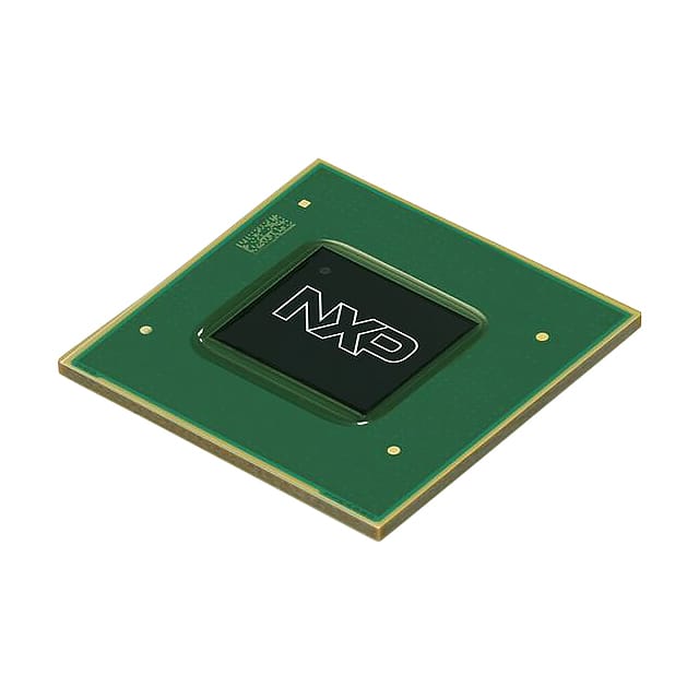
- Part No.:
- MIMX8MQ5CVAHZAB
- Manufacturer:
- NXP Semiconductors
- Category:
- Microprocessors
- Package:
- 621-FBGA, FCBGA
- Datasheet:
-
 MIMX8MQ5CVAHZAB.pdf
- Description:
- IC MPU I.MX8MQ 1.3GHZ 621FCPBGA
- Quantity:
- Payment:

- Shipping:

Inventory:1,440
Please send an inquiry. Send us your inquiry, and we will respond immediately.
Product details
Overview
MIMX8MQ5CVAHZAB from NXP Semiconductors is an industrial-grade i.MX 8M QuadLite applications processor featuring four Arm Cortex-A53 cores operating at 1.3 GHz, a dedicated Cortex-M4 core for low-power tasks, 1 MB L2 cache, LPDDR4-3200/DDR4-2400 memory support, and no integrated Video Processing Unit (VPU). It targets embedded multimedia gateways, industrial HMIs, and secure IoT edge controllers requiring high CPU throughput without hardware video decode.
For engineers reviewing the MIMX8MQ5CVAHZAB datasheet, MIMX8MQ5CVAHZAB pinout, MIMX8MQ5CVAHZAB application, or MIMX8MQ5CVAHZAB equivalent, key selection criteria include its quad-A53 + M4 architecture, absence of VPU acceleration, industrial temperature range (–40°C to +105°C), FBGA 17 × 17 mm package with 0.65 mm pitch, and support for HDMI 2.0a, MIPI-CSI2/DSI, dual USB 3.0/2.0, and Gigabit Ethernet with IEEE 1588.
Technical Context
The MIMX8MQ5CVAHZAB implements a symmetric quad-core Arm Cortex-A53 platform with full 64-bit Armv8-A compliance, including 32 KB L1 instruction and data caches per core and ECC-protected 1 MB unified L2 cache. Its Cortex-M4 core includes 16 KB I-cache, 16 KB D-cache, and 256 KB TCM for real-time firmware execution independent of the A53 cluster.
It integrates a comprehensive I/O subsystem: two PCIe Gen2 interfaces, dual USB 3.0/2.0 controllers with PHYs, four UARTs, four I²C modules, three SPI controllers, two uSDHC interfaces (one supporting 8-bit eMMC 5.0), and dual 4-lane MIPI-CSI2 camera inputs. Memory interface supports 32/16-bit LPDDR4-3200, DDR4-2400, and DDR3L-1600 with up to 8 GB addressable space.
Key Specifications
| Parameter | Value and Actual Design Meaning |
|---|---|
| CPU Architecture | Quad Arm Cortex-A53 @ 1.3 GHz + single Cortex-M4; enables Linux-based application processing with deterministic real-time control in parallel. |
| L2 Cache | 1 MB unified, ECC-protected; reduces memory bandwidth pressure and improves deterministic latency for multi-threaded workloads. |
| Memory Support | LPDDR4-3200 / DDR4-2400 / DDR3L-1600 (32/16-bit); allows flexible, cost-optimized memory subsystem design with industrial-grade reliability. |
| Temperature Range | –40°C to +105°C (Tj); qualified for continuous operation in harsh industrial environments without derating. |
| Package | FBGA, 17 × 17 mm, 0.65 mm pitch, bare die; compatible with standard PCB assembly processes and thermal management for high-power SoCs. |
| Security Features | Arm TrustZone, CAAM cryptographic accelerator (32 KB secure RAM), High Assurance Boot (HAB), RDC with 4 domains; enables secure boot, encrypted storage, and domain-isolated firmware execution. |
| Graphics | GPU with 4 shaders, OpenGL ES 3.1/Vulkan support, 267M triangles/sec; delivers smooth UI rendering and 1080p60 display output via HDMI 2.0a or MIPI-DSI. |
Pinout & Package
Package: FBGA, 17 × 17 mm, 0.65 mm pitch, bare die - designed for high-density industrial PCB layouts with controlled impedance routing and thermal vias to internal ground/power planes.
| Pin/Terminal | Circuit Role | Design Meaning |
|---|---|---|
| VDD_ARM | Core power supply | 1.0 V nominal (1.1 V overdrive); supplies Cortex-A53 cluster; requires tight regulation and local decoupling for DVFS stability. |
| VDD_SOC | System-on-chip power | 1.0 V nominal; powers interconnect, GIC, CCM, and peripheral logic; shared rail with GPU/VPU domains (though VPU is disabled in this variant). |
| NVCC_DRAM | DRAM I/O supply | 1.1 V for LPDDR4, 1.2 V for DDR4; sets signal voltage level for DRAM interface; must be sequenced after VDD_DRAM. |
| BOOT_MODE[1:0] | Boot configuration input | Pulled high/low at reset to select boot source (eMMC, SD, QSPI, NAND); determines initial firmware load path before ROM execution. |
| HDMI_TX_CLK | HDMI pixel clock output | Differential 100 Ω LVDS output; drives HDMI 2.0a timing up to 600 MHz for 4K@30 or 1080p@60 display resolution. |
| MIPI_CSI0_D0_P/N | MIPI CSI2 lane 0 differential pair | High-speed serial video input (up to 1.5 Gbps/lane); supports connection to 4-lane image sensors for machine vision or surveillance. |
Key Features
| Feature | Design Value |
|---|---|
| Quad Cortex-A53 + Cortex-M4 heterogenous compute | Enables concurrent Linux OS execution (A53) and real-time sensor fusion/firmware control (M4) without RTOS coexistence overhead. |
| No integrated Video Processing Unit (VPU) | Reduces silicon area, power consumption, and BOM cost where software-based video decode (e.g., FFmpeg on A53) suffices for HD content. |
| HDMI 2.0a with HDCP 1.4/2.2 support | Delivers secure 4K@30 or 1080p@60 video output to commercial displays; HDCP licensing required for activation per NXP documentation. |
| Dual 4-lane MIPI-CSI2 interfaces | Supports simultaneous input from two high-resolution image sensors (e.g., stereo vision or dual-camera HMI), each up to 1.5 Gbps/lane. |
| Cryptographic Acceleration (CAAM) | Hardware-accelerated AES-256, SHA-256, RSA, and RNG with FIPS 140-2 validated PRNG; offloads crypto from A53 cores for secure OTA updates. |
| Industrial qualification (–40°C to +105°C) | Guarantees full functionality and timing compliance across extended temperature range without thermal throttling or feature disablement. |
Applications
| Industrial HMI Gateway | Secure Edge IoT Controller |
|---|---|
Use Scenario: Programmable logic controller (PLC) with touchscreen interface, fieldbus connectivity (Modbus TCP, EtherNet/IP), and local data logging. IC Role / Device Role / Timing Role: Main application processor executing real-time Linux (PREEMPT_RT), managing display rendering, fieldbus protocol stacks, and secure firmware updates. Use Value: Quad-A53 provides headroom for multi-service execution; Cortex-M4 handles deterministic I/O scanning; industrial temp rating ensures uptime in factory-floor cabinets. |
Use Scenario: Smart building controller aggregating HVAC, lighting, and access control data, with TLS-secured cloud telemetry and local policy enforcement. IC Role / Device Role / Timing Role: Root-of-trust anchor running secure boot, CAAM-accelerated TLS handshake, and isolated M4 firmware for sensor polling and watchdog supervision. Use Value: Hardware-enforced TrustZone domains prevent cloud-agent compromise from affecting local control logic; SNVS RTC maintains time during power loss. |
| Medical Display Terminal | Video Conferencing Endpoint |
Use Scenario: DICOM viewer terminal with 1080p medical-grade display, USB peripherals (keyboard/mouse), and network-connected PACS archive retrieval. IC Role / Device Role / Timing Role: Primary SoC handling GUI framework (Qt/Wayland), JPEG/MPEG-2 decode via software libraries, and encrypted DICOM file transfer over TLS. Use Value: GPU renders crisp UI elements at 60 fps; absence of VPU simplifies certification path by eliminating hardware video pipeline validation requirements. |
Use Scenario: Compact conference room endpoint with dual 1080p cameras, microphone array, speaker output, and WebRTC-based video streaming. IC Role / Device Role / Timing Role: Central media processor performing audio echo cancellation (M4), video encoding (A53 + GPU-accelerated OpenCL filters), and network stack offload. Use Value: Dual MIPI-CSI2 inputs enable synchronized stereo capture; SAI modules support 32-bit/384 kHz audio processing for wideband voice clarity. |
Equivalent & Alternatives
The following parts are listed as comparable options for similar applications processor applications.
| Alternative Part | Technical Difference | Application Difference | Selection Advice |
|---|---|---|---|
| MIMX8MQ6CVAHZAB | Includes full VPU with 4Kp60 HEVC/H.265 decode and HDR10 support; identical CPU, GPU, and I/O subsystem. | Required for hardware-accelerated 4K video playback or transcoding; adds ~150 mW typical active power and higher BOM cost. | Select when video decode performance, power efficiency under sustained video load, or HDR display capability are mandatory. |
| MIMX8MD6CVAHZAB | Dual Cortex-A53 @ 1.3 GHz; same M4, GPU, security, and I/O features; lacks one A53 core and associated L2 cache. | Suitable for cost-sensitive, lower-throughput applications where dual-core Linux concurrency suffices (e.g., basic HMIs, gateway routers). | Select when CPU thread count and L2 cache bandwidth are non-critical, and BOM reduction outweighs future scalability needs. |
Compared with MIMX8MQ6CVAHZAB, MIMX8MQ5CVAHZAB trades VPU acceleration for lower power and cost while retaining identical CPU/GPU/security capabilities; compared with MIMX8MD6CVAHZAB, it delivers 2× CPU core count and 2× L2 cache for demanding multi-service edge workloads.
Availability
MIMX8MQ5CVAHZAB is available at Aetrix Electronics and suitable for industrial HMIs, secure edge IoT controllers, medical display terminals, and video conferencing endpoints requiring stable component supply across long product lifecycles.
Supply support for MIMX8MQ5CVAHZAB includes scheduled delivery planning, volume procurement assistance, BOM continuity management, traceable sourcing, and lifecycle availability coordination for OEM customers, industrial embedded developers, connected-device designers, and electronics production programs.
Manufacturer
NXP Semiconductors is a global semiconductor leader focused on secure connectivity solutions for automotive, industrial, and IoT markets, with deep expertise in Arm-based application processors and edge AI acceleration.
The i.MX 8M family-including MIMX8MQ5CVAHZAB-is designed specifically for intelligent edge devices requiring rich multimedia, real-time control, and robust security in industrial temperature environments.
FAQ
What is the primary functional distinction between MIMX8MQ5CVAHZAB and MIMX8MQ6CVAHZAB?
The MIMX8MQ5CVAHZAB omits the Video Processing Unit (VPU) present in MIMX8MQ6CVAHZAB. This means MIMX8MQ5CVAHZAB does not support hardware-accelerated video decoding (e.g., 4Kp60 HEVC/H.265) or encoding. All video processing must be performed in software on the Cortex-A53 cores. The CPU, GPU, memory interface, security, and I/O subsystems are otherwise identical between the two parts.
Does MIMX8MQ5CVAHZAB support HDMI 2.0a output, and what resolutions are achievable?
Yes, MIMX8MQ5CVAHZAB supports HDMI 2.0a output with HDCP 1.4/2.2 capability (license required). It can drive resolutions up to 4096 × 2160 at 30 Hz or 1920 × 1080 at 60 Hz. The GPU and display controller handle scaling and composition; however, since MIMX8MQ5CVAHZAB lacks a VPU, video decode must be handled in software prior to display output.
What is the role of the Cortex-M4 core in MIMX8MQ5CVAHZAB, and how is it isolated from the A53 cluster?
In MIMX8MQ5CVAHZAB, the Cortex-M4 core executes deterministic, low-latency firmware-such as sensor polling, motor control, or watchdog supervision-while the Cortex-A53 cluster runs Linux. Isolation is enforced via Arm TrustZone, Resource Domain Controller (RDC), and separate memory maps. The M4 has dedicated 256 KB TCM and cannot access A53 L2 cache or main DRAM without explicit secure world arbitration.
Can MIMX8MQ5CVAHZAB boot from eMMC 5.0, and what boot modes are supported?
Yes, MIMX8MQ5CVAHZAB supports boot from eMMC 5.0 via its uSDHC1 controller, which implements an 8-bit interface. Supported boot sources include eMMC, SD card, QSPI flash (with XIP), NAND flash, and USB device mode. Boot mode is selected using BOOT_MODE[1:0] pins at reset, and the internal boot ROM validates signature and loads the next-stage bootloader from the configured device.
What security features are implemented in hardware on MIMX8MQ5CVAHZAB?
MIMX8MQ5CVAHZAB includes Arm TrustZone, Cryptographic Acceleration and Assurance Module (CAAM) with AES-256/SHA-256/RSA engines and 32 KB secure RAM, High Assurance Boot (HAB) with signed image verification, Secure Non-Volatile Storage (SNVS) with tamper-resistant RTC, Resource Domain Controller (RDC) for memory/peripheral access partitioning, and Secure JTAG Controller (SJC) with eFUSE-configurable lock modes.
MIMX8MQ5CVAHZAB Specifications
- Product attributes
- Attribute value
- Manufacturer:
- NXP Semiconductors
- Package/Case:
- 621-FBGA, FCBGA
- Series:
- i.MX8MQ
- Packaging:
- Tray
- Product Status:
- Active
- Core Processor:
- ARM® Cortex®-A53
- Number of Cores/Bus Width:
- 4 Core, 64-Bit
- Speed:
- 1.3GHz
- Co-Processors/DSP:
- ARM® Cortex®-M4
- RAM Controllers:
- DDR3L, DDR4, LPDDR4
- Graphics Acceleration:
- Yes
- Display & Interface Controllers:
- eDP, HDMI, MIPI-CSI, MIPI-DSI
- Ethernet:
- GbE
- SATA:
- -
- USB:
- USB 3.0 (2)
- Voltage - I/O:
- -
- Operating Temperature:
- -40°C ~ 105°C (TJ)
- Grade:
- -
- Qualification:
- -
- Security Features:
- ARM TZ, CAAM, HAB, RDC, RTC, SJC, SNVS
- Mounting Type:
- Surface Mount
- Supplier Device Package:
- 621-FCPBGA (17x17)
- Additional Interfaces:
- EBI/EMI, I2C, PCIe, SPI, UART, uSDHC
MIMX8MQ5CVAHZAB FAQ
1.How can I place an order for MIMX8MQ5CVAHZAB through Aetrix?
Please submit a Request for Quotation (RFQ) for MIMX8MQ5CVAHZAB on Aetrix. Our sales agent will provide a competitive quotation and guide you through the order confirmation once you accept the terms.
2.Are the price and stock information for MIMX8MQ5CVAHZAB reliable?
The price and inventory of MIMX8MQ5CVAHZAB are updated periodically and may fluctuate due to market conditions. Stock and pricing data are typically refreshed every 24 hours. Quotation validity for MIMX8MQ5CVAHZAB is usually 5 days.
3.What payment methods are accepted for MIMX8MQ5CVAHZAB?
We accept Wire Transfer, PayPal, Credit Card, Western Union, MoneyGram, and Escrow for MIMX8MQ5CVAHZAB transactions.
Note: Certain payment methods may incur a processing fee.
4.How is shipping managed for MIMX8MQ5CVAHZAB?
MIMX8MQ5CVAHZAB orders can be shipped via leading logistics carriers, including DHL, UPS, FedEx, TNT, or Registered Mail.
Once your MIMX8MQ5CVAHZAB order is processed, you will receive an email with the shipment details and tracking number.
Note: Tracking information may take up to 24 hours to appear. Express delivery typically takes 3–5 business days.
5.How can I obtain technical support or documentation for MIMX8MQ5CVAHZAB?
For technical support, including MIMX8MQ5CVAHZAB datasheets, pinout diagrams, or application guidance, please contact our engineering support team. They can provide detailed documentation and assistance for your MIMX8MQ5CVAHZAB requirements.
6.How does Aetrix verify that MIMX8MQ5CVAHZAB is sourced from the original manufacturer or authorized distributors?
All MIMX8MQ5CVAHZAB products on Aetrix are procured from qualified distributors and authorized channels. Our dedicated quality assurance team conducts strict verification, including traceability checks and, if necessary, third-party testing. This ensures that MIMX8MQ5CVAHZAB meets industry standards.
7.What is the process for return or replacement of MIMX8MQ5CVAHZAB?
All MIMX8MQ5CVAHZAB units undergo pre-shipment inspection (PSI). If there is an issue with MIMX8MQ5CVAHZAB, returns or replacements are accepted under the following conditions:
1.Quantity discrepancies, incorrect items, or visible external defects (such as breakage or corrosion), acknowledged by Aetrix.
2.The issue is reported within 90 days of delivery.
3.The MIMX8MQ5CVAHZAB part is unused and in its original packaging.
Return procedure for MIMX8MQ5CVAHZAB:
1.Submit a request within 90 days.
2.Obtain a Return Material Authorization (RMA) from Aetrix.
MIMX8MQ5CVAHZAB Tags

-
AT91SAM9260B-CU-999
Microchip Technology
-
AT91SAM9G25-CU
Microchip Technology

-
ATSAMA5D27C-CU
Microchip Technology
-
AT91SAM9X35-CU
Microchip Technology
-
AT91SAM9X25-CU
Microchip Technology

-
MCIMX6Y2CVM08AB
NXP Semiconductors
.JPG)
-
AM3352BZCZ100
Texas Instruments
-
AT91SAM9260B-CU
Microchip Technology

-
AT91SAM9260B-QU
Microchip Technology

-
ATSAMA5D31A-CU
Microchip Technology
-
AT91SAM9G20B-CU-999
Microchip Technology
-
MCIMX6Y2CVM05AB
NXP Semiconductors
Tech Hub

A practical engineering guide to 3.3V and 5V logic compatibility, input thresholds, resistor dividers, translator ICs, MOSFET level shifting, I2C pull-ups, timing limits and power-sequencing risks.

The 74HC595 uses push-pull logic outputs, while the TPIC6B595 uses 50 V open-drain DMOS sinks for higher-power loads. This guide compares timing, current limits, 3.3 V interfacing, load wiring, thermal…

The 74HC595 converts serial data into eight stable parallel outputs. This guide covers pin functions, shift and storage timing, OE and MR behavior, drive-current limits, cascading, voltage compatibilit…

A technical comparison of level-sensitive latches and edge-triggered flip-flops, covering timing windows, setup and hold limits, master–slave operation, time borrowing, race-through, HDL inference and…

A D latch stores one bit while Enable controls when data can pass. This reference covers gate-level operation, truth tables, transparency, setup and hold timing, LE versus OE, common ICs and practical …

An SR latch stores one bit through cross-coupled feedback. This engineering reference covers NOR and NAND implementations, truth tables, forbidden-state recovery, gated operation, switch debouncing, fa…

Latch circuits retain one bit through feedback. This technical reference covers SR and D latches, truth tables, transparency, timing limits, latch-versus-flip-flop behavior, applications and common log…

An engineering guide to LED driver operation, constant-current and constant-voltage outputs, linear and switching topologies, dimming, IC selection, calculations, replacement compatibility, and fault c…

Operational amplifier guide covering op amp basics, feedback, ideal vs real op amps, common configurations, buffer circuits, offset, bias current, gain-bandwidth, slew rate, rail-to-rail limits and sel…

Jumper cables guide covering safe connection order, red and black clamp placement, final ground connection, cable gauge, length, clamp quality, copper vs CCA cables, jump starter comparison and battery…


