
 My Inquiry
 My Account


NXP Semiconductors MKW21D256VHA5R
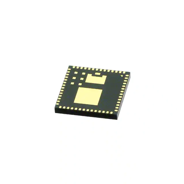
- Part No.:
- MKW21D256VHA5R
- Manufacturer:
- NXP Semiconductors
- Category:
- RF Transceiver ICs
- Package:
- 63-VFLGA
- Datasheet:
-
 MKW21D256VHA5R.pdf
- Description:
- IC RF TXRX+MCU 802.15.4 63MAPLGA
- Quantity:
- Payment:

- Shipping:

Inventory:1,818
Please send an inquiry. Send us your inquiry, and we will respond immediately.
Product details
Overview
MKW21D256VHA5R from NXP Semiconductors is a 50 MHz ARM Cortex-M4 MCU integrated with an IEEE 802.15.4-compliant 2.4 GHz radio transceiver, 256 KB flash, 32 KB SRAM, and FlexMemory (up to 64 KB FlexNVM + 4 KB FlexRAM), designed for ZigBee Home Automation and Thread edge nodes in smart energy gateways and in-home displays.
For engineers reviewing the MKW21D256VHA5R datasheet, MKW21D256VHA5R pinout, MKW21D256VHA5R application, or MKW21D256VHA5R equivalent, key selection criteria include –102 dBm receiver sensitivity, +8 dBm max TX power, 8×8 mm 56-pin LGA package, –40°C to 105°C operation, and absence of USB interface compared to MKW22D/MKW24D variants.
Technical Context
The MKW21D256VHA5R implements a near-zero-IF (NZIF) radio architecture with hardware-accelerated IEEE 802.15.4 packet processing, dual PAN ID support, and programmable output power from –35 dBm to +8 dBm across 16 ISM channels (2405–2480 MHz) and MBAN bands (2360–2400 MHz). It integrates a 32 MHz crystal oscillator with on-die trim and supports Low Power Preamble Search mode with 15 mA peak RX current.
Its MCU subsystem features DSP-capable Cortex-M4 core, cryptographic acceleration (AES/SHA/DES), 16-bit SAR ADC, 12-bit DAC, and 10 power modes-including hibernate with SPI access-enabling ultra-low-power wireless sensor node operation without external USB PHY.
Key Specifications
| Parameter | Value and Actual Design Meaning |
|---|---|
| CPU Core | ARM Cortex-M4 @ 50 MHz with DSP instructions - enables real-time MAC-layer processing and sensor fusion in battery-powered nodes. |
| Flash / SRAM | 256 KB flash + 32 KB SRAM + FlexMemory (64 KB FlexNVM / 4 KB FlexRAM) - supports over-the-air firmware updates and EEPROM-like wear-leveling without external memory. |
| Radio Sensitivity | –102 dBm @ 1% PER (20-byte packet) - ensures robust link budget in mesh networks with ≥58 dB channel rejection. |
| TX Output Power | +8 dBm max, programmable down to –35 dBm - allows precise RF range tuning and regulatory compliance across global 2.4 GHz bands. |
| Supply & Temp | 1.8 V–3.6 V operation, –40°C to 105°C ambient - qualified for industrial-grade metering and building control environments. |
| Package | 8 × 8 mm LGA, 56-pin - surface-mount compatible with high-density PCB layouts; no leaded package option. |
| USB Interface | Not integrated - distinguishes MKW21D256VHA5R from MKW22D/MKW24D; reduces BOM cost and layout complexity for headless endpoints. |
Pinout & Package
Packaged in an 8 × 8 mm, 56-contact LGA (Land Grid Array) with 0.5 mm pitch, optimized for RF integrity and thermal dissipation in compact wireless modules.
| Pin/Terminal | Circuit Role | Design Meaning |
|---|---|---|
| VDD_RF / VDD_ANA | Analog & RF supply | Dedicated 1.8–3.6 V rail decoupled separately to minimize noise coupling into sensitive RF receiver path. |
| RFOUTP / RFOUTN | Differential RF I/O | Bidirectional port supporting integrated T/R switch; requires external balun for single-ended antenna interface. |
| ANT_A / ANT_B | Antenna diversity control | GPIOs driving external antenna switches - enables automatic diversity selection without MCU intervention. |
| CLK_OUT (Pin 39) | Programmable clock output | 32 MHz reference divided down (32 MHz to 32.786 kHz); drives MCU EXTAL directly - eliminates need for separate system clock source. |
| R_SSEL_B / R_SCLK / R_MOSI / R_MISO | SPI slave interface | 4-wire SPI for register and 128-byte packet buffer access; supports burst reads/writes and hibernate-mode operation. |
| RESET_B | Active-low reset input | Asynchronous reset pin with internal pull-up; initiates full device initialization including radio and MCU subsystems. |
Key Features
| Feature | Design Value |
|---|---|
| Dual PAN ID hardware support | Simultaneous association to two IEEE 802.15.4 networks via independent PAN0/PAN1 registers, channel selection, and auto-switching timer - enables gateway bridging between HAN and WAN without software scheduling overhead. |
| Hardware packet processor | Fully offloads MAC-layer filtering (address matching, frame type, pending bit, promiscuous mode) - reduces MCU wake-ups and extends sleep duration in battery-operated end devices. |
| FlexMemory architecture | Configurable partitioning of up to 64 KB FlexNVM (emulated EEPROM) and 4 KB FlexRAM - enables field-upgradable parameter storage with 10M-cycle endurance across full voltage/temperature range. |
| Low-Power Preamble Search (LPPS) | 15 mA peak RX current during preamble detection with duty-cycled receiver sections - achieves >10-year battery life in periodic polling applications like thermostat sensors. |
| Cryptographic acceleration engine | Hardware AES-128/256, SHA-1/256, DES/3DES, and RNG - accelerates ZigBee SE, Thread, and Smart Energy 1.x security stack execution without CPU load. |
Applications
| Smart Energy Gateway | ZigBee Light Link Node |
|---|---|
Use Scenario: Residential electricity/gas/water meter data aggregation and secure forwarding to utility network via HAN/WAN bridge. IC Role / Device Role / Timing Role: Dual PAN coordinator managing IEEE 802.15.4 HAN (meters) and Thread/WAN (cloud uplink) simultaneously; uses CLK_OUT as precise 32 MHz timing reference for synchronized polling. Use Value: Eliminates external clock source and reduces bill-of-materials while maintaining <10 ppm frequency stability required for time-synchronized mesh routing. | Use Scenario: Wireless dimmable LED driver in retrofit lighting systems compliant with ZigBee Light Link v1.0. IC Role / Device Role / Timing Role: End-device node executing ZLL commissioning, group control, and scene recall; leverages hardware packet processor to filter broadcast commands and suppress redundant interrupts. Use Value: Achieves sub-100 ms command response with 32 KB SRAM holding ZLL profile stack and 256 KB flash storing certified ZLL firmware - no external memory needed. |
| Thread Border Router Endpoint | Home HVAC Sensor Hub |
Use Scenario: Low-cost, battery-powered Thread border router endpoint connecting BLE thermostats to IPv6 backbone. IC Role / Device Role / Timing Role: Thread 1.1.1-certified node performing 6LoWPAN header compression, mesh underlay routing, and secure key exchange using hardware crypto engine. Use Value: Hardware AES-256 and SHA-256 accelerate DTLS handshake by 4× vs. software-only, enabling secure join in <2 s - critical for installer UX. | Use Scenario: Multi-sensor hub monitoring temperature, humidity, and CO₂ in residential HVAC ducts with 10-year battery life. IC Role / Device Role / Timing Role: Ultra-low-power sensor concentrator using LPPS mode and 16-bit ADC to digitize analog sensor outputs; FlexRAM buffers readings during deep sleep. Use Value: 15 mA LPPS current + 1.8 V minimum operating voltage extends coin-cell lifetime beyond 10 years at 1-min sampling interval. |
Equivalent & Alternatives
The following parts are listed as comparable options for similar IEEE 802.15.4 wireless MCU applications.
| Alternative Part | Technical Difference | Application Difference | Selection Advice |
|---|---|---|---|
| MKW22D512VHA5R | Includes full-speed USB 2.0 interface and 512 KB flash/64 KB SRAM; no FlexMemory; same 8×8 LGA package. | Required for USB-based programming, debug, or host-attached dongle designs; not suitable for headless sensor nodes where USB adds cost and layout overhead. | Select MKW22D512VHA5R when USB device/host capability is mandatory and higher memory is needed; MKW21D256VHA5R remains optimal for cost-sensitive, USB-free endpoints. |
| EM3581-RTR | Legacy Ember ZigBee SoC (8051 core, 128 KB flash, –95 dBm sensitivity); QFN-48 package; no ARM Cortex-M4 or FlexMemory. | Limited to ZigBee PRO/HA stacks; lacks Thread/Smart Energy 2.0 support and modern crypto acceleration; lower RF performance. | EM3581-RTR suits legacy ZigBee HA redesigns with existing firmware; MKW21D256VHA5R provides future-proofing for Thread migration and enhanced security. |
Compared with MKW22D512VHA5R, MKW21D256VHA5R trades USB and extra memory for FlexMemory and lower BOM cost - ideal for firmware-upgradable sensor endpoints. Against EM3581-RTR, it delivers superior sensitivity (–102 vs –95 dBm), ARM-based toolchain continuity, and hardware crypto essential for Smart Energy 1.x certification.
Availability
MKW21D256VHA5R is available at Aetrix Electronics and suitable for smart energy gateways, ZigBee Light Link lighting controls, and Thread border router endpoints requiring stable component supply across extended product lifecycles.
Supply support for MKW21D256VHA5R includes scheduled delivery planning, volume procurement assistance, BOM continuity management, traceable sourcing, and lifecycle availability coordination for OEM customers, industrial embedded developers, connected-device designers, and electronics production programs.
Manufacturer
NXP Semiconductors is a global semiconductor leader specializing in secure connectivity solutions for automotive, industrial, and IoT applications, with headquarters in Eindhoven, Netherlands.
The MKW2xD family was engineered specifically for standards-based wireless mesh networking in resource-constrained, battery-powered edge devices - emphasizing low-power radio performance, integrated security, and seamless IEEE 802.15.4 protocol acceleration.
FAQ
What is the maximum transmit output power of the MKW21D256VHA5R?
The MKW21D256VHA5R supports a maximum transmit output power of +8 dBm, programmable in fine steps down to –35 dBm. This range enables precise RF link budget control for compliance with regional regulations (e.g., FCC Part 15.247, ETSI EN 300 328) and optimization of range versus battery life in ZigBee and Thread deployments.
Does the MKW21D256VHA5R include a USB interface?
No, the MKW21D256VHA5R does not integrate a USB interface. This distinguishes it from the MKW22D512VHA5R and MKW24D512VHA5R variants. The absence of USB reduces silicon area, BOM cost, and layout complexity - making MKW21D256VHA5R ideal for headless, battery-powered sensor nodes where serial or SWD debugging suffices.
What memory architecture does the MKW21D256VHA5R use, and how is it configured?
The MKW21D256VHA5R includes 256 KB of program flash, 32 KB of SRAM, and FlexMemory comprising up to 64 KB of FlexNVM and 4 KB of FlexRAM. FlexMemory is user-configurable via runtime commands to emulate EEPROM with 10 million write cycles, enabling robust parameter storage for Smart Energy 1.x and ZigBee SE applications without external nonvolatile memory.
What is the operating temperature range for the MKW21D256VHA5R?
The MKW21D256VHA5R is rated for an ambient operating temperature range of –40°C to +105°C. This industrial-grade specification ensures reliable operation in demanding environments such as smart meters mounted outdoors, HVAC control panels, and in-home displays exposed to wide thermal swings - validated per NXP's thermal handling and EMC radiated emissions requirements.
How does the MKW21D256VHA5R support dual PAN operation?
The MKW21D256VHA5R implements hardware-assisted dual PAN ID functionality with two independent sets of PAN parameters (PAN0/PAN1), including separate channels, PAN IDs, short/long addresses, and coordinator flags. A programmable timer enables automatic PAN switching without CPU involvement - allowing MKW21D256VHA5R to serve as a bridge between HAN and WAN networks in Smart Energy gateways while maintaining full protocol compliance on both sides.
MKW21D256VHA5R Specifications
- Product attributes
- Attribute value
- Manufacturer:
- NXP Semiconductors
- Series:
- -
- Package/Case:
- 63-VFLGA
- Packaging:
- Tape & Reel (TR)
- Product Status:
- Active
- Programmable:
- Not Verified
- Type:
- TxRx + MCU
- RF Family/Standard:
- 802.15.4
- Protocol:
- Zigbee®
- Modulation:
- DSSS, O-QPSK
- Frequency:
- 2.4GHz
- Data Rate (Max):
- 250kbps
- Power - Output:
- 8dBm
- Sensitivity:
- -102dBm
- Memory Size:
- 256kB Flash, 32kB SRAM
- Serial Interfaces:
- I2C, JTAG, SPI, UART
- GPIO:
- 2
- Voltage - Supply:
- 1.8V ~ 3.6V
- Current - Receiving:
- 15mA
- Current - Transmitting:
- 19mA
- Operating Temperature:
- -40°C ~ 105°C
- Grade:
- -
- Qualification:
- -
- Supplier Device Package:
- 63-MAPLGA (8x8)
MKW21D256VHA5R FAQ
1.How can I place an order for MKW21D256VHA5R through Aetrix?
Please submit a Request for Quotation (RFQ) for MKW21D256VHA5R on Aetrix. Our sales agent will provide a competitive quotation and guide you through the order confirmation once you accept the terms.
2.Are the price and stock information for MKW21D256VHA5R reliable?
The price and inventory of MKW21D256VHA5R are updated periodically and may fluctuate due to market conditions. Stock and pricing data are typically refreshed every 24 hours. Quotation validity for MKW21D256VHA5R is usually 5 days.
3.What payment methods are accepted for MKW21D256VHA5R?
We accept Wire Transfer, PayPal, Credit Card, Western Union, MoneyGram, and Escrow for MKW21D256VHA5R transactions.
Note: Certain payment methods may incur a processing fee.
4.How is shipping managed for MKW21D256VHA5R?
MKW21D256VHA5R orders can be shipped via leading logistics carriers, including DHL, UPS, FedEx, TNT, or Registered Mail.
Once your MKW21D256VHA5R order is processed, you will receive an email with the shipment details and tracking number.
Note: Tracking information may take up to 24 hours to appear. Express delivery typically takes 3–5 business days.
5.How can I obtain technical support or documentation for MKW21D256VHA5R?
For technical support, including MKW21D256VHA5R datasheets, pinout diagrams, or application guidance, please contact our engineering support team. They can provide detailed documentation and assistance for your MKW21D256VHA5R requirements.
6.How does Aetrix verify that MKW21D256VHA5R is sourced from the original manufacturer or authorized distributors?
All MKW21D256VHA5R products on Aetrix are procured from qualified distributors and authorized channels. Our dedicated quality assurance team conducts strict verification, including traceability checks and, if necessary, third-party testing. This ensures that MKW21D256VHA5R meets industry standards.
7.What is the process for return or replacement of MKW21D256VHA5R?
All MKW21D256VHA5R units undergo pre-shipment inspection (PSI). If there is an issue with MKW21D256VHA5R, returns or replacements are accepted under the following conditions:
1.Quantity discrepancies, incorrect items, or visible external defects (such as breakage or corrosion), acknowledged by Aetrix.
2.The issue is reported within 90 days of delivery.
3.The MKW21D256VHA5R part is unused and in its original packaging.
Return procedure for MKW21D256VHA5R:
1.Submit a request within 90 days.
2.Obtain a Return Material Authorization (RMA) from Aetrix.
MKW21D256VHA5R Tags

-
ESP32-D0WD-V3
Espressif Systems

-
ESP8266EX
Espressif Systems

-
ESP32-S3
Espressif Systems

-
NRF24L01P-R7
Nordic Semiconductor ASA
-
NRF24L01P-R
Nordic Semiconductor ASA

-
ESP32-U4WDH
Espressif Systems

-
DA14531-00000OG2
Renesas
-
ESP32-C6FH4
Espressif Systems

-
DA14531-00000FX2
Renesas
-
NRF24L01P-T
Nordic Semiconductor ASA

-
NRF52810-QCAA-R
Nordic Semiconductor ASA
-
ESP32-S3FN8
Espressif Systems
Tech Hub

A practical engineering guide to 3.3V and 5V logic compatibility, input thresholds, resistor dividers, translator ICs, MOSFET level shifting, I2C pull-ups, timing limits and power-sequencing risks.

The 74HC595 uses push-pull logic outputs, while the TPIC6B595 uses 50 V open-drain DMOS sinks for higher-power loads. This guide compares timing, current limits, 3.3 V interfacing, load wiring, thermal…

The 74HC595 converts serial data into eight stable parallel outputs. This guide covers pin functions, shift and storage timing, OE and MR behavior, drive-current limits, cascading, voltage compatibilit…

A technical comparison of level-sensitive latches and edge-triggered flip-flops, covering timing windows, setup and hold limits, master–slave operation, time borrowing, race-through, HDL inference and…

A D latch stores one bit while Enable controls when data can pass. This reference covers gate-level operation, truth tables, transparency, setup and hold timing, LE versus OE, common ICs and practical …

An SR latch stores one bit through cross-coupled feedback. This engineering reference covers NOR and NAND implementations, truth tables, forbidden-state recovery, gated operation, switch debouncing, fa…

Latch circuits retain one bit through feedback. This technical reference covers SR and D latches, truth tables, transparency, timing limits, latch-versus-flip-flop behavior, applications and common log…

An engineering guide to LED driver operation, constant-current and constant-voltage outputs, linear and switching topologies, dimming, IC selection, calculations, replacement compatibility, and fault c…

Operational amplifier guide covering op amp basics, feedback, ideal vs real op amps, common configurations, buffer circuits, offset, bias current, gain-bandwidth, slew rate, rail-to-rail limits and sel…

Jumper cables guide covering safe connection order, red and black clamp placement, final ground connection, cable gauge, length, clamp quality, copper vs CCA cables, jump starter comparison and battery…


