
 My Inquiry
 My Account


NXP Semiconductors MMPF0100F1EP
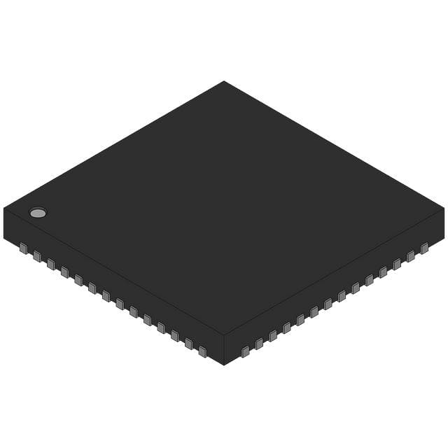
- Part No.:
- MMPF0100F1EP
- Manufacturer:
- NXP Semiconductors
- Category:
- Special Purpose Regulators
- Package:
- 56-VFQFN Exposed Pad
- Datasheet:
-
 MMPF0100F1EP.pdf
- Description:
- IC REG CONV I.MX6 12OUT 56HVQFN
- Quantity:
- Payment:

- Shipping:

Inventory:3,292
Please send an inquiry. Send us your inquiry, and we will respond immediately.
Product details
Overview
MMPF0100F1EP from NXP Semiconductors is a 14-channel configurable power management IC (PMIC) designed for i.MX 6SoloLite-based embedded platforms. It integrates six buck converters (including SW1A/B/C, SW2, SW3A/B, SW4), six linear regulators (VGEN1–VGEN6), coin-cell charger, RTC supply, DDR termination reference (VREFDDR), and I²C-controlled programmable sequencing - delivering full-system power for eReaders, medical monitors, and home automation devices.
For engineers reviewing the MMPF0100F1EP datasheet, MMPF0100F1EP pinout, MMPF0100F1EP application, or MMPF0100F1EP equivalent, key selection criteria include OTP-programmed F1 configuration for MCIMX6SLEVK reference design, 56-pin QFN 8×8 mm package with exposed thermal pad, -40 °C to +85 °C operating range, and support for DDR memory interface power integrity via VREFDDR tracking.
Technical Context
The MMPF0100F1EP implements a hierarchical power tree with independent control logic for each regulator group: core (VCORE/VCOREDIG), memory (VREFDDR, SW3A/B), and peripherals (VGEN1–VGEN6). Its OTP memory stores device-specific voltage setpoints, startup sequence timing, and enable/disable states - eliminating external configuration components.
It features dual-phase capability on SW1A/B and SW3A/B, DDR termination tracking mode, and integrated thermal monitoring with four interrupt thresholds (110°C–130°C). The I²C interface (SCL/SDA, 3.6 V tolerant) supports real-time register access for dynamic voltage scaling (DVS) and fault reporting without requiring processor reset.
Key Specifications
| Parameter | Value and Actual Design Meaning |
|---|---|
| Main input voltage | 2.8–4.5 V DC - powers all internal regulators; requires 4.7 μF + 0.1 μF local bypass at VIN |
| Buck output count | 6 channels (SW1A/B/C, SW2, SW3A/B, SW4) - supports up to 2.5 A per channel in industrial variants |
| LDO count & current | 6 general-purpose LDOs (VGEN1–VGEN6); outputs range 100–350 mA with fixed or programmable voltages |
| VREFDDR accuracy | ±1.5% over temperature - provides precise DDR memory termination reference tracking VDDQ/2 |
| I²C interface | Standard-mode (100 kHz) and fast-mode (400 kHz); 7-bit slave address 0x08; open-drain SDA/SCL |
| OTP memory | One-time programmable nonvolatile storage - holds boot configuration, voltage levels, sequencing order, and timing delays |
| Thermal protection | Four threshold interrupts (110°C/120°C/125°C/130°C); debounced 8 ms; shuts down regulators above 130°C |
Pinout & Package
Package: 56-pin QFN, 8 mm × 8 mm, 0.5 mm pitch, exposed thermal pad (EP). RoHS-compliant, wettable flank not applicable (E-Type suffix).
| Pin/Terminal | Circuit Role | Design Meaning |
|---|---|---|
| INTB (Pin 1) | Open-drain interrupt output | Signals fault conditions (thermal, overcurrent, POR) to host processor; pulled high externally |
| SW1ALX/SW1BLX (Pins 8–9) | Switch node outputs | Connect to external inductor for dual-phase SW1A/B operation; require low-inductance layout |
| VREFDDR (Pin 31) | DDR termination reference output | Provides precision 0.6–0.9 V reference for DDR memory termination resistors; routed with controlled impedance |
| VSNVS (Pin 43) | Always-on LDO/coin-cell output | Supplies real-time clock and backup domain; supports Li-cell charging via LICELL pin |
| EP (Exposed Pad) | Thermal & ground return | Must be soldered to inner/outer ground planes via ≥6 vias for thermal dissipation and noise reduction |
Key Features
| Feature | Design Value |
|---|---|
| Configurable buck topology | SW1A/B and SW3A/B support single/dual-phase or parallel operation - enables optimized efficiency vs. transient response trade-off |
| DDR termination tracking | VREFDDR dynamically tracks half of VDDQ rail - eliminates need for external resistor divider and improves DDR signal integrity |
| OTP-based boot configuration | F1-programmed variant preloads settings for MCIMX6SLEVK - reduces firmware initialization time and eliminates external EEPROM |
| Integrated coin-cell management | LICELL and VSNVS pins enable automatic charging and seamless switchover - sustains RTC during main power loss |
| Thermal event detection | Four independent interrupt thresholds with status register readback - allows graded system response (throttle → warn → shutdown) |
Applications
| eReader Power System | Medical Vital Signs Monitor |
|---|---|
Use Scenario: Low-power eInk display controller with i.MX 6SoloLite SoC, SD card, and touch interface requiring sequenced, low-noise power rails. IC Role / Device Role / Timing Role: MMPF0100F1EP delivers VCORE (1.2 V), VGEN2 (2.5 V for SDIO), VGEN4 (3.3 V for touch), and VREFDDR (0.75 V) with precise startup timing and DDR termination. Use Value: Eliminates discrete LDOs and sequencing ICs; OTP F1 config matches MCIMX6SLEVK BOM - reducing BOM count by 7 components. | Use Scenario: Portable patient monitor with ECG, SpO₂, and temperature sensors, requiring battery-backed RTC and ultra-low-quiescent LDOs. IC Role / Device Role / Timing Role: MMPF0100F1EP supplies VSNVS (always-on 1.8 V), VGEN1 (1.8 V for sensors), and VGEN5 (3.3 V for analog front-end) with <10 μA standby current. Use Value: Integrated coin-cell charger maintains RTC across 72-hour battery depletion; VGEN1/VGEN5 LDOs achieve ±1% load regulation at 100 mA. |
| Home Energy Gateway | Industrial PLC HMI Panel |
Use Scenario: Wi-Fi/Zigbee gateway with ARM Cortex-A9, flash memory, and isolated RS-485 interface operating in uncontrolled ambient environments. IC Role / Device Role / Timing Role: MMPF0100F1EP provides SW2 (2 A for SoC core), SW4 (1 A for Ethernet PHY), and VGEN6 (3.3 V for transceivers) with thermal throttling at 110°C. Use Value: On-die thermal sensing triggers early frequency scaling before junction exceeds 125°C - prevents unexpected resets in enclosed enclosures. | Use Scenario: Ruggedized HMI panel with LCD backlight, CAN bus, and microSD storage deployed in factory automation cabinets. IC Role / Device Role / Timing Role: MMPF0100F1EP powers VCOREDIG (1.5 V), SW3A/B (dual-phase 2.5 A for LCD driver), and VGEN3 (3.3 V for CAN transceiver) with robust ESD protection (±2 kV HBM). Use Value: Exposed pad (EP) and RθJB = 10°C/W enable reliable operation at 85°C ambient without heatsink - meeting IEC 61000-6-2 industrial immunity requirements. |
Equivalent & Alternatives
The following parts are listed as comparable options for similar PMIC applications.
| Alternative Part | Technical Difference | Application Difference | Selection Advice |
|---|---|---|---|
| MMPF0100F0AEP | F0 OTP config targets i.MX 6Quad/DualLite platforms; lacks SW2 2.5 A capability in consumer temp grade | Designed for MCIMX6Q-SDP; not validated for i.MX 6SoloLite voltage sequencing | Select only if migrating from Quad-based design; verify VGENx timing against F1's MCIMX6SLEVK profile |
| MMPF0100F3AEP | F3 OTP adds SW2 2.5 A support and extended VGEN2/VGEN4 voltage ranges; same package and pinout | Optimized for i.MX 6SoloLite EVK with higher peripheral current demands | Preferred for new designs needing >250 mA on VGEN2 or >350 mA on VGEN4; retains F1's core sequencing logic |
Compared with MMPF0100F0AEP and MMPF0100F3AEP, the MMPF0100F1EP offers the exact OTP configuration required for MCIMX6SLEVK - ensuring guaranteed startup behavior, correct DDR termination voltage, and minimal firmware adaptation effort.
Availability
MMPF0100F1EP is available at Aetrix Electronics and suitable for eReader power systems, medical vital signs monitors, and home energy gateways requiring stable component supply, long-term lifecycle support, and NXP-validated reference design compatibility.
Supply support for MMPF0100F1EP includes scheduled delivery planning, volume procurement assistance, BOM continuity management, traceable sourcing, and lifecycle availability coordination for OEM customers, industrial embedded developers, connected-device designers, and electronics production programs.
Manufacturer
NXP Semiconductors is a global semiconductor company specializing in secure connectivity solutions for automotive, industrial, and IoT applications.
The PF0100 product line delivers highly integrated, OTP-configurable PMICs targeting i.MX application processors - enabling compact, low-BOM power architectures for cost-sensitive embedded systems.
FAQ
What is the operating temperature range for the MMPF0100F1EP?
The MMPF0100F1EP is qualified for -40 °C to +85 °C ambient operation (consumer/industrial grade). It incorporates thermal monitoring with four interrupt thresholds (110°C–130°C) and automatic shutdown above 130°C. This range matches the MCIMX6SLEVK evaluation kit specifications and ensures reliability in enclosed eReader and medical monitor enclosures without forced airflow.
Does the MMPF0100F1EP support DDR memory termination?
Yes, the MMPF0100F1EP provides a dedicated VREFDDR output (Pin 31) with ±1.5% accuracy over temperature and load. It supports DDR3/DDR4 termination tracking by referencing VDDQ/2, eliminating external resistor dividers. The VHALF (Pin 29) and VINREFDDR (Pin 30) pins enable precise feedback path routing - critical for signal integrity in high-speed memory interfaces powered by the MMPF0100F1EP.
How is the MMPF0100F1EP configured for i.MX 6SoloLite platforms?
The MMPF0100F1EP uses factory-programmed OTP memory to configure voltage levels, startup sequence, and regulator enable timing specifically for the MCIMX6SLEVK reference design. This includes VCORE = 1.2 V, VGEN2 = 2.5 V (SDIO), VGEN4 = 3.3 V (touch), and VREFDDR = 0.75 V - all verified in NXP's PF0100 documentation. No external configuration is needed beyond I²C address setup.
What are the thermal management features of the MMPF0100F1EP?
The MMPF0100F1EP integrates on-die thermal sensing with four programmable interrupt thresholds (THERM110I–THERM130I) and automatic shutdown above 130°C. Its 56-pin QFN package achieves RθJB = 10°C/W and RθJA = 28°C/W (natural convection), enabled by the exposed thermal pad (EP) that must be connected to ground planes via ≥6 vias. These features ensure safe operation in sealed industrial enclosures where the MMPF0100F1EP is deployed.
Can the MMPF0100F1EP charge a coin cell battery?
Yes, the MMPF0100F1EP supports coin-cell charging through the LICELL pin (Pin 42) and VSNVS output (Pin 43). It provides constant-current/constant-voltage charging with automatic switchover to backup mode when main power fails - sustaining RTC and SRAM retention. Charging parameters (current limit, termination voltage) are stored in OTP and cannot be modified post-configuration in the F1 variant.
MMPF0100F1EP Specifications
- Product attributes
- Attribute value
- Manufacturer:
- NXP Semiconductors
- Series:
- -
- Package/Case:
- 56-VFQFN Exposed Pad
- Packaging:
- Tray
- Product Status:
- Obsolete
- Applications:
- Converter, i.MX6
- Voltage - Input:
- 2.8V ~ 4.5V
- Number of Outputs:
- 12
- Voltage - Output:
- Multiple
- Operating Temperature:
- -40°C ~ 85°C (TA)
- Grade:
- -
- Qualification:
- -
- Mounting Type:
- Surface Mount
- Supplier Device Package:
- 56-HVQFN (8x8)
MMPF0100F1EP FAQ
1.How can I place an order for MMPF0100F1EP through Aetrix?
Please submit a Request for Quotation (RFQ) for MMPF0100F1EP on Aetrix. Our sales agent will provide a competitive quotation and guide you through the order confirmation once you accept the terms.
2.Are the price and stock information for MMPF0100F1EP reliable?
The price and inventory of MMPF0100F1EP are updated periodically and may fluctuate due to market conditions. Stock and pricing data are typically refreshed every 24 hours. Quotation validity for MMPF0100F1EP is usually 5 days.
3.What payment methods are accepted for MMPF0100F1EP?
We accept Wire Transfer, PayPal, Credit Card, Western Union, MoneyGram, and Escrow for MMPF0100F1EP transactions.
Note: Certain payment methods may incur a processing fee.
4.How is shipping managed for MMPF0100F1EP?
MMPF0100F1EP orders can be shipped via leading logistics carriers, including DHL, UPS, FedEx, TNT, or Registered Mail.
Once your MMPF0100F1EP order is processed, you will receive an email with the shipment details and tracking number.
Note: Tracking information may take up to 24 hours to appear. Express delivery typically takes 3–5 business days.
5.How can I obtain technical support or documentation for MMPF0100F1EP?
For technical support, including MMPF0100F1EP datasheets, pinout diagrams, or application guidance, please contact our engineering support team. They can provide detailed documentation and assistance for your MMPF0100F1EP requirements.
6.How does Aetrix verify that MMPF0100F1EP is sourced from the original manufacturer or authorized distributors?
All MMPF0100F1EP products on Aetrix are procured from qualified distributors and authorized channels. Our dedicated quality assurance team conducts strict verification, including traceability checks and, if necessary, third-party testing. This ensures that MMPF0100F1EP meets industry standards.
7.What is the process for return or replacement of MMPF0100F1EP?
All MMPF0100F1EP units undergo pre-shipment inspection (PSI). If there is an issue with MMPF0100F1EP, returns or replacements are accepted under the following conditions:
1.Quantity discrepancies, incorrect items, or visible external defects (such as breakage or corrosion), acknowledged by Aetrix.
2.The issue is reported within 90 days of delivery.
3.The MMPF0100F1EP part is unused and in its original packaging.
Return procedure for MMPF0100F1EP:
1.Submit a request within 90 days.
2.Obtain a Return Material Authorization (RMA) from Aetrix.
MMPF0100F1EP Tags

-
TPS51206DSQR
Texas Instruments

-
TPS51200DRCR
Texas Instruments
-
TPS51200DRCT
Texas Instruments

-
TPS62740DSSR
Texas Instruments

-
TPS51100DGQR
Texas Instruments

-
NCP51200MNTXG
onsemi
-
NCP51400MNTXG
onsemi

-
RT9026GSP
Richtek USA Inc.

-
LP2998MRX/NOPB
Texas Instruments
-
TPS51200QDRCRQ1
Texas Instruments

-
DPA423GN-TL
Power Integrations
-
LM10011SD/NOPB
Texas Instruments
Tech Hub

A practical engineering guide to 3.3V and 5V logic compatibility, input thresholds, resistor dividers, translator ICs, MOSFET level shifting, I2C pull-ups, timing limits and power-sequencing risks.

The 74HC595 uses push-pull logic outputs, while the TPIC6B595 uses 50 V open-drain DMOS sinks for higher-power loads. This guide compares timing, current limits, 3.3 V interfacing, load wiring, thermal…

The 74HC595 converts serial data into eight stable parallel outputs. This guide covers pin functions, shift and storage timing, OE and MR behavior, drive-current limits, cascading, voltage compatibilit…

A technical comparison of level-sensitive latches and edge-triggered flip-flops, covering timing windows, setup and hold limits, master–slave operation, time borrowing, race-through, HDL inference and…

A D latch stores one bit while Enable controls when data can pass. This reference covers gate-level operation, truth tables, transparency, setup and hold timing, LE versus OE, common ICs and practical …

An SR latch stores one bit through cross-coupled feedback. This engineering reference covers NOR and NAND implementations, truth tables, forbidden-state recovery, gated operation, switch debouncing, fa…

Latch circuits retain one bit through feedback. This technical reference covers SR and D latches, truth tables, transparency, timing limits, latch-versus-flip-flop behavior, applications and common log…

An engineering guide to LED driver operation, constant-current and constant-voltage outputs, linear and switching topologies, dimming, IC selection, calculations, replacement compatibility, and fault c…

Operational amplifier guide covering op amp basics, feedback, ideal vs real op amps, common configurations, buffer circuits, offset, bias current, gain-bandwidth, slew rate, rail-to-rail limits and sel…

Jumper cables guide covering safe connection order, red and black clamp placement, final ground connection, cable gauge, length, clamp quality, copper vs CCA cables, jump starter comparison and battery…


