
 My Inquiry
 My Account


Monolithic Power Systems Inc. MP111DS-LF-Z
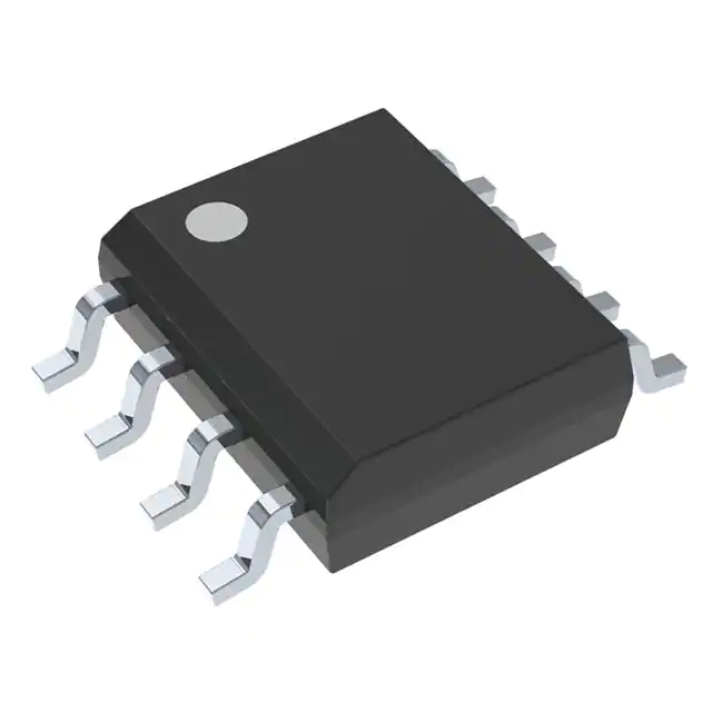
- Part No.:
- MP111DS-LF-Z
- Manufacturer:
- Monolithic Power Systems Inc.
- Category:
- Specialized ICs
- Package:
- 8-SOIC (0.154", 3.90mm Width)
- Datasheet:
-
 MP111DS-LF-Z.pdf
- Description:
- IC STORAGE CAP CONTROL IC 8SOIC
- Quantity:
- Payment:

- Shipping:

Inventory:4,999
Please send an inquiry. Send us your inquiry, and we will respond immediately.
Product details
Overview
MP111DS-LF-Z from Monolithic Power Systems is a dedicated dying gasp storage and release control IC for telecom power backup systems. It charges an external storage capacitor during normal operation (4.5V–18V input), holds voltage up to 32V, and dumps up to 2.5A into VIN when input drops below a user-programmable release threshold. Used in DSL/PON modems to sustain critical communication during AC brownouts.
For engineers reviewing the MP111DS-LF-Z datasheet, MP111DS-LF-Z pinout, MP111DS-LF-Z application, or MP111DS-LF-Z equivalent, this page delivers verified functional role, SOIC-8 package mapping, storage/release voltage programming method, GASP flag behavior, and real-world hold-up time dependencies on CSTORAGE and IRELEASE.
Technical Context
The MP111 implements dual feedback loops: FB1 regulates storage voltage (VSTRG) via external resistor divider; FB2 sets release voltage (VRELEASE) with hysteresis of 50 mV. Charging uses BST-driven boost topology referenced to DC/DC switch node, enabling high-voltage storage without external inductor.
During release, it acts as a controlled current sink from STRG to VIN, maintaining regulated VIN ≈ VRELEASE until VSTRG − VRELEASE falls below ~1V. GASP provides open-drain status signaling with 2 μs delay and 4 mA sink capability at 0.4 V.
Key Specifications
| Parameter | Value and Actual Design Meaning |
|---|---|
| Input Voltage Range | 4.5 V to 18 V - Supports standard telecom DC rails including 12 V PON and 5 V/9 V gateway supplies. |
| Storage Voltage Range | VIN to 32 V max - Enables energy-dense storage using high-voltage electrolytics (e.g., 25 V rated cap at 23 V). |
| Dump Current Limit | 2.5 A - Sustains >1 A load for ≥20 ms with 2000 μF storage cap at 23 V → 10.2 V release. |
| Charge Current Limit | 250 mA - Limits inrush during initial CSTORAGE pre-charge, preventing input rail collapse. |
| Feedback Reference Voltage | 1.0 V ±5% - Sets precision of programmable VSTRG and VRELEASE via resistor dividers. |
| GASP Delay | 2 μs - Ensures fast fault detection and system-level response coordination before power loss escalates. |
| Operating Junction Temp | −40°C to +125°C - Validated for industrial-grade embedded networking equipment operating in uncontrolled environments. |
Pinout & Package
MP111DS-LF-Z is housed in a standard SOIC-8 package (5.0 mm × 6.2 mm, 1.27 mm pitch) with exposed thermal pad not connected internally. Pin functions are validated per MPS MP111 Rev. 1.0 datasheet and confirmed on official Monolithic Power Systems product page.
| Pin/Terminal | Circuit Role | Design Meaning |
|---|---|---|
| 1 - BST | Bootstrap driver output | Connects via RC network to DC/DC switch node to generate gate drive for internal charge pump; enables high-side charging of CSTORAGE. |
| 2 - VIN | Main supply input | 4.5–18 V input rail; powers internal circuitry and serves as dump target; requires local decoupling. |
| 3 - FB2 | Release voltage feedback | Sets VRELEASE threshold; internal comparator triggers dump when VIN < VFB2 × (1 + R3/R4). |
| 4 - GND | System reference ground | Primary return path for all analog and power circuits; must be low-impedance copper plane connection. |
| 5 - FB1 | Storage voltage feedback | Sets VSTRG; internal regulator maintains CSTORAGE at precise voltage during standby. |
| 6 - GASP | Dying gasp status indicator | Open-drain output pulled low when VIN < VRELEASE; used for MCU interrupt or LED alert. |
| 7 - STRG | Storage capacitor terminal | High-current node connecting to positive terminal of main storage capacitor; layout must minimize trace inductance. |
| 8 - VMAX | Internal LDO supply | Requires 2.2 nF ceramic decoupling; powers internal logic and comparators independent of VIN fluctuations. |
Key Features
| Feature | Design Value |
|---|---|
| User-programmable storage voltage | VSTRG set by FB1 resistor divider (e.g., 23 V with R1=845 kΩ, R2=37.4 kΩ); enables optimal capacitor utilization. |
| Programmable release voltage with hysteresis | VRELEASE set by FB2 divider (e.g., 10.2 V with R3=464 kΩ, R4=49.9 kΩ); 50 mV hysteresis prevents chatter during brownout recovery. |
| Integrated 250 mA charge current limiter | Prevents input droop during CSTORAGE pre-charge from 0 V to VIN; eliminates need for external current-limiting FET. |
| 2.5 A regulated dump current | Delivers sustained power to VIN during outage; supports >1 W hold-up loads without external MOSFET or controller. |
| GASP open-drain flag with 2 μs delay | Provides deterministic early-warning signal to host processor before voltage collapse; compatible with 3.3 V or 5 V logic interfaces. |
Applications
| Cable Modem Power Backup | PON Optical Network Terminal |
|---|---|
|
Use Scenario: Maintains DOCSIS registration and upstream transmission during brief AC outages or grid sags in residential cable networks. IC Role / Device Role / Timing Role: Dying gasp controller that sustains 12 V rail for ≥20 ms after input dropout, enabling graceful MAC layer shutdown or emergency packet transmission. Use Value: Prevents service interruption and re-synchronization delays; meets FCC Part 15 Class B immunity requirements for uninterrupted RF transmission. |
Use Scenario: Powers GPON/EPON ONT during utility power loss to maintain optical link and voice-over-IP (VoIP) service for emergency calls. IC Role / Device Role / Timing Role: Energy buffer manager that releases stored charge into 12 V input rail to extend uptime beyond 100 ms, satisfying TR-104 VoIP continuity mandates. Use Value: Eliminates need for supercapacitor-based backup modules; reduces BOM cost and PCB area vs. discrete charge-pump + LDO solutions. |
| DSL Gateway Brownout Protection | Enterprise Wi-Fi Access Point Hold-Up |
|
Use Scenario: Keeps ADSL/VDSL gateway operational during sub-second line voltage dips caused by motor startups or lightning-induced transients. IC Role / Device Role / Timing Role: Input voltage supervisor and charge reservoir controller that activates GASP flag and dumps 2.5 A to stabilize VIN at 9 V for critical PHY and CPU subsystems. Use Value: Avoids router reboot cycles and DHCP lease loss; ensures seamless session persistence for remote management and cloud sync. |
Use Scenario: Provides short-term power retention for 802.11ac access points deployed in commercial buildings with unstable UPS or shared branch circuits. IC Role / Device Role / Timing Role: Standby energy manager that refreshes 22 V storage cap during normal operation and releases charge to 12 V rail upon brownout detection. Use Value: Extends wireless coverage uptime during building-wide power events; supports IEEE 802.3af PoE+ compatibility with minimal external components. |
Equivalent & Alternatives
The following parts are listed as comparable options for similar dying gasp control applications.
| Alternative Part | Technical Difference | Application Difference | Selection Advice |
|---|---|---|---|
| MPQ111DS-AEC1-Z | Automotive-grade variant (AEC-Q100 Grade 1); identical electrical specs but qualified for −40°C to +125°C junction temp with enhanced ESD robustness. | Required for automotive telematics gateways; overqualified for telecom use with higher cost and longer lead times. | Select only if automotive qualification is mandated; no performance benefit in industrial/commercial deployments. |
| TPS65235-1RGET | TI dual-channel hot-swap + backup controller; includes integrated 3.3 V/1.8 V LDOs and I2C interface; dump current limited to 1.5 A. | Targets multi-rail systems needing sequenced power-up; lacks programmable VSTRG/VRELEASE flexibility and GASP flag timing control. | Choose when system requires auxiliary LDOs or digital configuration; avoid if single-rail dying gasp simplicity and 2.5 A dump are primary needs. |
Compared with MPQ111DS-AEC1-Z, the MP111DS-LF-Z offers identical core functionality at lower cost and shorter lead time for non-automotive applications; versus TPS65235-1RGET, it delivers higher dump current, simpler resistor-based programming, and deterministic GASP timing-critical for legacy DSL firmware integration.
Availability
MP111DS-LF-Z is available at Aetrix Electronics and suitable for cable modem power backup, PON optical network terminals, and DSL gateway brownout protection requiring stable component supply across long-lifecycle telecom deployments.
Supply support for MP111DS-LF-Z includes scheduled delivery planning, volume procurement assistance, BOM continuity management, traceable sourcing, and lifecycle availability coordination for OEM customers, industrial embedded developers, connected-device designers, and electronics production programs.
Manufacturer
Monolithic Power Systems (MPS) is a fabless semiconductor company specializing in high-performance analog and power ICs, with design centers in the US, China, and Taiwan, and global manufacturing partnerships.
The MP111 belongs to MPS's Telecom Power Management product line, engineered specifically for reliable, low-component-count dying gasp implementation in broadband access equipment where space, cost, and regulatory compliance are critical constraints.
FAQ
What is the maximum storage voltage the MP111DS-LF-Z can regulate?
The MP111DS-LF-Z supports storage voltages up to 32 V, as specified in its Absolute Maximum Ratings table. This allows use of 25 V-rated electrolytic capacitors at 23 V with 90% derating-enabled by tight regulation and negligible ripple current-reducing required capacitance and board area versus lower-voltage alternatives.
How is the release voltage programmed, and what resistor values yield 10.2 V?
VRELEASE is set by an external resistor divider on FB2: VRELEASE = VFB × (1 + R3/R4). With VFB = 1.0 V typical, R3 = 464 kΩ and R4 = 49.9 kΩ produce 10.2 V. These values are explicitly recommended in Table 2 of the MP111 datasheet for stable operation with 47 μF input capacitance.
Does the MP111DS-LF-Z require an external MOSFET for charge or discharge?
No. The MP111DS-LF-Z integrates all necessary power switches: internal charge pump driven by BST enables high-voltage storage capacitor charging, and an integrated 2.5 A current sink handles regulated discharge from STRG to VIN. No external MOSFETs, drivers, or controllers are needed for basic dying gasp operation.
What is the purpose of the BST pin, and how must it be connected?
BST is the bootstrap driver output that connects-via a series resistor and small ceramic capacitor-to the switch node (SW) of an external DC/DC converter. This connection generates the gate drive voltage needed to operate the internal high-side charge pump. Without SW node coupling, the MP111 cannot initiate storage capacitor charging.
Can the GASP pin directly drive an LED or microcontroller GPIO without additional circuitry?
Yes. GASP is an open-drain output with 4 mA sink capability at 0.4 V, compatible with direct connection to 3.3 V or 5 V logic inputs. For LED indication, connect anode to VIN through a current-limiting resistor (e.g., 1 kΩ for ~3 mA at 12 V); cathode to GASP. No pull-up is required if MCU has internal weak pull-up.
What is the minimum storage capacitance required for 20 ms hold-up at 1 A load?
Using the formula Cs = (IRELEASE × TDASP) / (VSTRG − VRELEASE): with IRELEASE = 1 A, TDASP = 20 ms, VSTRG = 23 V, and VRELEASE = 10.2 V, Cs = 1.56 mF (1560 μF). The datasheet recommends 2000 μF for margin, matching typical xDSL reference designs.
Is thermal shutdown active during dump operation, and what is its threshold?
Yes. Thermal shutdown activates at 150°C junction temperature with 30°C hysteresis (120°C restart), as guaranteed by design. During 2.5 A dump, power dissipation depends on (VSTRG − VRELEASE) × IDUMP; with SOIC-8 θJA = 90°C/W, adequate copper pour and airflow keep TJ well below 150°C for typical 23 V → 10.2 V operation.
MP111DS-LF-Z Specifications
- Product attributes
- Attribute value
- Manufacturer:
- Monolithic Power Systems Inc.
- Series:
- -
- Package/Case:
- 8-SOIC (0.154", 3.90mm Width)
- Packaging:
- Tape & Reel (TR)
- Product Status:
- Not For New Designs
- Programmable:
- Not Verified
- Type:
- Storage Capacitor Control IC
- Applications:
- Cable/DSL/PON Modems
- Mounting Type:
- Surface Mount
- Supplier Device Package:
- 8-SOIC
- Grade:
- -
- Qualification:
- -
MP111DS-LF-Z FAQ
1.How can I place an order for MP111DS-LF-Z through Aetrix?
Please submit a Request for Quotation (RFQ) for MP111DS-LF-Z on Aetrix. Our sales agent will provide a competitive quotation and guide you through the order confirmation once you accept the terms.
2.Are the price and stock information for MP111DS-LF-Z reliable?
The price and inventory of MP111DS-LF-Z are updated periodically and may fluctuate due to market conditions. Stock and pricing data are typically refreshed every 24 hours. Quotation validity for MP111DS-LF-Z is usually 5 days.
3.What payment methods are accepted for MP111DS-LF-Z?
We accept Wire Transfer, PayPal, Credit Card, Western Union, MoneyGram, and Escrow for MP111DS-LF-Z transactions.
Note: Certain payment methods may incur a processing fee.
4.How is shipping managed for MP111DS-LF-Z?
MP111DS-LF-Z orders can be shipped via leading logistics carriers, including DHL, UPS, FedEx, TNT, or Registered Mail.
Once your MP111DS-LF-Z order is processed, you will receive an email with the shipment details and tracking number.
Note: Tracking information may take up to 24 hours to appear. Express delivery typically takes 3–5 business days.
5.How can I obtain technical support or documentation for MP111DS-LF-Z?
For technical support, including MP111DS-LF-Z datasheets, pinout diagrams, or application guidance, please contact our engineering support team. They can provide detailed documentation and assistance for your MP111DS-LF-Z requirements.
6.How does Aetrix verify that MP111DS-LF-Z is sourced from the original manufacturer or authorized distributors?
All MP111DS-LF-Z products on Aetrix are procured from qualified distributors and authorized channels. Our dedicated quality assurance team conducts strict verification, including traceability checks and, if necessary, third-party testing. This ensures that MP111DS-LF-Z meets industry standards.
7.What is the process for return or replacement of MP111DS-LF-Z?
All MP111DS-LF-Z units undergo pre-shipment inspection (PSI). If there is an issue with MP111DS-LF-Z, returns or replacements are accepted under the following conditions:
1.Quantity discrepancies, incorrect items, or visible external defects (such as breakage or corrosion), acknowledged by Aetrix.
2.The issue is reported within 90 days of delivery.
3.The MP111DS-LF-Z part is unused and in its original packaging.
Return procedure for MP111DS-LF-Z:
1.Submit a request within 90 days.
2.Obtain a Return Material Authorization (RMA) from Aetrix.
MP111DS-LF-Z Tags

-
CAP200DG-TL
Power Integrations
-
ATSHA204A-MAHDA-T
Microchip Technology

-
ATSHA204A-SSHDA-T
Microchip Technology

-
ATSHA204A-STUCZ-T
Microchip Technology
-
ATECC608B-MAHDA-T
Microchip Technology
-
ATECC608B-MAHCZ-S
Microchip Technology

-
ATECC608B-SSHDA-T
Microchip Technology
-
ATECC608B-MAHDA-S
Microchip Technology
-
ATECC608A-MAHDA-S
Microchip Technology
-
ATECC608B-MAVDA-T
Microchip Technology

-
ATECC608A-SSHDA-T
Microchip Technology
-
ATECC508A-MAHDA-T
Microchip Technology
Tech Hub

Operational amplifier guide covering op amp basics, feedback, ideal vs real op amps, common configurations, buffer circuits, offset, bias current, gain-bandwidth, slew rate, rail-to-rail limits and sel…

Jumper cables guide covering safe connection order, red and black clamp placement, final ground connection, cable gauge, length, clamp quality, copper vs CCA cables, jump starter comparison and battery…

LDO regulator guide covering low dropout voltage, power dissipation, thermal design, PSRR, output noise, capacitor stability, adjustable LDO circuits, LDO vs buck converter and datasheet selection chec…

Conditional Access Module guide covering CAM meaning, CI/CI+ interface, smart card authorization, DVB security workflow, TV and set-top box compatibility, internal electronics, ESD protection, connecto…

Guide to electronic component obsolescence covering EOL risk, PCN/PDN notices, last-time buy planning, replacement options, form-fit-function validation, counterfeit risk and BOM lifecycle management.

18650 battery guide covering lithium-ion cell basics, 3.6V/3.7V voltage, 4.2V charging, mAh and Wh capacity, protected cells, chargers, BMS, series-parallel packs, holders, welding and sourcing checks.…

Hall effect sensor guide covering working principle, linear and digital sensors, Arduino circuits, current sensing, speed detection, automotive applications, A3144 examples, signal filtering and datash…

Product Change Notification guide for electronic components, covering PCN meaning, PCN vs PDN/EOL, common change types, risk levels, form-fit-function review, engineering validation, BOM control, LTB/L…

A practical guide to blend door actuators, covering HVAC function, symptoms, location, AC and heater issues, reset and calibration, replacement cost, electrical diagnosis, compatibility checks, and rep…

Engineering guide to Raspberry Pi alternatives, covering chip-level differences, Orange Pi, ROCK, Jetson, Banana Pi, NanoPi, Compute Module, Pico, GPIO, camera, HAT compatibility, and replacement risks…


