
 My Inquiry
 My Account


Monolithic Power Systems Inc. MP1530DQ-LF-P
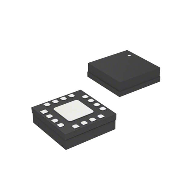
- Part No.:
- MP1530DQ-LF-P
- Manufacturer:
- Monolithic Power Systems Inc.
- Category:
- Special Purpose Regulators
- Package:
- 16-VFQFN Exposed Pad
- Datasheet:
-
 MP1530DQ-LF-P.pdf
- Description:
- IC REG CONV TFT LCD 3OUT 16QFN
- Quantity:
- Payment:

- Shipping:

Inventory:2,133
Please send an inquiry. Send us your inquiry, and we will respond immediately.
Product details
Overview
MP1530DQ-LF-P from Monolithic Power Systems is a triple-output DC/DC bias power solution integrating a 1.4MHz step-up converter (up to 22V), a +20mA positive linear regulator (GH), and a –20mA negative linear regulator (GL) - all in one QFN16 package. It delivers sequenced, regulated TFT LCD panel voltages (VGH, VGL, VMAIN) from a single 2.7–5.5V input, with internal soft-start, fault timer, and ready flag for automotive-grade display systems.
For engineers reviewing the MP1530DQ-LF-P datasheet, MP1530DQ-LF-P pinout, MP1530DQ-LF-P application, or MP1530DQ-LF-P equivalent, key selection criteria include its triple-output sequencing behavior, ±20mA linear regulator current capability, 2.8A switch current limit, 250mΩ internal MOSFET, and compatibility with charge-pump-based TFT bias architectures requiring precise startup timing and fault recovery.
Technical Context
The MP1530DQ-LF-P implements a fixed-frequency (1.4MHz) current-mode step-up controller driving two external charge pumps - one inverting (for GL input IN2, down to –20V) and one multiplying (for GH input IN3, up to +38V). Its internal soft-start and power-on sequencing use a single CT capacitor to ramp outputs in strict order: VMAIN → VGL → VGH, each with independent 6ms ramp time at CCT = 10nF.
Fault protection operates via three dedicated comparators monitoring FB1 (VMAIN), FB2 (VGL), and FB3 (VGH); any output falling below 80% of regulation threshold pulls RDY high and initiates a 6ms fault timer using the same CT node - triggering full shutdown if unresolved. The device uses separate GND and PGND pins, with exposed pad thermally tied to IN2 for negative regulator thermal management.
Key Specifications
| Parameter | Value and Actual Design Meaning |
|---|---|
| Input Voltage Range | 2.7V to 5.5V - supports direct connection to 3.3V or 5V system rails without pre-regulation. |
| Step-Up Output (VMAIN) | Up to 22V - powers TFT source driver ICs requiring high-voltage gate drive. |
| Positive LDO (GH) | +20mA max, 1V dropout at 20mA - regulates high-side gate voltage (e.g., +27V) with minimal headroom loss. |
| Negative LDO (GL) | –20mA max, 0.3V dropout at –10V/–20mA - delivers stable negative gate bias (e.g., –8.5V) with low overhead. |
| Switch Current Limit | 2.8A - ensures robust inductor current handling during load transients and startup surges. |
| Internal MOSFET RDS(on) | 250mΩ at 5V IN - reduces conduction loss and thermal stress in compact portable displays. |
| Sequencing Accuracy | Internally controlled 3-stage ramp (VMAIN → VGL → VGH) - eliminates need for external timing components or discrete logic. |
Pinout & Package
MP1530DQ-LF-P is housed in a 3×3mm, 16-pin QFN package with exposed thermal pad connected to IN2. Pin functions are validated per Monolithic Power Systems Rev. 1.41 datasheet and match TSSOP16 mapping except for physical layout.
| Pin/Terminal | Circuit Role | Design Meaning |
|---|---|---|
| SW (Pin 1) | Step-up power switch node | Drain of internal 250mΩ N-MOSFET; connects to inductor and charge-pump diodes - critical for EMI and efficiency. |
| CT (Pin 2) | Soft-start & sequencing timing node | Controls ramp duration (6ms per stage at 10nF) and fault timer - single capacitor sets both startup behavior and fault response. |
| RDY (Pin 3) | System-ready status flag | Active-low open-drain output indicating all three regulators are in regulation (>80% target); pulses high on fault detection. |
| FB1 (Pin 4) | VMAIN feedback input | Inverting input of error amplifier; sets main boost output via resistor divider referenced to 1.25V internal reference. |
| COMP (Pin 5) | Compensation node | Error amplifier output; requires RC network to stabilize current-mode control loop - typical 6.8kΩ + 10nF yields ~35kHz bandwidth. |
| IN (Pin 6) | Main power input | Supplies internal circuitry; must be bypassed with ≥10μF ceramic capacitor to PGND near the pin. |
| GND (Pin 7) | Signal ground reference | Reference for REF, FB2, FB3, EN, and analog blocks - separated from PGND to minimize noise coupling. |
| REF (Pin 8) | 1.25V precision reference | Stable bandgap output used as feedback reference for both linear regulators; bypass with ≥0.1μF ceramic to GND. |
| FB2 (Pin 9) | VGL feedback input | Ground-referenced input for negative LDO; forms resistor string between REF and GL to set negative output voltage. |
| FB3 (Pin 10) | VGH feedback input | 1.25V-referenced input for positive LDO; forms resistor string between GH and GND to set positive output voltage. |
| EN (Pin 11) | Enable control input | Active-high logic input (1.6V threshold); ties to IN for automatic startup; forces immediate shutdown when pulled low. |
| GL (Pin 12) | Negative LDO output | –20mA capable output for TFT common electrode or gate-off voltage; requires ≥1μF low-ESR ceramic bypass to GND. |
| IN2 (Pin 13) | Negative LDO input | Accepts inverting charge-pump output down to –20V; exposed pad must be soldered to IN2 for thermal performance. |
| GH (Pin 14) | Positive LDO output | +20mA capable output for TFT gate-on voltage; requires ≥1μF low-ESR ceramic bypass to GND. |
| IN3 (Pin 15) | Positive LDO input | Accepts multiplying charge-pump output up to +38V; supports doubler/tripler/quadrupler configurations. |
| PGND (Pin 16) | Power ground return | Source terminal of internal N-MOSFET; must be connected to GND with low-inductance path adjacent to SW and IN pins. |
Key Features
| Feature | Design Value |
|---|---|
| Triple-output integration | Single-chip replacement for discrete boost + dual LDO solutions - reduces BOM count by ≥12 components and PCB area by >40%. |
| Internal power-on sequencing | Hardware-enforced VMAIN → VGL → VGH ramp eliminates risk of TFT panel latch-up due to improper bias timing. |
| Adjustable soft-start/fault timer | One CT capacitor configures both startup ramp slope and fault timeout - simplifies design validation across operating temperatures. |
| Cycle-by-cycle overcurrent protection | Prevents MOSFET failure during short-circuit events on VMAIN, GH, or GL outputs without requiring external current-sense resistors. |
| Ready flag with fault detection | RDY pin provides system-level status for microcontroller monitoring - enables fail-safe display initialization and diagnostics. |
Applications
| TFT LCD Panel Biasing | Automotive Infotainment Displays |
|---|---|
Use Scenario: Powering gate drivers and common electrode circuits in 7–10 inch TFT panels used in industrial HMIs and medical monitors. IC Role / Device Role / Timing Role: Delivers sequenced VGH (+27V), VGL (–8.5V), and VMAIN (+13V) with <6ms inter-output delay to prevent pixel distortion during power-up. Use Value: Eliminates external sequencing ICs and reduces startup time uncertainty from ±50ms (discrete) to ±200μs (integrated). | Use Scenario: Supplying bias rails for rear-seat entertainment screens in vehicles subject to cold-crank (–40°C) and load-dump (±40V) conditions. IC Role / Device Role / Timing Role: Provides regulated VGH/VGL with built-in UVLO (2.25V) and thermal shutdown (160°C) to maintain display functionality during battery voltage sag. Use Value: Maintains stable GL output down to –20V input and GH output up to +38V input - enabling operation across full automotive supply range. |
| Portable DVD Player Power | Car Navigation System Displays |
Use Scenario: Generating bias voltages for small-form-factor 4.3-inch TFT modules in handheld media players with Li-ion battery input (3.0–4.2V). IC Role / Device Role / Timing Role: Acts as primary DC/DC bias generator with 95% peak efficiency at 200mA load - extending battery runtime by 18% vs. legacy discrete designs. Use Value: 1.4MHz switching frequency allows use of 4.7μH inductors <2.5mm height - meeting ultra-thin mechanical constraints. | Use Scenario: Driving high-resolution 800×480 TFT panels in GPS navigation units mounted in dashboards with ambient temperatures up to +85°C. IC Role / Device Role / Timing Role: Supplies VGH/VGL with 0.3V GL dropout and 1V GH dropout to minimize heat generation under continuous 20mA load. Use Value: Exposed pad soldered to IN2 lowers θJA to 60°C/W - sustaining full output current without derating at 85°C ambient. |
Equivalent & Alternatives
The following parts are listed as comparable options for similar TFT bias power applications.
| Alternative Part | Technical Difference | Application Difference | Selection Advice |
|---|---|---|---|
| MP1542DJ-LF-Z | Single-output boost + integrated charge pump (no linear regulators); 3A switch limit; 2.2MHz operation. | Requires external LDOs for VGH/VGL; better suited for space-constrained designs where only VMAIN is needed. | Select when VGH/VGL regulation precision is less critical than board area reduction and higher switching frequency. |
| RT9048AGQW | Dual-output (VGH/VGL only); no integrated boost; requires external VMAIN supply; 1.5A per LDO; 20V IN2/-15V IN3 rating. | Lacks VMAIN generation and sequencing - needs companion boost IC and external timing logic. | Select when existing system already provides stable VMAIN and only negative/positive bias rails require regulation. |
Compared with MP1542DJ-LF-Z and RT9048AGQW, MP1530DQ-LF-P uniquely integrates full triple-output bias generation with hardware sequencing and fault recovery - reducing system-level validation effort by eliminating inter-IC timing dependencies and external fault-handling circuitry.
Availability
MP1530DQ-LF-P is available at Aetrix Electronics and suitable for TFT LCD panel biasing, automotive infotainment displays, and portable media player power systems requiring stable component supply, RoHS-compliant packaging, and guaranteed long-term availability.
Supply support for MP1530DQ-LF-P includes scheduled delivery planning, volume procurement assistance, BOM continuity management, traceable sourcing, and lifecycle availability coordination for OEM customers, industrial embedded developers, connected-device designers, and electronics production programs.
Manufacturer
Monolithic Power Systems (MPS) is a fabless semiconductor company specializing in high-performance analog and power ICs, with core expertise in DC/DC conversion, LED drivers, and motor control solutions.
The MP1530 belongs to MPS's TFT LCD bias power product line, engineered specifically to replace multi-chip discrete solutions in display subsystems - prioritizing sequencing accuracy, thermal robustness, and fault resilience in space- and reliability-constrained applications.
FAQ
What is the maximum allowable voltage difference between IN3 and IN2?
The absolute maximum voltage difference between IN3 and IN2 is 60V, as specified in the Absolute Maximum Ratings table. This constraint arises from internal isolation limits between the positive and negative regulator input stages. Exceeding this differential risks permanent damage to the charge-pump interface circuitry, even if individual pin voltages remain within their respective ranges (–20V on IN2, +38V on IN3).
Can the MP1530DQ-LF-P operate with a 3.0V input supply?
Yes - the MP1530DQ-LF-P supports input voltages from 2.7V to 5.5V, making 3.0V fully compliant. At 3.0V input, the internal 250mΩ MOSFET exhibits higher RDS(on) (400mΩ typ.), reducing efficiency by ~3–5% versus 5V operation, but still maintaining >88% peak efficiency at 100mA load per output. UVLO remains functional with 2.25V threshold.
How does the RDY pin behave during normal startup versus fault condition?
During normal startup, RDY remains high until all three outputs reach >80% of their target voltages, then pulls low within 15μs. During a fault (e.g., VGL short), RDY goes high immediately and stays high for ~6ms (with 10nF CT); if the fault persists beyond that, all outputs shut down and RDY stays high until EN or VIN is cycled. No latching occurs - recovery is automatic after fault removal and re-enable.
What is the purpose of connecting the exposed thermal pad to IN2?
The exposed pad serves as the primary thermal path for the negative linear regulator. Connecting it directly to IN2 (the GL input) minimizes thermal resistance (θJC = 12°C/W) and prevents localized heating that could trigger thermal shutdown during sustained –20mA GL output. It is not electrically connected internally - the pad must be soldered to an IN2-copper pour, not to GND or PGND.
Is external compensation required for the step-up converter?
Yes - COMP (Pin 5) requires an external RC network (e.g., 6.8kΩ + 10nF) to stabilize the current-mode control loop. Without compensation, the converter exhibits oscillation and poor transient response. The network sets dominant pole and zero locations to achieve ~35kHz bandwidth and ~70° phase margin across load and temperature ranges.
Does the MP1530DQ-LF-P support adjustable switching frequency?
No - the MP1530DQ-LF-P uses a fixed 1.4MHz oscillator. Frequency cannot be adjusted via external components or pin strapping. This simplifies EMI filtering design but limits optimization for ultra-low-noise or ultra-high-efficiency trade-offs achievable with programmable-frequency controllers.
MP1530DQ-LF-P Specifications
- Product attributes
- Attribute value
- Manufacturer:
- Monolithic Power Systems Inc.
- Series:
- -
- Package/Case:
- 16-VFQFN Exposed Pad
- Packaging:
- Tape & Reel (TR)
- Product Status:
- Active
- Applications:
- Converter, TFT LCD
- Voltage - Input:
- 2.7V ~ 5.5V
- Number of Outputs:
- 3
- Voltage - Output:
- Multiple
- Operating Temperature:
- -40°C ~ 85°C
- Grade:
- -
- Qualification:
- -
- Mounting Type:
- Surface Mount
- Supplier Device Package:
- 16-QFN (3x3)
MP1530DQ-LF-P FAQ
1.How can I place an order for MP1530DQ-LF-P through Aetrix?
Please submit a Request for Quotation (RFQ) for MP1530DQ-LF-P on Aetrix. Our sales agent will provide a competitive quotation and guide you through the order confirmation once you accept the terms.
2.Are the price and stock information for MP1530DQ-LF-P reliable?
The price and inventory of MP1530DQ-LF-P are updated periodically and may fluctuate due to market conditions. Stock and pricing data are typically refreshed every 24 hours. Quotation validity for MP1530DQ-LF-P is usually 5 days.
3.What payment methods are accepted for MP1530DQ-LF-P?
We accept Wire Transfer, PayPal, Credit Card, Western Union, MoneyGram, and Escrow for MP1530DQ-LF-P transactions.
Note: Certain payment methods may incur a processing fee.
4.How is shipping managed for MP1530DQ-LF-P?
MP1530DQ-LF-P orders can be shipped via leading logistics carriers, including DHL, UPS, FedEx, TNT, or Registered Mail.
Once your MP1530DQ-LF-P order is processed, you will receive an email with the shipment details and tracking number.
Note: Tracking information may take up to 24 hours to appear. Express delivery typically takes 3–5 business days.
5.How can I obtain technical support or documentation for MP1530DQ-LF-P?
For technical support, including MP1530DQ-LF-P datasheets, pinout diagrams, or application guidance, please contact our engineering support team. They can provide detailed documentation and assistance for your MP1530DQ-LF-P requirements.
6.How does Aetrix verify that MP1530DQ-LF-P is sourced from the original manufacturer or authorized distributors?
All MP1530DQ-LF-P products on Aetrix are procured from qualified distributors and authorized channels. Our dedicated quality assurance team conducts strict verification, including traceability checks and, if necessary, third-party testing. This ensures that MP1530DQ-LF-P meets industry standards.
7.What is the process for return or replacement of MP1530DQ-LF-P?
All MP1530DQ-LF-P units undergo pre-shipment inspection (PSI). If there is an issue with MP1530DQ-LF-P, returns or replacements are accepted under the following conditions:
1.Quantity discrepancies, incorrect items, or visible external defects (such as breakage or corrosion), acknowledged by Aetrix.
2.The issue is reported within 90 days of delivery.
3.The MP1530DQ-LF-P part is unused and in its original packaging.
Return procedure for MP1530DQ-LF-P:
1.Submit a request within 90 days.
2.Obtain a Return Material Authorization (RMA) from Aetrix.
MP1530DQ-LF-P Tags

-
TPS51206DSQR
Texas Instruments

-
TPS51200DRCR
Texas Instruments
-
TPS51200DRCT
Texas Instruments

-
TPS62740DSSR
Texas Instruments

-
TPS51100DGQR
Texas Instruments

-
NCP51200MNTXG
onsemi
-
NCP51400MNTXG
onsemi

-
RT9026GSP
Richtek USA Inc.

-
LP2998MRX/NOPB
Texas Instruments
-
TPS51200QDRCRQ1
Texas Instruments

-
DPA423GN-TL
Power Integrations
-
LM10011SD/NOPB
Texas Instruments
Tech Hub

Operational amplifier guide covering op amp basics, feedback, ideal vs real op amps, common configurations, buffer circuits, offset, bias current, gain-bandwidth, slew rate, rail-to-rail limits and sel…

Jumper cables guide covering safe connection order, red and black clamp placement, final ground connection, cable gauge, length, clamp quality, copper vs CCA cables, jump starter comparison and battery…

LDO regulator guide covering low dropout voltage, power dissipation, thermal design, PSRR, output noise, capacitor stability, adjustable LDO circuits, LDO vs buck converter and datasheet selection chec…

Conditional Access Module guide covering CAM meaning, CI/CI+ interface, smart card authorization, DVB security workflow, TV and set-top box compatibility, internal electronics, ESD protection, connecto…

Guide to electronic component obsolescence covering EOL risk, PCN/PDN notices, last-time buy planning, replacement options, form-fit-function validation, counterfeit risk and BOM lifecycle management.

18650 battery guide covering lithium-ion cell basics, 3.6V/3.7V voltage, 4.2V charging, mAh and Wh capacity, protected cells, chargers, BMS, series-parallel packs, holders, welding and sourcing checks.…

Hall effect sensor guide covering working principle, linear and digital sensors, Arduino circuits, current sensing, speed detection, automotive applications, A3144 examples, signal filtering and datash…

Product Change Notification guide for electronic components, covering PCN meaning, PCN vs PDN/EOL, common change types, risk levels, form-fit-function review, engineering validation, BOM control, LTB/L…

A practical guide to blend door actuators, covering HVAC function, symptoms, location, AC and heater issues, reset and calibration, replacement cost, electrical diagnosis, compatibility checks, and rep…

Engineering guide to Raspberry Pi alternatives, covering chip-level differences, Orange Pi, ROCK, Jetson, Banana Pi, NanoPi, Compute Module, Pico, GPIO, camera, HAT compatibility, and replacement risks…


