
 My Inquiry
 My Account


Monolithic Power Systems Inc. MP1531DQ-LF-P
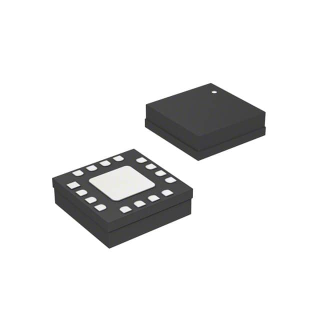
- Part No.:
- MP1531DQ-LF-P
- Manufacturer:
- Monolithic Power Systems Inc.
- Category:
- Special Purpose Regulators
- Package:
- 16-VFQFN Exposed Pad
- Datasheet:
-
 MP1531DQ-LF-P.pdf
- Description:
- IC REG CONV TFT LCD 3OUT 16QFN
- Quantity:
- Payment:

- Shipping:

Inventory:4,739
Please send an inquiry. Send us your inquiry, and we will respond immediately.
Product details
Overview
MP1531DQ-LF-P from Monolithic Power Systems is a triple-output DC/DC converter IC for TFT LCD bias generation, integrating a 250kHz fixed-frequency step-up converter (up to 22V), a ±10mA linear regulator pair (GH up to +38V, GL down to –20V), and internal power-on sequencing-all in a 3×3mm QFN-16 package. It operates from 2.7V–5.5V input and delivers regulated VGH/VGL/VMAIN for active-matrix display panels.
For engineers reviewing the MP1531DQ-LF-P datasheet, MP1531DQ-LF-P pinout, MP1531DQ-LF-P application, or MP1531DQ-LF-P equivalent, key selection criteria include its integrated charge-pump–driven linear regulators, 1μA shutdown current, internal soft-start timing control via CT pin, and fault-sensing RDY flag with 6ms timeout-critical for reliable TFT panel power-up in portable displays.
Technical Context
The MP1531DQ-LF-P implements a current-mode controlled step-up converter with 250mΩ internal N-channel MOSFET switch and cycle-by-cycle overcurrent protection. Its feedback architecture uses separate error amplifiers for main output (FB1), positive regulator (FB3), and negative regulator (FB2), each referenced to 1.25V (FB1/FB3) or GND (FB2).
Power-on sequencing is hardware-controlled: step-up converter enables first, followed by GL (negative regulator), then GH (positive regulator), all ramped via CT capacitor timing. Fault detection monitors FB voltages; if any falls below 80% of regulation threshold for >6ms (CT = 10nF), all outputs shut down and RDY goes high-impedance.
Key Specifications
| Parameter | Value and Actual Design Meaning |
|---|---|
| Input Voltage Range | 2.7V to 5.5V - supports single-cell Li-ion (3.0–4.2V) and USB-powered systems without external LDO pre-regulation. |
| Step-Up Output (VMAIN) | Up to 22V - sufficient for TFT gate driver supply in mid-size panels; regulated via FB1 with 1.25V reference. |
| Positive Regulator (GH) | +38V max input, +10mA output - powers TFT VGH with dropout as low as 0.5V at 10mA, enabling high-voltage bias from charge-pump stages. |
| Negative Regulator (GL) | –20V min input, –10mA output - supplies TFT VGL with 0.15V dropout at 10mA, supporting deep-negative bias for wide-temperature LCDs. |
| Switching Frequency | Fixed 250kHz - enables compact 1–4.7μH inductors and reduces EMI compared to sub-100kHz boost converters. |
| Shutdown Current | 1μA - minimizes battery drain in always-on display standby modes, critical for portable DVD and navigation units. |
| Thermal Protection | 160°C junction shutdown - prevents damage during sustained overload or poor PCB thermal layout; auto-recovery requires EN or VIN cycling. |
Pinout & Package
MP1531DQ-LF-P is housed in a thermally enhanced 16-pin QFN package (3mm × 3mm, 0.5mm pitch) with exposed pad soldered to IN2 (–20V node) for optimal heat dissipation and noise isolation.
| Pin/Terminal | Circuit Role | Design Meaning |
|---|---|---|
| SW (Pin 1) | Step-up converter switch node | Drain of internal 250mΩ N-MOSFET; connects to inductor and charge-pump diodes-requires low-inductance routing to minimize switching loss and EMI. |
| CT (Pin 2) | Soft-start & sequencing timing | Capacitor-to-GND sets 6ms soft-start ramp per stage (9ms total sequencing); also defines 6ms fault timer window. |
| RDY (Pin 3) | Fault status indicator | Open-drain output pulled low only when all three outputs are within 80% of regulation; high-impedance indicates startup or fault condition. |
| FB1 (Pin 4) | Main boost output feedback | Inverting input of error amplifier; 1.25V threshold sets VMAIN via resistive divider-enables precise, stable gate drive voltage. |
| COMP (Pin 5) | Compensation node | Error amplifier output; external RC network (e.g., 5.6kΩ + 10nF) stabilizes loop with ~70° phase margin and 35kHz bandwidth. |
| IN (Pin 6) | Main power input | Supplies internal circuitry; requires ≥10μF low-ESR ceramic bypass to PGND near pin to suppress input ripple and noise. |
| GND (Pin 7) | Signal ground reference | Low-noise analog reference for REF, FB pins, and error amplifiers-must be separated from PGND and joined at single point. |
| REF (Pin 8) | 1.25V precision reference | Stable bandgap output used as feedback reference for GL regulator; bypass with ≥0.1μF ceramic to GND for noise immunity. |
| FB2 (Pin 9) | Negative regulator feedback | Connects between REF and GL; GND-referenced threshold enables programmable VGL from –0.15V to –20V with 10mA load capability. |
| FB3 (Pin 10) | Positive regulator feedback | 1.25V-referenced input for GH; sets VGH from +0.5V to +38V using resistor divider from GH to GND. |
| EN (Pin 11) | Enable control input | Active-high logic; 1.6V threshold allows direct connection to microcontroller GPIO or VIN for automatic startup. |
| GL (Pin 12) | Negative linear regulator output | Delivers up to –10mA at user-programmed voltage; requires ≥1μF low-ESR ceramic bypass to GND for stability. |
| IN2 (Pin 13) | Negative regulator input | Driven by inverting charge pump from SW; rated to –20V-exposed pad must connect to this pin for thermal performance. |
| GH (Pin 14) | Positive linear regulator output | Delivers up to +10mA at user-programmed voltage; bypass with ≥1μF low-ESR ceramic to GND to suppress output ripple. |
| IN3 (Pin 15) | Positive regulator input | Driven by doubler/tripler/quadrupler charge pump from SW; rated to +38V-supports high-VGH with minimal external components. |
| PGND (Pin 16) | Power ground return | Source of internal N-MOSFET; must connect directly to input capacitor ground and inductor ground with short, wide trace to minimize switching noise. |
Key Features
| Feature | Design Value |
|---|---|
| Triple-output integration | Single-chip solution replaces discrete boost + dual LDO + external charge-pump controllers-reduces BOM count by ≥12 components and saves ≥25mm² PCB area. |
| Hardware-based power sequencing | Internal state machine sequences VMAIN → VGL → VGH with synchronized soft-start ramps-eliminates need for external timers or MCU intervention during panel initialization. |
| Charge-pump–driven linear regulators | GL and GH powered directly from SW node via external diode-cap networks-avoids dedicated high-voltage charge-pump ICs and simplifies layout for TFT bias rails. |
| Fault detection with auto-shutdown | RDY pin and CT-based 6ms fault timer detect undervoltage on any output and disable all regulators-prevents partial panel operation that could cause image artifacts or latch-up. |
| Ultra-low shutdown current | 1μA quiescent draw in shutdown mode-extends battery life in portable devices where display may remain connected but inactive for hours. |
Applications
| Automotive Infotainment Displays | Industrial Handheld Terminals |
|---|---|
Use Scenario: Car navigation system with 7-inch TFT LCD requiring stable VGH (+18V), VGL (–10V), and VMAIN (+5V) under cold-crank (5.5V) and alternator surge (16V) conditions. IC Role / Device Role / Timing Role: MP1531DQ-LF-P acts as primary TFT bias generator, delivering sequenced, regulated outputs independent of input rail fluctuations; RDY flag synchronizes MCU display enable after full power-up. Use Value: Internal UVLO (2.25V) and thermal shutdown prevent malfunction during engine start; 95% peak efficiency extends runtime on 12V battery backup. | Use Scenario: Ruggedized warehouse scanner with sunlight-readable TFT display operating from 3.7V Li-ion battery across –20°C to +70°C ambient. IC Role / Device Role / Timing Role: Provides temperature-stable VGH/VGL bias despite battery voltage sag to 2.8V; GL's –20V capability ensures consistent contrast at low temperatures. Use Value: 1μA shutdown current preserves battery charge during idle; QFN-16 package withstands mechanical shock and thermal cycling better than TSSOP alternatives. |
| Portable Medical Imaging Devices | Avionics Display Units |
Use Scenario: Battery-powered ultrasound tablet with high-resolution TFT requiring flicker-free VGH/VGL with <1% output drift during imaging bursts. IC Role / Device Role / Timing Role: Delivers low-noise, sequenced bias rails; COMP compensation network maintains >70° phase margin under dynamic load steps from column drivers. Use Value: Cycle-by-cycle current limit protects against inductor saturation during rapid panel refresh; 0.15V GL dropout ensures stable black-level voltage at full load. | Use Scenario: FAA-certified cockpit display with dual-redundant power paths and strict EMI limits; requires fail-safe bias generation with deterministic shutdown behavior. IC Role / Device Role / Timing Role: Serves as certified bias source with RDY flag feeding aircraft health monitoring system; fault timer provides predictable 6ms response window for system-level fault logging. Use Value: Exposed-pad QFN thermal design meets DO-160E thermal soak requirements; 250kHz switching avoids critical avionics bands (e.g., 118–137MHz comms). |
Equivalent & Alternatives
The following parts are listed as comparable options for similar TFT LCD bias generator applications.
| Alternative Part | Technical Difference | Application Difference | Selection Advice |
|---|---|---|---|
| MAX17105ETJ+ | Quad-output (VPOS/VNEG/VCOM/VDD) with integrated gate drivers; 2.7–5.5V input; no internal sequencing-requires external timing control. | Supports larger panels with VCOM calibration; lacks hardware power-on sequence-increases firmware complexity for display initialization. | Select when VCOM generation or higher current (>15mA) is required; avoid if minimizing MCU overhead is critical. |
| RT9397BF | Dual-output (VGH/VGL) only; no main boost converter; requires external 5V supply; 1.2–5.5V input range; 2.5MHz switching. | Optimized for ultra-thin designs with pre-regulated 5V rail; cannot replace MP1531DQ-LF-P in single-battery systems needing VMAIN generation. | Select for space-constrained applications with existing 5V bias rail; not suitable as drop-in replacement for battery-fed TFT systems. |
Compared with MAX17105ETJ+ and RT9397BF, MP1531DQ-LF-P uniquely integrates triple-output generation with autonomous sequencing and charge-pump–fed linear regulators-reducing external component count and eliminating software-dependent startup coordination required by alternatives.
Availability
MP1531DQ-LF-P is available at Aetrix Electronics and suitable for automotive infotainment displays, industrial handheld terminals, and portable medical imaging devices requiring stable component supply and long-term lifecycle support.
Supply support for MP1531DQ-LF-P includes scheduled delivery planning, volume procurement assistance, BOM continuity management, traceable sourcing, and lifecycle availability coordination for OEM customers, industrial embedded developers, connected-device designers, and electronics production programs.
Manufacturer
Monolithic Power Systems (MPS) is a fabless semiconductor company specializing in high-performance analog and power ICs, with core expertise in DC/DC conversion, motor drivers, and LED lighting controllers.
The MP1531 product line targets TFT LCD bias generation for portable and automotive displays, emphasizing integration, sequencing reliability, and low-quiescent-power operation in compact packages.
FAQ
What is the maximum allowable voltage difference between IN3 and IN2 pins?
The absolute maximum voltage difference between IN3 and IN2 is 60V, as specified in the Absolute Maximum Ratings table. This constraint arises from internal isolation limits of the charge-pump–driven linear regulator inputs and must be respected to prevent device damage-even if individual pin ratings (IN3 to +38V, IN2 to –20V) suggest higher differential tolerance.
Can the MP1531DQ-LF-P generate VGH = +25V and VGL = –15V simultaneously from a 3.3V input?
Yes. With appropriate external charge-pump diodes and flying capacitors, the MP1531DQ-LF-P can achieve +25V on GH (using a tripler configuration from SW) and –15V on GL (using a 2x inverter). The datasheet confirms IN3 supports up to +38V and IN2 down to –20V, and both linear regulators deliver ±10mA at those extremes with specified dropout voltages.
How does the RDY pin behave during normal operation versus fault condition?
During normal operation, RDY is actively pulled low after successful power-on sequencing and remains low as long as all FB voltages stay above 80% of their thresholds. During a fault (e.g., open feedback resistor), RDY transitions to high-impedance within ~15μs and stays there until either the fault clears or the 6ms CT-based timer expires-triggering full shutdown.
Is the exposed thermal pad on the QFN package electrically connected?
No. The exposed pad has no internal electrical connection but must be soldered to the IN2 net (–20V node) per the datasheet. This provides optimal thermal conduction path while maintaining electrical isolation-critical for safe operation given IN2's negative voltage swing and the pad's role in reducing θJA from 60°C/W to effective ~35°C/W in typical layouts.
What is the minimum recommended output capacitor for the step-up converter?
A 10μF ceramic capacitor is the minimum recommended value for the step-up converter output, as stated in the Application Information section. Lower values risk instability and excessive ripple; ceramic type is mandatory due to low ESR requirements-tantalum or aluminum electrolytics are unsuitable for this high-frequency, current-mode topology.
Does the MP1531DQ-LF-P support adjustable switching frequency?
No. The MP1531DQ-LF-P uses a fixed 250kHz oscillator with ±20% tolerance (200–300kHz). Frequency adjustment is not supported-unlike some competing boost controllers, it lacks an external resistor or capacitor frequency programming option. Layout and component selection must accommodate this fixed frequency for EMI filtering and inductor sizing.
How is power-on sequencing initiated-by EN pin or input voltage rise?
Sequencing initiates on either event: a rising edge on EN (≥1.6V) or VIN crossing the 2.25V UVLO threshold while EN is high. Both paths trigger the same internal state machine-first ramping VMAIN, then GL, then GH-ensuring deterministic startup whether controlled by MCU or battery insertion.
MP1531DQ-LF-P Specifications
- Product attributes
- Attribute value
- Manufacturer:
- Monolithic Power Systems Inc.
- Series:
- -
- Package/Case:
- 16-VFQFN Exposed Pad
- Packaging:
- Tape & Reel (TR)
- Product Status:
- Not For New Designs
- Applications:
- Converter, TFT LCD
- Voltage - Input:
- 2.7V ~ 5.5V
- Number of Outputs:
- 3
- Voltage - Output:
- Multiple
- Operating Temperature:
- -40°C ~ 85°C
- Grade:
- -
- Qualification:
- -
- Mounting Type:
- Surface Mount
- Supplier Device Package:
- 16-QFN (3x3)
MP1531DQ-LF-P FAQ
1.How can I place an order for MP1531DQ-LF-P through Aetrix?
Please submit a Request for Quotation (RFQ) for MP1531DQ-LF-P on Aetrix. Our sales agent will provide a competitive quotation and guide you through the order confirmation once you accept the terms.
2.Are the price and stock information for MP1531DQ-LF-P reliable?
The price and inventory of MP1531DQ-LF-P are updated periodically and may fluctuate due to market conditions. Stock and pricing data are typically refreshed every 24 hours. Quotation validity for MP1531DQ-LF-P is usually 5 days.
3.What payment methods are accepted for MP1531DQ-LF-P?
We accept Wire Transfer, PayPal, Credit Card, Western Union, MoneyGram, and Escrow for MP1531DQ-LF-P transactions.
Note: Certain payment methods may incur a processing fee.
4.How is shipping managed for MP1531DQ-LF-P?
MP1531DQ-LF-P orders can be shipped via leading logistics carriers, including DHL, UPS, FedEx, TNT, or Registered Mail.
Once your MP1531DQ-LF-P order is processed, you will receive an email with the shipment details and tracking number.
Note: Tracking information may take up to 24 hours to appear. Express delivery typically takes 3–5 business days.
5.How can I obtain technical support or documentation for MP1531DQ-LF-P?
For technical support, including MP1531DQ-LF-P datasheets, pinout diagrams, or application guidance, please contact our engineering support team. They can provide detailed documentation and assistance for your MP1531DQ-LF-P requirements.
6.How does Aetrix verify that MP1531DQ-LF-P is sourced from the original manufacturer or authorized distributors?
All MP1531DQ-LF-P products on Aetrix are procured from qualified distributors and authorized channels. Our dedicated quality assurance team conducts strict verification, including traceability checks and, if necessary, third-party testing. This ensures that MP1531DQ-LF-P meets industry standards.
7.What is the process for return or replacement of MP1531DQ-LF-P?
All MP1531DQ-LF-P units undergo pre-shipment inspection (PSI). If there is an issue with MP1531DQ-LF-P, returns or replacements are accepted under the following conditions:
1.Quantity discrepancies, incorrect items, or visible external defects (such as breakage or corrosion), acknowledged by Aetrix.
2.The issue is reported within 90 days of delivery.
3.The MP1531DQ-LF-P part is unused and in its original packaging.
Return procedure for MP1531DQ-LF-P:
1.Submit a request within 90 days.
2.Obtain a Return Material Authorization (RMA) from Aetrix.
MP1531DQ-LF-P Tags

-
TPS51206DSQR
Texas Instruments

-
TPS51200DRCR
Texas Instruments
-
TPS51200DRCT
Texas Instruments

-
TPS62740DSSR
Texas Instruments

-
TPS51100DGQR
Texas Instruments

-
NCP51200MNTXG
onsemi
-
NCP51400MNTXG
onsemi

-
RT9026GSP
Richtek USA Inc.

-
LP2998MRX/NOPB
Texas Instruments
-
TPS51200QDRCRQ1
Texas Instruments

-
DPA423GN-TL
Power Integrations
-
LM10011SD/NOPB
Texas Instruments
Tech Hub

Operational amplifier guide covering op amp basics, feedback, ideal vs real op amps, common configurations, buffer circuits, offset, bias current, gain-bandwidth, slew rate, rail-to-rail limits and sel…

Jumper cables guide covering safe connection order, red and black clamp placement, final ground connection, cable gauge, length, clamp quality, copper vs CCA cables, jump starter comparison and battery…

LDO regulator guide covering low dropout voltage, power dissipation, thermal design, PSRR, output noise, capacitor stability, adjustable LDO circuits, LDO vs buck converter and datasheet selection chec…

Conditional Access Module guide covering CAM meaning, CI/CI+ interface, smart card authorization, DVB security workflow, TV and set-top box compatibility, internal electronics, ESD protection, connecto…

Guide to electronic component obsolescence covering EOL risk, PCN/PDN notices, last-time buy planning, replacement options, form-fit-function validation, counterfeit risk and BOM lifecycle management.

18650 battery guide covering lithium-ion cell basics, 3.6V/3.7V voltage, 4.2V charging, mAh and Wh capacity, protected cells, chargers, BMS, series-parallel packs, holders, welding and sourcing checks.…

Hall effect sensor guide covering working principle, linear and digital sensors, Arduino circuits, current sensing, speed detection, automotive applications, A3144 examples, signal filtering and datash…

Product Change Notification guide for electronic components, covering PCN meaning, PCN vs PDN/EOL, common change types, risk levels, form-fit-function review, engineering validation, BOM control, LTB/L…

A practical guide to blend door actuators, covering HVAC function, symptoms, location, AC and heater issues, reset and calibration, replacement cost, electrical diagnosis, compatibility checks, and rep…

Engineering guide to Raspberry Pi alternatives, covering chip-level differences, Orange Pi, ROCK, Jetson, Banana Pi, NanoPi, Compute Module, Pico, GPIO, camera, HAT compatibility, and replacement risks…


