
 My Inquiry
 My Account


Monolithic Power Systems Inc. MP1531DQ-LF-Z
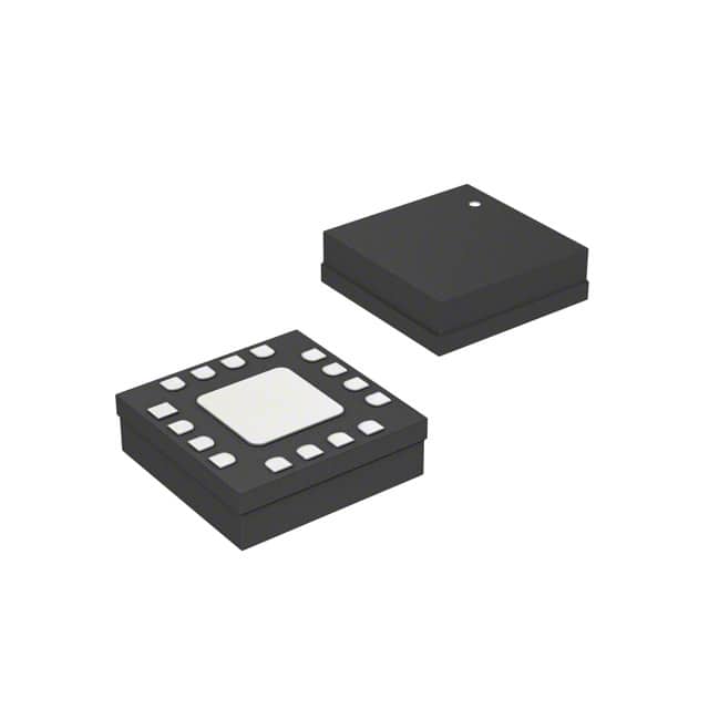
- Part No.:
- MP1531DQ-LF-Z
- Manufacturer:
- Monolithic Power Systems Inc.
- Category:
- Special Purpose Regulators
- Package:
- 16-VFQFN Exposed Pad
- Datasheet:
-
 MP1531DQ-LF-Z.pdf
- Description:
- IC REG CONV TFT LCD 3OUT 16QFN
- Quantity:
- Payment:

- Shipping:

Inventory:4,272
Please send an inquiry. Send us your inquiry, and we will respond immediately.
Product details
Overview
MP1531DQ-LF-Z from Monolithic Power Systems is a triple-output DC/DC bias power solution for TFT LCD panels, integrating a 250kHz fixed-frequency step-up converter (up to 22V), a ±10mA linear regulator pair (GH up to +38V, GL down to –20V), and internal power-on sequencing-all in a 3×3mm QFN-16 package. It operates from 2.7V–5.5V input and delivers coordinated VGH/VGL/VMAIN rails for display driver ICs.
For engineers reviewing the MP1531DQ-LF-Z datasheet, MP1531DQ-LF-Z pinout, MP1531DQ-LF-Z application, or MP1531DQ-LF-Z equivalent, key selection criteria include its integrated charge-pump–driven linear regulators, internal soft-start timing via CT pin, RDY fault signaling, and dual-input voltage range compatibility with Li-ion and USB-powered portable displays.
Technical Context
The MP1531DQ-LF-Z implements current-mode control in its 250kHz step-up converter for fast transient response and stable regulation under dynamic load conditions typical of TFT gate drivers. Its GH and GL linear regulators are powered by external charge-pump stages driven from the SW node-positive pump configurable as doubler/tripler/quadrupler, negative pump as inverter-enabling wide output voltage flexibility.
Internal sequencing ensures safe power-up order: step-up converter first, then GL (negative rail), then GH (positive rail), each with independent soft-start ramp controlled by the CT capacitor. Fault detection monitors FB1/FB2/FB3 voltages; if any falls below 80% of regulation threshold for >6ms (CT = 10nF), all outputs disable and RDY goes high-impedance.
Key Specifications
| Parameter | Value and Actual Design Meaning |
|---|---|
| Input Voltage Range | 2.7V to 5.5V - supports single-cell Li-ion (3.0–4.2V) and USB 5V systems without LDO pre-regulation. |
| Step-Up Output (VMAIN) | Up to 22V - powers main TFT source driver supply; regulated via FB1 feedback with 1.25V reference. |
| Positive Regulator (GH) | +38V max output - supplies TFT gate-on voltage (VGH); uses P-channel pass element with FB3 = 1.25V threshold. |
| Negative Regulator (GL) | –20V min output - supplies TFT gate-off voltage (VGL); uses N-channel pass element with FB2 referenced to GND. |
| Switch Current Limit | 0.5A - limits peak inductor current during startup and overload, preventing MOSFET stress and ensuring reliable boost operation. |
| Efficiency | 95% peak - achieved at light-to-moderate loads due to low RDS(on) (250mΩ) switch and optimized charge-pump topology. |
| Shutdown Current | 1μA - enables ultra-low-power standby in battery-operated devices such as portable navigation units. |
Pinout & Package
MP1531DQ-LF-Z is housed in a thermally enhanced 16-pin QFN package (3mm × 3mm, 0.5mm pitch) with exposed pad connected to IN2 for optimal thermal performance in TFT bias applications.
| Pin/Terminal | Circuit Role | Design Meaning |
|---|---|---|
| SW (Pin 1) | Step-up converter switch node | Drain of internal 250mΩ N-MOSFET; drives external inductor and charge-pump diodes; critical for EMI and thermal layout. |
| CT (Pin 2) | Soft-start and sequencing timer | Connects to GND via capacitor (e.g., 10nF) to set 6ms soft-start ramp and 6ms fault timeout; shared timing resource. |
| RDY (Pin 3) | Fault status indicator | Open-drain output pulled low when all outputs are in regulation (>80% of target); high-impedance on fault or startup. |
| FB1 (Pin 4) | Main boost feedback input | Inverting input of error amplifier; sets VMAIN via resistor divider; 1.25V regulation threshold. |
| COMP (Pin 5) | Compensation node | Error amplifier output; requires RC network (e.g., 5.6kΩ + 10nF) to stabilize current-mode loop with ~35kHz bandwidth. |
| IN (Pin 6) | Main power input | Supplies internal circuitry; bypass with ≥10μF ceramic capacitor close to PGND to suppress switching noise. |
| GND (Pin 7) | Signal ground reference | Reference for REF, FB2, FB3, EN; must be separated from PGND and joined at single point near IC. |
| REF (Pin 8) | 1.25V precision reference | Stable 1.25V output used as feedback reference for GL regulator; bypass with ≥0.1μF ceramic capacitor. |
| FB2 (Pin 9) | Negative regulator feedback | Connects between REF and GL to set VGL; regulation threshold is GND - enables precise negative rail generation. |
| FB3 (Pin 10) | Positive regulator feedback | Connects between GH and GND to set VGH; regulation threshold is 1.25V - standard for positive LDO configuration. |
| EN (Pin 11) | Enable control input | Active-high logic input; rising edge initiates full power-on sequence; can be tied to IN for automatic startup. |
| GL (Pin 12) | Negative linear regulator output | Delivers up to –20V/10mA; requires ≥1μF low-ESR ceramic bypass to GND for stability and ripple suppression. |
| IN2 (Pin 13) | Negative regulator input | Driven by inverting charge-pump from SW; accepts –20V; exposed pad soldered to this pin for thermal relief. |
| GH (Pin 14) | Positive linear regulator output | Delivers up to +38V/10mA; requires ≥1μF low-ESR ceramic bypass to GND; critical for TFT gate drive integrity. |
| IN3 (Pin 15) | Positive regulator input | Driven by multiplying charge-pump from SW; accepts up to +38V; determines maximum achievable VGH. |
| PGND (Pin 16) | Power ground return | Source of internal MOSFET; must connect directly to low-inductance ground plane adjacent to SW and IN pins. |
Key Features
| Feature | Design Value |
|---|---|
| Integrated triple-rail bias generation | Eliminates need for three discrete DC/DC converters - reduces BOM count, PCB area, and design complexity for TFT panel power. |
| Internal power-on sequencing | Guarantees safe startup order (VMAIN → VGL → VGH) without external controllers or timers - prevents latch-up in display driver ICs. |
| Adjustable soft-start/fault timer | Single CT pin configures both startup ramp duration and fault timeout period - simplifies timing design and improves system reliability. |
| Ready flag with fault detection | RDY pin provides system-level status indication and enables automatic reset or warning upon regulator fault - enhances display subsystem robustness. |
| Thermal shutdown & cycle-by-cycle OCP | Protects against overtemperature and short-circuit events without requiring external protection circuitry - meets industrial-grade reliability requirements. |
Applications
| Automotive Infotainment Displays | Portable Medical Imaging Screens |
|---|---|
Use Scenario: Car navigation and rear-seat entertainment systems using TFT-LCD panels with active matrix addressing. IC Role / Device Role / Timing Role: Generates synchronized VGH (+15–25V), VGL (–5 to –12V), and VMAIN (5–12V) rails for row/column driver ICs. Use Value: Internal sequencing prevents display artifacts during ignition-on power-up; 95% efficiency extends battery runtime in auxiliary power modes. | Use Scenario: Handheld ultrasound and diagnostic tablets requiring high-contrast, sunlight-readable TFT screens. IC Role / Device Role / Timing Role: Supplies stable, low-noise bias voltages to TFT gate drivers under variable battery input (3.3–4.2V). Use Value: 1μA shutdown current preserves battery life during idle; compact QFN-16 footprint enables thin-profile device integration. |
| Industrial HMI Panels | Consumer Portable DVD Players |
Use Scenario: Factory-floor HMIs operating in extended temperature ranges with ESD-prone environments. IC Role / Device Role / Timing Role: Delivers robust VGH/VGL bias under 40°C–85°C ambient; RDY signal interfaces with PLC watchdog circuits. Use Value: Thermal shutdown and UVLO protect against brownout-induced display corruption; exposed-pad QFN aids conduction cooling. | Use Scenario: Battery-powered DVD players with 7-inch TFT displays requiring cost-effective, space-constrained power solutions. IC Role / Device Role / Timing Role: Replaces discrete boost + dual LDO designs with single-chip solution supporting 3.3V/5V input sources. Use Value: 250mΩ internal MOSFET reduces external component count; TSSOP-16 and QFN-16 options support legacy and next-gen layouts. |
Equivalent & Alternatives
The following parts are listed as comparable options for similar TFT LCD bias generator applications.
| Alternative Part | Technical Difference | Application Difference | Selection Advice |
|---|---|---|---|
| MP1531DM-LF-Z | TSSOP-16 package (vs. QFN-16); identical electrical specs and pinout mapping; higher θJA (90°C/W vs. 60°C/W). | Better suited for prototyping and hand-soldered assemblies; less optimal for high-density or thermally constrained layouts. | Select when board assembly process favors SOIC-style packages or thermal derating margin exceeds 1.5×. |
| RT9048A | Triple-output TFT bias IC with 1.2MHz switching frequency; lower max VGH (22V) and no negative regulator - requires external inverter for VGL. | Lacks integrated GL output; needs external charge-pump or inverter IC to generate negative rail, increasing BOM and layout complexity. | Choose only if higher switching frequency (smaller inductors) is prioritized over single-chip simplicity and negative rail integration. |
Compared with MP1531DM-LF-Z, the MP1531DQ-LF-Z offers superior thermal performance and smaller footprint for production volumes; versus RT9048A, it eliminates external VGL generation circuitry but trades off higher quiescent current and lower switching frequency for improved regulation stability at light loads.
Availability
MP1531DQ-LF-Z is available at Aetrix Electronics and suitable for automotive infotainment displays, portable medical imaging screens, and industrial HMI panels requiring stable component supply, RoHS-compliant packaging, and long-term lifecycle support.
Supply support for MP1531DQ-LF-Z includes scheduled delivery planning, volume procurement assistance, BOM continuity management, traceable sourcing, and lifecycle availability coordination for OEM customers, industrial embedded developers, connected-device designers, and electronics production programs.
Manufacturer
Monolithic Power Systems (MPS) is a fabless semiconductor company specializing in high-performance analog and power ICs, with core expertise in DC/DC conversion, motor drivers, and display power management.
The MP1531 product line targets compact, high-efficiency TFT-LCD bias generation for portable and automotive displays, emphasizing integrated sequencing, fault resilience, and minimal external component count.
FAQ
What is the purpose of the CT pin on MP1531DQ-LF-Z?
The CT pin sets both the soft-start ramp duration and the fault timeout period using a single external capacitor to GND. A 10nF capacitor yields a 6ms soft-start ramp and a 6ms fault timer; increasing capacitance extends both intervals proportionally. This dual-use design simplifies timing control while ensuring coordinated startup and fault response.
How does the MP1531DQ-LF-Z generate negative output voltage (VGL)?
VGL is generated by an internal N-channel linear regulator powered by an external inverting charge-pump stage driven from the SW node. The regulator uses FB2 referenced to GND and REF (1.25V) to set output voltage; the feedback resistor string connects REF → FB2 → GL, enabling precise negative rail regulation down to –20V at 10mA.
Can MP1531DQ-LF-Z operate from a 3.3V input to produce 15V VGH and –10V VGL simultaneously?
Yes - with appropriate external charge-pump diodes and flying capacitors, the MP1531DQ-LF-Z supports 3.3V input to generate +15V VGH (using a tripler stage) and –10V VGL (using a 2x inverter stage). Input voltage headroom, diode forward drop, and regulator dropout margins must be verified per application; typical efficiency exceeds 85% at these conditions.
What is the function of the RDY pin, and how should it be interfaced?
RDY is an open-drain status pin pulled low when all three outputs (VMAIN, VGL, VGH) are within 80% of their target voltages. It requires a 100kΩ pull-up to VCC. During fault conditions or startup, RDY floats high-impedance. System microcontrollers monitor RDY to confirm display power readiness or trigger fault recovery sequences.
Why does the MP1531DQ-LF-Z use separate GND and PGND pins?
GND serves as the reference for signal pins (EN, FB1–FB3, REF, RDY), while PGND returns high-current paths (SW, IN, IN2, IN3) to minimize ground bounce and switching noise coupling into sensitive analog circuitry. Separating them and connecting at a single point near the IC reduces EMI and improves regulation accuracy - especially critical for high-voltage TFT bias rails.
Is MP1531DQ-LF-Z pin-compatible with other Monolithic Power Systems TFT bias ICs?
No - MP1531DQ-LF-Z has a unique 16-pin QFN pinout optimized for triple-rail sequencing and charge-pump integration. It is not pin-compatible with MP1542, MP157x, or MPQ1531 variants. Layout reuse requires verification of SW, PGND, CT, and RDY placement; functional substitution demands full schematic and layout redesign.
MP1531DQ-LF-Z Specifications
- Product attributes
- Attribute value
- Manufacturer:
- Monolithic Power Systems Inc.
- Series:
- -
- Package/Case:
- 16-VFQFN Exposed Pad
- Packaging:
- Tape & Reel (TR)
- Product Status:
- Not For New Designs
- Applications:
- Converter, TFT LCD
- Voltage - Input:
- 2.7V ~ 5.5V
- Number of Outputs:
- 3
- Voltage - Output:
- Multiple
- Operating Temperature:
- -40°C ~ 85°C
- Grade:
- -
- Qualification:
- -
- Mounting Type:
- Surface Mount
- Supplier Device Package:
- 16-QFN (3x3)
MP1531DQ-LF-Z FAQ
1.How can I place an order for MP1531DQ-LF-Z through Aetrix?
Please submit a Request for Quotation (RFQ) for MP1531DQ-LF-Z on Aetrix. Our sales agent will provide a competitive quotation and guide you through the order confirmation once you accept the terms.
2.Are the price and stock information for MP1531DQ-LF-Z reliable?
The price and inventory of MP1531DQ-LF-Z are updated periodically and may fluctuate due to market conditions. Stock and pricing data are typically refreshed every 24 hours. Quotation validity for MP1531DQ-LF-Z is usually 5 days.
3.What payment methods are accepted for MP1531DQ-LF-Z?
We accept Wire Transfer, PayPal, Credit Card, Western Union, MoneyGram, and Escrow for MP1531DQ-LF-Z transactions.
Note: Certain payment methods may incur a processing fee.
4.How is shipping managed for MP1531DQ-LF-Z?
MP1531DQ-LF-Z orders can be shipped via leading logistics carriers, including DHL, UPS, FedEx, TNT, or Registered Mail.
Once your MP1531DQ-LF-Z order is processed, you will receive an email with the shipment details and tracking number.
Note: Tracking information may take up to 24 hours to appear. Express delivery typically takes 3–5 business days.
5.How can I obtain technical support or documentation for MP1531DQ-LF-Z?
For technical support, including MP1531DQ-LF-Z datasheets, pinout diagrams, or application guidance, please contact our engineering support team. They can provide detailed documentation and assistance for your MP1531DQ-LF-Z requirements.
6.How does Aetrix verify that MP1531DQ-LF-Z is sourced from the original manufacturer or authorized distributors?
All MP1531DQ-LF-Z products on Aetrix are procured from qualified distributors and authorized channels. Our dedicated quality assurance team conducts strict verification, including traceability checks and, if necessary, third-party testing. This ensures that MP1531DQ-LF-Z meets industry standards.
7.What is the process for return or replacement of MP1531DQ-LF-Z?
All MP1531DQ-LF-Z units undergo pre-shipment inspection (PSI). If there is an issue with MP1531DQ-LF-Z, returns or replacements are accepted under the following conditions:
1.Quantity discrepancies, incorrect items, or visible external defects (such as breakage or corrosion), acknowledged by Aetrix.
2.The issue is reported within 90 days of delivery.
3.The MP1531DQ-LF-Z part is unused and in its original packaging.
Return procedure for MP1531DQ-LF-Z:
1.Submit a request within 90 days.
2.Obtain a Return Material Authorization (RMA) from Aetrix.
MP1531DQ-LF-Z Tags

-
TPS51206DSQR
Texas Instruments

-
TPS51200DRCR
Texas Instruments
-
TPS51200DRCT
Texas Instruments

-
TPS62740DSSR
Texas Instruments

-
TPS51100DGQR
Texas Instruments

-
NCP51200MNTXG
onsemi
-
NCP51400MNTXG
onsemi

-
RT9026GSP
Richtek USA Inc.

-
LP2998MRX/NOPB
Texas Instruments
-
TPS51200QDRCRQ1
Texas Instruments

-
DPA423GN-TL
Power Integrations
-
LM10011SD/NOPB
Texas Instruments
Tech Hub

Operational amplifier guide covering op amp basics, feedback, ideal vs real op amps, common configurations, buffer circuits, offset, bias current, gain-bandwidth, slew rate, rail-to-rail limits and sel…

Jumper cables guide covering safe connection order, red and black clamp placement, final ground connection, cable gauge, length, clamp quality, copper vs CCA cables, jump starter comparison and battery…

LDO regulator guide covering low dropout voltage, power dissipation, thermal design, PSRR, output noise, capacitor stability, adjustable LDO circuits, LDO vs buck converter and datasheet selection chec…

Conditional Access Module guide covering CAM meaning, CI/CI+ interface, smart card authorization, DVB security workflow, TV and set-top box compatibility, internal electronics, ESD protection, connecto…

Guide to electronic component obsolescence covering EOL risk, PCN/PDN notices, last-time buy planning, replacement options, form-fit-function validation, counterfeit risk and BOM lifecycle management.

18650 battery guide covering lithium-ion cell basics, 3.6V/3.7V voltage, 4.2V charging, mAh and Wh capacity, protected cells, chargers, BMS, series-parallel packs, holders, welding and sourcing checks.…

Hall effect sensor guide covering working principle, linear and digital sensors, Arduino circuits, current sensing, speed detection, automotive applications, A3144 examples, signal filtering and datash…

Product Change Notification guide for electronic components, covering PCN meaning, PCN vs PDN/EOL, common change types, risk levels, form-fit-function review, engineering validation, BOM control, LTB/L…

A practical guide to blend door actuators, covering HVAC function, symptoms, location, AC and heater issues, reset and calibration, replacement cost, electrical diagnosis, compatibility checks, and rep…

Engineering guide to Raspberry Pi alternatives, covering chip-level differences, Orange Pi, ROCK, Jetson, Banana Pi, NanoPi, Compute Module, Pico, GPIO, camera, HAT compatibility, and replacement risks…


