
 My Inquiry
 My Account


Monolithic Power Systems Inc. MP2611GL-P
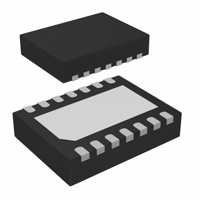
- Part No.:
- MP2611GL-P
- Manufacturer:
- Monolithic Power Systems Inc.
- Category:
- Battery Chargers
- Package:
- 14-VFDFN Exposed Pad
- Datasheet:
-
 MP2611GL-P.pdf
- Description:
- IC BATT CHG LI-ION 1CELL 14QFN
- Quantity:
- Payment:

- Shipping:

Inventory:1,602
Please send an inquiry. Send us your inquiry, and we will respond immediately.
Product details
Overview
MP2611GL-P from Monolithic Power Systems is a monolithic 1-cell Li-ion switching battery charger IC with integrated high-side P-Channel and low-side N-Channel MOSFETs, supporting dual-input (USBIN/ACIN) operation, programmable 2A charge current via external sense resistor RS1, ±0.5% battery voltage regulation accuracy, and full thermal/NTC/timer/safety protection. It targets compact portable devices requiring USB 2.0/3.0-compliant input current limiting and high-efficiency CC/CV charging.
For engineers reviewing the MP2611GL-P datasheet, MP2611GL-P pinout, MP2611GL-P application, or MP2611GL-P equivalent, this page delivers verified technical context, exact pin functions, real-world charge profile behavior, validated alternative options, and supply-chain support details - all grounded in the official MP2611 Rev. 1.12 datasheet and MPS application documentation.
Technical Context
The MP2611GL-P implements a synchronous buck topology with internal 130mΩ high-side PFET and 200mΩ low-side NFET, enabling up to 100% duty cycle for low VIN–VBATT headroom (≥200mV). Its dual-input architecture uses ACIN as primary power source and automatically falls back to USBIN when ACIN drops below 3.75V UVLO, with independent current-limit programming via RILIM on USBM pin.
Charge control employs two closed-loop regulators: one for constant-current (CC) mode using CSP–BATT sense voltage feedback (100mV threshold), and another for constant-voltage (CV) mode regulating VBATT to 4.2V ±0.5%. Status monitoring includes open-drain STAT1/STAT2 outputs, NTC thermistor window comparator (32%–74% VREF33), and internal 3-hour safety timer set by CTMR capacitor.
Key Specifications
| Parameter | Value and Actual Design Meaning |
|---|---|
| Input Voltage Range | 4.5V–6V for both ACIN and USBIN inputs - ensures compatibility with standard 5V USB and wall adapters while maintaining regulation margin. |
| Max Charge Current | 2A programmable via RS1 = 50mΩ - enables fast charging of 1-cell Li-ion packs without external current-setting DAC or op-amp. |
| Battery Voltage Accuracy | ±0.5% at 4.2V - guarantees tight CV termination to prevent overcharge and maximize cycle life per JEITA guidelines. |
| USB Input Current Limit | 500mA or 900mA selectable via RILIM (82.5kΩ or 45.3kΩ) - satisfies USB 2.0 and USB 3.0 host port compliance requirements. |
| Switching Frequency | 1.5MHz fixed - allows use of small 2.2µH inductors and ceramic output capacitors for space-constrained PCB layouts. |
| Thermal Shutdown Threshold | 150°C with 20°C hysteresis - protects die during sustained high-power operation and enables safe recovery at 130°C. |
| NTC Monitoring Range | 0°C to 50°C via NCP18XH103 thermistor - provides JEITA-compliant temperature-based charge enable/disable control. |
Pinout & Package
MP2611GL-P is housed in a thermally enhanced 3mm × 4mm QFN-14 package with exposed thermal pad on underside for efficient heat dissipation in high-current charging applications.
| Pin/Terminal | Circuit Role | Design Meaning |
|---|---|---|
| 1 ACIN | Primary adapter input | Accepts 4.5–6V AC adapter supply; triggers automatic priority selection over USBIN when >3.75V UVLO threshold. |
| 2 PGND | Power ground reference | Low-impedance return path for switching currents; must be routed outside SW-to-input loop to avoid noise coupling into analog circuitry. |
| 3 SW | Switch node output | Drives external inductor; connects directly to drain of internal high-side PFET and source of low-side NFET in synchronous buck stage. |
| 4 USBIN | Secondary USB input | Enables fallback charging from USB ports; supports programmable 500/900mA input current limit via USBM pin. |
| 5 AGND | Analog ground reference | Reference for VREF33, NTC, TMR, and sensing circuits; must be star-connected to PGND at single point to minimize offset errors. |
| 6 VREF33 | Internal 3.3V LDO output | Provides stable bias for external NTC divider and pull-ups for STAT1/STAT2; load-regulated to ±0.2V across 0–20mA. |
| 7 USBM | USB current limit set | Resistor-to-AGND sets IUSB_LIM per equation IUSB_LIM = 37000/RILIM (mA); enables precise USB 2.0/3.0 compliance. |
| 8 BATT | Battery positive terminal | Direct connection to Li-ion cell anode; used with CSP to measure charge current via RS1 sense resistor. |
| 9 CSP | Current sense positive | High-side current sense input; forms differential pair with BATT to detect 100mV across RS1 for accurate ICC regulation. |
| 10 EN | Enable control input | Active-high logic control (VIH = 1.2V, VIL = 0.8V); disables all switching and reduces quiescent current to 0.2μA when pulled low. |
| 11 STAT1 / 12 STAT2 | Open-drain status indicators | Two-pin encoding for 5 states: Charging (L/L), End-of-Charge (H/L), Fault (H/L + thermal/timer/NTC), No Input (H/H), Disabled (H/H). |
| 13 NTC | Thermistor interface | Connects to NTC thermistor and VREF33 divider; monitors battery temperature via window comparator (32–74% VREF33). |
| 14 TMR | Safety timer capacitor | External CTMR sets trickle time (30 min/0.1μF) and total charge time (3 hr/0.1μF); grounding disables timer. |
Key Features
| Feature | Design Value |
|---|---|
| Dual-input automatic priority selection | ACIN >3.75V forces primary operation; seamless USBIN fallback eliminates need for external power-path controllers. |
| Integrated synchronous power switches | 130mΩ P-FET + 200mΩ N-FET eliminate external Schottky diode, improving efficiency by ~5% and reducing BOM count. |
| Programmable USB input current limit | 500mA/900mA selection via single resistor on USBM pin - meets USB-IF specification without firmware or digital configuration. |
| Accurate 2A charge current regulation | ±1% ICC accuracy over temperature and input range using 100mV CSP–BATT sense threshold and internal gain compensation. |
| JEITA-compliant NTC monitoring | Hardware-based 0°C–50°C window detection with auto-charge suspend/resume - no MCU intervention required for thermal safety. |
| 100% duty-cycle capability | Maintains regulation down to VIN–VBATT = 200mV using high-side PFET architecture - critical for low-headroom USB charging. |
Applications
| Smartphones | Portable Media Players |
|---|---|
|
Use Scenario: Compact handheld device with dual-input charging (USB-C and wall adapter), requiring fast 2A Li-ion charge under strict thermal and JEITA constraints. IC Role / Device Role / Timing Role: Primary battery management IC handling CC/CV charge sequencing, input source arbitration, and real-time NTC/thermal/fault monitoring. Use Value: Enables full 2A charging from 5V USB sources with <200mV dropout, eliminating need for external reverse-blocking FET or discrete current-sense amplifiers. |
Use Scenario: Battery-powered audio/video player with USB 2.0 host charging and embedded thermistor for battery safety certification. IC Role / Device Role / Timing Role: Standalone switching charger managing trickle→CC→CV transitions, USB current limiting, and automatic recharge at 4.0V. Use Value: Reduces bill-of-materials by integrating power switches, reference LDO, timer, and NTC comparator - cuts PCB area by ≥30% vs. discrete solutions. |
| Tablets | Bluetooth Headsets |
|
Use Scenario: Mid-size tablet with 3000–5000mAh Li-ion battery needing efficient 2A charging and robust overtemperature protection during extended use. IC Role / Device Role / Timing Role: High-current battery charger IC providing regulated 4.2V CV output, cycle-by-cycle OCP, and thermal shutdown at 150°C. Use Value: Delivers >85% peak efficiency across 3.7–4.2V battery range and maintains safe operation even during simultaneous charging and system load. |
Use Scenario: Small-form-factor wireless headset with space-limited PCB, requiring minimal external components for USB-micro charging and battery health monitoring. IC Role / Device Role / Timing Role: Integrated charger managing low-quiescent (20μA) standby, 500mA USB2.0 input limit, and auto-recharge at 4.0V. Use Value: Eliminates need for separate LDO, timer IC, and thermistor ADC - simplifies layout and reduces component count to just RS1, RILIM, CTMR, and NTC. |
Equivalent & Alternatives
The following parts are listed as comparable options for similar single-cell Li-ion switching charger applications.
| Alternative Part | Technical Difference | Application Difference | Selection Advice |
|---|---|---|---|
| BQ24075RGTR | Linear charger (not switching); max 1.5A charge current; no integrated power FETs; requires external MOSFET for reverse blocking. | Limited to low-power applications (<1.5W dissipation); unsuitable for 2A charging due to thermal constraints; lacks USB current limit programming. | Select only if board space permits larger thermal solution and input voltage is tightly regulated near 4.5V. |
| SP6648EK-L/TR | Switching charger with 1.5A max current; no dual-input support; fixed 500mA USB limit; no NTC interface or thermal shutdown. | Requires external USB current limiting circuitry and separate thermistor ADC; lacks auto-recharge and safety timer features. | Choose only for cost-sensitive designs where 1.5A charge rate suffices and thermal monitoring is handled externally. |
Compared with BQ24075RGTR and SP6648EK-L/TR, MP2611GL-P uniquely integrates dual-input arbitration, 2A synchronous switching, hardware NTC window detection, and programmable USB current limits - delivering higher efficiency, smaller footprint, and full JEITA compliance without external support components.
Availability
MP2611GL-P is available at Aetrix Electronics and suitable for smartphones, portable media players, tablets, and Bluetooth headsets requiring stable component supply, long-term lifecycle support, and RoHS-compliant packaging.
Supply support for MP2611GL-P includes scheduled delivery planning, volume procurement assistance, BOM continuity management, traceable sourcing, and lifecycle availability coordination for OEM customers, industrial embedded developers, connected-device designers, and electronics production programs.
Manufacturer
Monolithic Power Systems (MPS) is a fabless semiconductor company specializing in high-performance analog and power ICs, with core expertise in DC/DC conversion, battery management, and motor control.
The MP2611GL-P belongs to MPS's battery charging product line, designed specifically for space-constrained portable electronics requiring high-efficiency, dual-input, and JEITA-compliant Li-ion charging with minimal external components.
FAQ
What is the minimum input-to-battery voltage difference required for regulation?
The MP2611GL-P maintains regulation with as little as 200mV headroom (VIN – VBATT ≥ 200mV) due to its high-side P-Channel MOSFET architecture and 100% duty-cycle capability - critical for maintaining charge current near end-of-charge when VBATT approaches 4.2V.
How does the MP2611GL-P handle simultaneous ACIN and USBIN presence?
When both ACIN and USBIN are present, the MP2611GL-P automatically selects ACIN as the primary power source and disables USBIN path via internal FET control. The datasheet explicitly advises against this condition due to potential cross-conduction risk, so system design must ensure only one input is active at a time.
Can the safety timer be disabled, and how?
Yes, the internal safety timer can be fully disabled by connecting the TMR pin directly to AGND. When grounded, the timer circuit is bypassed and no time-out fault will occur - useful in applications where charge duration is managed externally or where continuous trickle charge is required.
What is the function of the VREF33 pin beyond powering STAT pull-ups?
VREF33 serves as the precision 3.3V reference for the internal NTC window comparator and provides regulated bias for external thermistor dividers. Its ±0.2V load regulation over 0–20mA ensures stable NTC voltage thresholds across varying sensor loading conditions.
Does the MP2611GL-P support battery voltage monitoring during system operation?
No - the MP2611GL-P does not provide a dedicated battery voltage readback output. It regulates VBATT to 4.2V ±0.5% but lacks an analog monitor pin or I²C interface; external ADC measurement of BATT is required for telemetry.
How is USB input current limit accuracy affected by input voltage variation?
USB input current limit accuracy remains within ±5% across the full 4.5–6V USBIN range, as confirmed by Figure 6 in the datasheet. This stability is achieved through internal current-mode regulation and trimmed reference circuitry, ensuring reliable USB 2.0/3.0 compliance regardless of adapter tolerance.
What happens to charge current when transitioning from USB to ACIN input during charging?
Upon ACIN rising above 3.75V UVLO, the MP2611GL-P seamlessly switches power source and reverts to CC regulation based on RS1 - restoring full 2A charge current if previously limited by USB input current setting. No restart or interruption occurs.
MP2611GL-P Specifications
- Product attributes
- Attribute value
- Manufacturer:
- Monolithic Power Systems Inc.
- Series:
- -
- Package/Case:
- 14-VFDFN Exposed Pad
- Packaging:
- Tape & Reel (TR)
- Product Status:
- Active
- Battery Chemistry:
- Lithium Ion
- Number of Cells:
- 1
- Current - Charging:
- Constant - Programmable
- Programmable Features:
- Timer
- Fault Protection:
- Over Current, Over Temperature
- Charge Current - Max:
- 2A
- Battery Pack Voltage:
- 4.2V
- Voltage - Supply (Max):
- 6V
- Interface:
- USB
- Operating Temperature:
- -40°C ~ 125°C (TJ)
- Grade:
- -
- Qualification:
- -
- Mounting Type:
- Surface Mount
- Supplier Device Package:
- 14-QFN (3x4)
MP2611GL-P FAQ
1.How can I place an order for MP2611GL-P through Aetrix?
Please submit a Request for Quotation (RFQ) for MP2611GL-P on Aetrix. Our sales agent will provide a competitive quotation and guide you through the order confirmation once you accept the terms.
2.Are the price and stock information for MP2611GL-P reliable?
The price and inventory of MP2611GL-P are updated periodically and may fluctuate due to market conditions. Stock and pricing data are typically refreshed every 24 hours. Quotation validity for MP2611GL-P is usually 5 days.
3.What payment methods are accepted for MP2611GL-P?
We accept Wire Transfer, PayPal, Credit Card, Western Union, MoneyGram, and Escrow for MP2611GL-P transactions.
Note: Certain payment methods may incur a processing fee.
4.How is shipping managed for MP2611GL-P?
MP2611GL-P orders can be shipped via leading logistics carriers, including DHL, UPS, FedEx, TNT, or Registered Mail.
Once your MP2611GL-P order is processed, you will receive an email with the shipment details and tracking number.
Note: Tracking information may take up to 24 hours to appear. Express delivery typically takes 3–5 business days.
5.How can I obtain technical support or documentation for MP2611GL-P?
For technical support, including MP2611GL-P datasheets, pinout diagrams, or application guidance, please contact our engineering support team. They can provide detailed documentation and assistance for your MP2611GL-P requirements.
6.How does Aetrix verify that MP2611GL-P is sourced from the original manufacturer or authorized distributors?
All MP2611GL-P products on Aetrix are procured from qualified distributors and authorized channels. Our dedicated quality assurance team conducts strict verification, including traceability checks and, if necessary, third-party testing. This ensures that MP2611GL-P meets industry standards.
7.What is the process for return or replacement of MP2611GL-P?
All MP2611GL-P units undergo pre-shipment inspection (PSI). If there is an issue with MP2611GL-P, returns or replacements are accepted under the following conditions:
1.Quantity discrepancies, incorrect items, or visible external defects (such as breakage or corrosion), acknowledged by Aetrix.
2.The issue is reported within 90 days of delivery.
3.The MP2611GL-P part is unused and in its original packaging.
Return procedure for MP2611GL-P:
1.Submit a request within 90 days.
2.Obtain a Return Material Authorization (RMA) from Aetrix.
MP2611GL-P Tags

-
BQ21040DBVR
Texas Instruments

-
MCP73812T-420I/OT
Microchip Technology
-
MCP73831T-2ACI/OT
Microchip Technology
-
MCP73832T-2ACI/OT
Microchip Technology
-
MCP73831T-2DCI/OT
Microchip Technology
-
MCP73832T-2DCI/OT
Microchip Technology
-
MCP73831T-2ATI/OT
Microchip Technology
-
MCP73832T-2ATI/OT
Microchip Technology
-
MCP73831T-5ACI/OT
Microchip Technology

-
MCP73832T-2ACI/MC
Microchip Technology
-
MCP73831T-2ACI/MC
Microchip Technology
-
MCP73831T-2ATI/MC
Microchip Technology
Tech Hub

Operational amplifier guide covering op amp basics, feedback, ideal vs real op amps, common configurations, buffer circuits, offset, bias current, gain-bandwidth, slew rate, rail-to-rail limits and sel…

Jumper cables guide covering safe connection order, red and black clamp placement, final ground connection, cable gauge, length, clamp quality, copper vs CCA cables, jump starter comparison and battery…

LDO regulator guide covering low dropout voltage, power dissipation, thermal design, PSRR, output noise, capacitor stability, adjustable LDO circuits, LDO vs buck converter and datasheet selection chec…

Conditional Access Module guide covering CAM meaning, CI/CI+ interface, smart card authorization, DVB security workflow, TV and set-top box compatibility, internal electronics, ESD protection, connecto…

Guide to electronic component obsolescence covering EOL risk, PCN/PDN notices, last-time buy planning, replacement options, form-fit-function validation, counterfeit risk and BOM lifecycle management.

18650 battery guide covering lithium-ion cell basics, 3.6V/3.7V voltage, 4.2V charging, mAh and Wh capacity, protected cells, chargers, BMS, series-parallel packs, holders, welding and sourcing checks.…

Hall effect sensor guide covering working principle, linear and digital sensors, Arduino circuits, current sensing, speed detection, automotive applications, A3144 examples, signal filtering and datash…

Product Change Notification guide for electronic components, covering PCN meaning, PCN vs PDN/EOL, common change types, risk levels, form-fit-function review, engineering validation, BOM control, LTB/L…

A practical guide to blend door actuators, covering HVAC function, symptoms, location, AC and heater issues, reset and calibration, replacement cost, electrical diagnosis, compatibility checks, and rep…

Engineering guide to Raspberry Pi alternatives, covering chip-level differences, Orange Pi, ROCK, Jetson, Banana Pi, NanoPi, Compute Module, Pico, GPIO, camera, HAT compatibility, and replacement risks…


