
 My Inquiry
 My Account


Monolithic Power Systems Inc. MP2617BGL-P
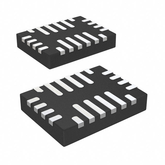
- Part No.:
- MP2617BGL-P
- Manufacturer:
- Monolithic Power Systems Inc.
- Category:
- Battery Chargers
- Package:
- 20-PowerTFQFN
- Datasheet:
-
 MP2617BGL-P.pdf
- Description:
- IC BATT CHG LI-ION 1CELL 20QFN
- Quantity:
- Payment:

- Shipping:

Inventory:500
Please send an inquiry. Send us your inquiry, and we will respond immediately.
Product details
Overview
MP2617BGL-P from Monolithic Power Systems is a monolithic 3A synchronous buck switching charger IC with integrated NVDC (Narrow Voltage DC) power path management for single-cell Li-ion batteries. It delivers regulated SYS output voltage (4.08–4.4V programmable), supports dual-input USB/DC adapter (4–10V), and implements five independent control loops including input current limit (up to 3A), constant charge current (up to 3.025A), and thermal fold-back. It enables immediate system operation with deeply discharged or absent batteries in portable tablets and smartphones.
For engineers reviewing the MP2617BGL-P datasheet, MP2617BGL-P pinout, MP2617BGL-P application, or MP2617BGL-P equivalent, key selection considerations include its 4.2V fixed battery full-charge voltage, QFN-20 (3mm×4mm) package with exposed thermal pad, smart power path priority logic (system load > battery charge), and integrated ideal diode function enabling battery-to-system supplemental power during input overload or removal.
Technical Context
The MP2617BGL-P integrates a 1.6MHz fixed-frequency synchronous buck converter with internal high-side (130mΩ) and low-side (100mΩ) NMOS switches, eliminating external MOSFETs, blocking diodes, and sense resistors. Its NVDC architecture decouples SYS rail regulation from battery charging via independent feedback paths: SYSFB sets system output voltage, while ISET programs charge current and ILIM configures input current limit.
Five closed-loop controls operate concurrently: input current limit (programmable via M0/M1 pins or ILIM resistor), input voltage clamp (via VLIM pin), constant-current/constant-voltage battery charge (with 4.2V termination), battery terminal voltage regulation, and on-die thermal fold-back at 120°C. The device uses fixed off-time control for high duty-cycle operation near VIN ≈ VSYS and includes built-in trickle charge, NTC monitoring, and programmable safety timer.
Key Specifications
| Parameter | Value and Actual Design Meaning |
|---|---|
| Input Voltage Range | 4.0V to 10.0V - Supports USB 2.0/3.0 and wide-range DC adapters without external LDO or overvoltage protection. |
| Max Charge Current | 3.025A @ RISET = 760Ω - Enables fast charging of 2000–3000mAh Li-ion cells within thermal limits. |
| Battery Full Voltage | 4.20V ±21mV - Precise termination threshold optimized for standard single-cell Li-ion chemistry. |
| Switching Frequency | 1.6MHz (typ.) - Allows compact 1.2µH inductor and reduces EMI filtering requirements. |
| Power Path Priority | System load satisfied before battery charge - Ensures uninterrupted operation even when input power is marginal or battery is deeply discharged. |
| Thermal Regulation | Fold-back activation at 120°C, shutdown at 150°C - On-chip thermal sensing eliminates need for external thermistors for basic thermal safety. |
| Package | QFN-20 (3mm × 4mm, 0.5mm pitch) with exposed thermal pad - Optimized for space-constrained portable PCBs and efficient heat dissipation (θJA = 48°C/W). |
Pinout & Package
MP2617BGL-P is housed in a thermally enhanced QFN-20 package (3mm × 4mm, 0.5mm pitch) with an exposed thermal pad on the bottom for PCB-level heat sinking. Pin numbering follows standard top-view orientation with Pin 1 at top-left corner.
| Pin/Terminal | Circuit Role | Design Meaning |
|---|---|---|
| 1 BST | Bootstrap supply | Connects external capacitor between BST and SW to generate gate drive voltage > VIN for high-side NMOS switch. |
| 3 IN | Main power input | Accepts 4–10V from USB or DC adapter; feeds buck converter and enables ACOK status signal. |
| 2,4 SW | Switch node | Drives external inductor; connects to BST capacitor and internal high/low-side NMOS switches. |
| 5 PGND | Power ground | High-current return path for inductor and internal power switches; separate from AGND to reduce noise coupling. |
| 6 EN | Enable control | Active-low logic input; pulls device into ultra-low quiescent state (<5µA) when held high. |
| 7 M0 / 8 M1 | Input current mode select | Logic pair selects USB2.0 (450mA), USB3.0 (825mA), programmable (RILIM), or default (2A) input limit. |
| 9 CHGOK | Charge status indicator | Open-drain output pulled low during active charging; high (via external pull-up) indicates full-charge completion. |
| 10 ACOK | Input power presence | Open-drain output pulled low when valid input (IN > UVLO + 280mV above BATT) is detected. |
| 12 SYSFB | System output voltage feedback | Resistor divider from SYS to AGND programs VSYS from 4.08V to 4.4V; floating disables programming. |
| 13 SYS | Regulated system output | Delivers up to 3A to system load; dynamically tracks battery voltage (VBATT + 200mV) above 3.4V or holds 3.6V below. |
| 14 BATT | Battery terminal | Connects directly to Li-ion cell anode; internal 40mΩ ideal diode enables battery-to-SYS power supplement. |
| 15 ISET | Charge current programming | Resistor to AGND sets ICC (e.g., 760Ω → 3.025A); floating disables charging. |
| 16 NTC | Battery temperature monitor | Accepts NCP18XH103F thermistor network; triggers charge suspension outside 0°C–50°C range. |
| 17 ILIM | Adapter input current limit | Resistor to AGND programs input current limit (e.g., 22.47kΩ → 2A for MP2617B); USB mode overrides this setting. |
| 19 VLIM | Input voltage clamp reference | Resistor divider from IN to AGND sets input clamp voltage (e.g., 1.52V threshold) to protect weak adapters. |
Key Features
| Feature | Design Value |
|---|---|
| Integrated power switches | Internal 130mΩ high-side and 100mΩ low-side NMOS eliminate external FETs, reducing BOM count and layout area. |
| NVDC power path | Independent regulation of SYS rail and battery charge enables system boot with dead battery and seamless transition between input/battery power sources. |
| Five concurrent control loops | Simultaneous input current, input voltage, constant-current, constant-voltage, and thermal regulation ensure robust operation under dynamic load and source conditions. |
| Programmable safety timer | TMR pin connection to AGND disables internal timer; 0.1µF capacitor enables 6.5-hour total charge timeout to prevent overcharge of defective cells. |
| USB-compliant input limiting | Hardware-selectable 450mA (USB2.0) or 825mA (USB3.0) input current limits meet specification compliance without firmware intervention. |
| Trickle-to-CC-CV charge profile | Automatically initiates 10% ICC trickle charge below 3.0V, transitions to full CC above threshold, and terminates at 4.2V with 85mV hysteresis for recharge. |
Applications
| Tablet PC | Smartphone |
|---|---|
|
Use Scenario: Dual-power-source tablet requiring instant-on capability with degraded or missing battery. IC Role / Device Role / Timing Role: Primary switching charger and NVDC power path manager regulating SYS rail and charging Li-ion cell independently. Use Value: Enables system operation at 3.6V even with 0V battery, while simultaneously charging at up to 3A using available input power-no external ideal diode or OR-ing controller needed. |
Use Scenario: Compact smartphone supporting both USB-C PD and legacy USB charging with thermal-aware battery management. IC Role / Device Role / Timing Role: Integrated buck charger with real-time input current limiting, battery temperature monitoring, and adaptive SYS voltage tracking. Use Value: Maintains USB2.0/3.0 compliance via hardware M0/M1 pin configuration, prevents overheating via 120°C thermal fold-back, and extends cycle life with precise 4.2V termination and 85mV recharge hysteresis. |
| E-Book Reader | Portable Media Player |
|
Use Scenario: Low-power e-reader with long standby time and infrequent but rapid recharge via micro-USB. IC Role / Device Role / Timing Role: Energy-efficient charging controller managing trickle, CC, and CV phases with programmable timer and NTC supervision. Use Value: Reduces standby current to <5µA when disabled (EN high), ensures safe charging across temperature extremes (0°C–50°C), and avoids overcharge via 6.5-hour safety timer. |
Use Scenario: Portable media player with variable system load (audio decode, display backlight) and shared USB port for data + power. IC Role / Device Role / Timing Role: Smart power distributor prioritizing system load over battery charge during peak demand, then resuming charge when load drops. Use Value: Prevents brownouts during audio playback by dynamically throttling charge current to maintain stable 4.2V SYS rail, while still delivering up to 3A average charge when idle. |
Equivalent & Alternatives
The following parts are listed as comparable options for similar single-cell Li-ion switching charger applications.
| Alternative Part | Technical Difference | Application Difference | Selection Advice |
|---|---|---|---|
| BQ25611DRTWR | 4.2V battery full voltage same; supports I²C interface (MP2617BGL-P is pin-programmed only); lower max input voltage (13.5V vs. 10V); higher quiescent current (15µA vs. 5µA) | Requires MCU firmware for configuration; better suited for systems needing dynamic parameter updates or telemetry | Select if I²C configurability and higher input voltage margin outweigh need for simpler pin-strapping and lower IQ. |
| IP2326 | Fixed 4.2V termination; no SYSFB programmability (VSYS fixed at 4.2V); no input voltage clamp (VLIM) or NTC monitoring; smaller QFN-16 package | Lacks NVDC power path flexibility and thermal/battery safety features; targets cost-sensitive, low-feature applications | Select only for ultra-low-cost designs where SYS voltage adaptability, input protection, and comprehensive battery supervision are not required. |
Compared with BQ25611DRTWR and IP2326, MP2617BGL-P offers superior integration for pin-strapped, thermally constrained portable devices-delivering programmable SYS voltage, input voltage clamping, and full five-loop regulation without MCU dependency or feature trade-offs.
Availability
MP2617BGL-P is available at Aetrix Electronics and suitable for tablet PC, smartphone, e-book reader, and portable media player designs requiring stable component supply, consistent thermal performance, and long-term lifecycle support in high-volume consumer electronics production.
Supply support for MP2617BGL-P includes scheduled delivery planning, volume procurement assistance, BOM continuity management, traceable sourcing, and lifecycle availability coordination for OEM customers, industrial embedded developers, connected-device designers, and electronics production programs.
Manufacturer
Monolithic Power Systems (MPS) is a fabless semiconductor company specializing in high-performance analog and power ICs, with core expertise in DC-DC conversion, battery management, and motor control solutions.
The MP2617 series belongs to MPS's portable battery charger product line, designed specifically for space-constrained, dual-input (USB + adapter) consumer devices requiring robust NVDC power path management and high integration density.
FAQ
What is the difference between MP2617A and MP2617B?
The primary distinction lies in battery full-charge voltage: MP2617A terminates at 4.35V, while MP2617B uses 4.2V-making MP2617B compatible with standard Li-ion cells without overvoltage risk. Additionally, MP2617B's programmable SYS voltage range is 4.08V–4.4V versus MP2617A's 4.22V–4.63V, aligning with typical system rail requirements.
How does the NVDC power path manage system load priority?
When input current reaches its programmed limit, the MP2617BGL-P first satisfies the system load demand on the SYS rail. Only residual current is allocated to battery charging. If system load exceeds input capacity, the internal 40mΩ BATT-to-SYS MOSFET turns on, allowing battery to supplement power-ensuring uninterrupted SYS operation without brownout.
Can MP2617BGL-P operate without an external inductor?
No. The device requires an external 1.2µH power inductor connected between SW and the input/output filter capacitors. The internal synchronous buck controller relies on this inductor for energy storage and transfer; omission would prevent regulation and likely cause immediate fault or damage.
What happens if the NTC thermistor is disconnected?
If the NTC pin is left floating or open-circuited, the device interprets it as an out-of-range temperature condition and suspends charging. This is a safety lockout per JEITA guidelines-charging resumes only when a valid thermistor network (e.g., NCP18XH103F) is reconnected and reports temperature within 0°C–50°C.
Is the MP2617BGL-P RoHS and halogen-free compliant?
Yes. MP2617BGL-P is lead-free, halogen-free, and fully compliant with the EU RoHS directive. All packaging materials and die attach compounds meet MPS's green manufacturing standards, as verified and published on the Monolithic Power Systems quality assurance website.
How is input current limit set in USB mode?
In USB mode, the MP2617BGL-P ignores the ILIM resistor and instead uses internal logic: M0/M1 pin states determine fixed limits-Low/Low = 450mA (USB2.0), Low/High = 825mA (USB3.0). When both pins float (default), it operates at 2A, but this setting is invalid for USB compliance and intended for DC adapter use only.
Does MP2617BGL-P support reverse current blocking from SYS to IN?
Yes. When VIN = 0V and SYS = 4.5V, the device blocks reverse current with leakage <0.2µA-achieved via internal high-side NMOS gate control. This prevents battery or SYS rail discharge back into a disconnected or failed input source, protecting both power sources.
MP2617BGL-P Specifications
- Product attributes
- Attribute value
- Manufacturer:
- Monolithic Power Systems Inc.
- Series:
- -
- Package/Case:
- 20-PowerTFQFN
- Packaging:
- Tape & Reel (TR)
- Product Status:
- Active
- Battery Chemistry:
- Lithium Ion
- Number of Cells:
- 1
- Current - Charging:
- Constant - Programmable
- Programmable Features:
- Timer
- Fault Protection:
- Over Temperature
- Charge Current - Max:
- -
- Battery Pack Voltage:
- 4.2V
- Voltage - Supply (Max):
- 10V
- Interface:
- USB
- Operating Temperature:
- -40°C ~ 125°C (TJ)
- Grade:
- -
- Qualification:
- -
- Mounting Type:
- Surface Mount
- Supplier Device Package:
- 20-QFN (3x4)
MP2617BGL-P FAQ
1.How can I place an order for MP2617BGL-P through Aetrix?
Please submit a Request for Quotation (RFQ) for MP2617BGL-P on Aetrix. Our sales agent will provide a competitive quotation and guide you through the order confirmation once you accept the terms.
2.Are the price and stock information for MP2617BGL-P reliable?
The price and inventory of MP2617BGL-P are updated periodically and may fluctuate due to market conditions. Stock and pricing data are typically refreshed every 24 hours. Quotation validity for MP2617BGL-P is usually 5 days.
3.What payment methods are accepted for MP2617BGL-P?
We accept Wire Transfer, PayPal, Credit Card, Western Union, MoneyGram, and Escrow for MP2617BGL-P transactions.
Note: Certain payment methods may incur a processing fee.
4.How is shipping managed for MP2617BGL-P?
MP2617BGL-P orders can be shipped via leading logistics carriers, including DHL, UPS, FedEx, TNT, or Registered Mail.
Once your MP2617BGL-P order is processed, you will receive an email with the shipment details and tracking number.
Note: Tracking information may take up to 24 hours to appear. Express delivery typically takes 3–5 business days.
5.How can I obtain technical support or documentation for MP2617BGL-P?
For technical support, including MP2617BGL-P datasheets, pinout diagrams, or application guidance, please contact our engineering support team. They can provide detailed documentation and assistance for your MP2617BGL-P requirements.
6.How does Aetrix verify that MP2617BGL-P is sourced from the original manufacturer or authorized distributors?
All MP2617BGL-P products on Aetrix are procured from qualified distributors and authorized channels. Our dedicated quality assurance team conducts strict verification, including traceability checks and, if necessary, third-party testing. This ensures that MP2617BGL-P meets industry standards.
7.What is the process for return or replacement of MP2617BGL-P?
All MP2617BGL-P units undergo pre-shipment inspection (PSI). If there is an issue with MP2617BGL-P, returns or replacements are accepted under the following conditions:
1.Quantity discrepancies, incorrect items, or visible external defects (such as breakage or corrosion), acknowledged by Aetrix.
2.The issue is reported within 90 days of delivery.
3.The MP2617BGL-P part is unused and in its original packaging.
Return procedure for MP2617BGL-P:
1.Submit a request within 90 days.
2.Obtain a Return Material Authorization (RMA) from Aetrix.
MP2617BGL-P Tags

-
BQ21040DBVR
Texas Instruments

-
MCP73812T-420I/OT
Microchip Technology
-
MCP73831T-2ACI/OT
Microchip Technology
-
MCP73832T-2ACI/OT
Microchip Technology
-
MCP73831T-2DCI/OT
Microchip Technology
-
MCP73832T-2DCI/OT
Microchip Technology
-
MCP73831T-2ATI/OT
Microchip Technology
-
MCP73832T-2ATI/OT
Microchip Technology
-
MCP73831T-5ACI/OT
Microchip Technology

-
MCP73832T-2ACI/MC
Microchip Technology
-
MCP73831T-2ACI/MC
Microchip Technology
-
MCP73831T-2ATI/MC
Microchip Technology
Tech Hub

Operational amplifier guide covering op amp basics, feedback, ideal vs real op amps, common configurations, buffer circuits, offset, bias current, gain-bandwidth, slew rate, rail-to-rail limits and sel…

Jumper cables guide covering safe connection order, red and black clamp placement, final ground connection, cable gauge, length, clamp quality, copper vs CCA cables, jump starter comparison and battery…

LDO regulator guide covering low dropout voltage, power dissipation, thermal design, PSRR, output noise, capacitor stability, adjustable LDO circuits, LDO vs buck converter and datasheet selection chec…

Conditional Access Module guide covering CAM meaning, CI/CI+ interface, smart card authorization, DVB security workflow, TV and set-top box compatibility, internal electronics, ESD protection, connecto…

Guide to electronic component obsolescence covering EOL risk, PCN/PDN notices, last-time buy planning, replacement options, form-fit-function validation, counterfeit risk and BOM lifecycle management.

18650 battery guide covering lithium-ion cell basics, 3.6V/3.7V voltage, 4.2V charging, mAh and Wh capacity, protected cells, chargers, BMS, series-parallel packs, holders, welding and sourcing checks.…

Hall effect sensor guide covering working principle, linear and digital sensors, Arduino circuits, current sensing, speed detection, automotive applications, A3144 examples, signal filtering and datash…

Product Change Notification guide for electronic components, covering PCN meaning, PCN vs PDN/EOL, common change types, risk levels, form-fit-function review, engineering validation, BOM control, LTB/L…

A practical guide to blend door actuators, covering HVAC function, symptoms, location, AC and heater issues, reset and calibration, replacement cost, electrical diagnosis, compatibility checks, and rep…

Engineering guide to Raspberry Pi alternatives, covering chip-level differences, Orange Pi, ROCK, Jetson, Banana Pi, NanoPi, Compute Module, Pico, GPIO, camera, HAT compatibility, and replacement risks…


