
 My Inquiry
 My Account


Monolithic Power Systems Inc. MP2667GG-0000-Z
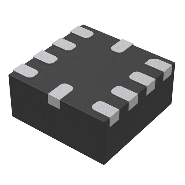
- Part No.:
- MP2667GG-0000-Z
- Manufacturer:
- Monolithic Power Systems Inc.
- Category:
- Battery Chargers
- Package:
- 10-TFQFN
- Datasheet:
-
 MP2667GG-0000-Z.pdf
- Description:
- 5V USB, 1000MA, I2C-CONTROLLED L
- Quantity:
- Payment:

- Shipping:

Inventory:3,975
Please send an inquiry. Send us your inquiry, and we will respond immediately.
Product details
Overview
MP2667GG-0000-Z from Monolithic Power Systems is a single-cell Li-ion/Li-polymer linear battery charger with integrated power path management, I²C programmability, and dual FET architecture (300 mΩ IN→SYS LDO + 100 mΩ BATT→SYS switch). It delivers up to 1000 mA charge current, supports 4.35–5.5 V USB input, regulates system voltage to 5.00 V ±150 mV, and enables simultaneous system powering and battery charging in space-constrained wearables.
For engineers reviewing the MP2667GG-0000-Z datasheet, MP2667GG-0000-Z pinout, MP2667GG-0000-Z application, or MP2667GG-0000-Z equivalent, key selection considerations include I²C-configurable charge parameters (VBATT_REG: 3.60–4.545 V, ICC: 26–1049 mA), thermal regulation at 120°C, programmable input current limit (77–993 mA), and battery UVLO threshold (2.4–3.1 V).
Technical Context
The MP2667 implements a direct power path architecture with independent control of the IN→SYS LDO FET and BATT→SYS discharge FET, enabling true system priority startup even with deeply discharged batteries. Its charge algorithm executes three phases-pre-charge (programmable 6–25 mA), constant-current fast charge (26–1049 mA), and constant-voltage regulation (±0.5% accuracy at 4.200 V)-with auto-recharge triggered at 140–370 mV below full charge.
Power path operation is governed by real-time loop arbitration: when input current or voltage falls below programmed thresholds (VIN_MIN: 3.88–5.08 V; IIN_LIM: 77–993 mA), the IC reduces charge current or engages the battery FET to supplement system load. Fault handling includes NTC-based temperature monitoring (cold/hot thresholds set as % of VIN), input OVP (6.00 V), and system short-circuit protection limiting ISYS to 1.6 A.
Key Specifications
| Parameter | Value and Actual Design Meaning |
|---|---|
| Charge Current Range | 26–1049 mA via I²C register REG02[4:0]; enables precise matching to battery capacity and thermal constraints. |
| Battery Regulation Voltage | 3.60–4.545 V programmable (REG04[7:2]); ±0.5% accuracy at 4.200 V ensures safe Li-ion full-charge termination. |
| Input Voltage Range | 4.35–5.5 V (USB-compliant); supports standard 5 V adapters while rejecting brownouts below 3.9 V UVLO. |
| System Output Voltage | 5.00 V ±150 mV (VSYS_REG); regulated independently of battery state for stable MCU/peripheral supply. |
| Thermal Regulation Threshold | 120°C (REG06[1:0] = 11); dynamically throttles charge current to prevent die overheating without shutdown. |
| Input Current Limit | 77–993 mA (I²C REG00[2:0]); prevents USB port overload and enforces compliance with host power budgets. |
| Battery UVLO Threshold | 2.4–3.1 V programmable (REG04[1:0]); configurable under-voltage cutoff prevents Li-ion over-discharge damage. |
Pinout & Package
MP2667GG-0000-Z is housed in a 10-pin QFN package (2 mm × 2 mm, 0.5 mm pitch) with exposed thermal pad. The package supports high-density layout and efficient heat dissipation in ultra-thin portable designs.
| Pin/Terminal | Circuit Role | Design Meaning |
|---|---|---|
| 1 IN | Power Input | Accepts 4.35–5.5 V USB/adapter input; requires ≥1 μF ceramic capacitor to GND for stability. |
| 2 NTC | Analog Input | Connects to NTC thermistor divider; monitors battery temperature with programmable hot/cold windows. |
| 3 INT | Open-Drain Output | Signals charge status/faults to host; pull low >8 s to disconnect battery from system (shipping mode). |
| 4 VDD | Internal Bias Supply | Powers internal logic; requires 0.1 μF decoupling capacitor; no external load permitted. |
| 5 GND | Ground Reference | Common return for all analog/digital circuits; must be low-impedance connection to thermal pad. |
| 6 SCL | I²C Clock | Bi-directional clock line; requires 10 kΩ pull-up to logic rail for standard/fast-mode I²C (≤400 kHz). |
| 7 SDA | I²C Data | Bi-directional data line; requires 10 kΩ pull-up to logic rail; supports read/write of all configuration/status registers. |
| 8,9 BATT | Battery Terminal | Connects to single-cell Li-ion anode; 100 mΩ internal FET enables controlled discharge and charge path isolation. |
| 10 SYS | System Power Output | Delivers regulated 5 V to load; separates system supply from battery voltage, enabling seamless input/battery switchover. |
Key Features
| Feature | Design Value |
|---|---|
| Integrated Power Path Architecture | Dual-FET structure (300 mΩ IN→SYS LDO + 100 mΩ BATT→SYS) enables independent system/battery control and eliminates need for external blocking diodes. |
| I²C Programmable Charging Parameters | Full configuration of VBATT_REG (3.60–4.545 V), ICC (26–1049 mA), IIN_LIM (77–993 mA), VIN_MIN (3.88–5.08 V), and safety timers via 8-bit registers. |
| Robust Battery Protection Suite | Includes programmable UVLO/OVP, NTC-based thermal monitoring, 200 μs input immunity timer, and automatic charge termination with auto-recharge. |
| Shipping Mode Disconnection | INT pin command (>8 s low pulse) disables BATT→SYS FET, reducing quiescent current to ≤5 μA for long-term storage. |
| Thermal Regulation with Hysteresis | Junction temperature regulation at 120°C (±0°C hysteresis) maintains safe operation without thermal shutdown cycles. |
Applications
| Wearable Fitness Tracker | Smart Bluetooth Headphone |
|---|---|
|
Use Scenario: Compact wearable with 150–300 mAh Li-polymer battery, charged via micro-USB port and operating continuously during activity tracking. IC Role / Device Role / Timing Role: Linear charger managing CC/CV charge profile while powering sensor/MCU subsystems directly from SYS pin; INT pin signals charge completion to host MCU. Use Value: Enables <12-hour recharge time at 500 mA while maintaining 5.00 V system rail stability during charging-critical for accurate heart-rate sensor operation. |
Use Scenario: Dual-earbud TWS system where each earpiece uses a 50–80 mAh cell and charges from a compact case with limited PCB area. IC Role / Device Role / Timing Role: Single-chip solution providing power path management to run earpiece electronics from USB input while charging battery, with shipping mode activation for factory packaging. Use Value: Reduces BOM count by eliminating discrete load switches and diodes; 2 mm × 2 mm QFN fits within tight 8 mm × 8 mm earpiece footprint. |
| Ultra-Thin Smartwatch | Wireless Sensor Node |
|
Use Scenario: Round-form-factor smartwatch with curved 300–400 mAh battery and strict height constraint (<10 mm total thickness). IC Role / Device Role / Timing Role: I²C-controlled charger regulating 4.20 V battery voltage with ±0.5% accuracy; NTC input monitors battery temperature during rapid charging in confined enclosure. Use Value: Prevents thermal runaway during 800 mA fast charge by triggering 120°C thermal regulation-ensuring safety without compromising charge speed. |
Use Scenario: Industrial wireless node powered by single-cell Li-ion, deployed in remote locations requiring multi-year battery life and field firmware updates via USB. IC Role / Device Role / Timing Role: Charger with programmable 2.8 V battery UVLO and 20-hour safety timer; INT pin asserts fault on overtemperature or NTC open-circuit. Use Value: Extends operational lifetime by preventing deep discharge damage and enabling reliable recovery after firmware update-induced power cycles. |
Equivalent & Alternatives
The following parts are listed as comparable options for similar single-cell Li-ion charger with power path applications.
| Alternative Part | Technical Difference | Application Difference | Selection Advice |
|---|---|---|---|
| BQ24296RGER | Higher max input voltage (13.5 V vs. 13 V); fixed 4.2 V battery regulation (non-programmable); no NTC input. | Lacks programmable VBATT_REG and thermal monitoring-unsuitable for applications requiring custom voltage profiles or battery temperature safety. | Select if only standard 4.2 V charging is needed and NTC monitoring is not required; verify compatibility with existing I²C register map. |
| MAX77818EWJ+T | Switching charger architecture (higher efficiency); integrates buck converter + linear charger; larger 20-pin WLP package (2.13 mm × 2.13 mm). | Higher thermal performance in high-power scenarios but introduces switching noise-requires additional EMI filtering near sensitive RF/analog circuits. | Prefer for >1 A charge currents or thermally constrained environments; avoid in noise-sensitive audio/wearable designs without added filtering. |
Compared with BQ24296RGER and MAX77818EWJ+T, MP2667GG-0000-Z uniquely balances ultra-compact size, full I²C configurability (including NTC and UVLO), and linear simplicity-making it optimal for sub-10 mm-thick wearables where board area and analog integrity outweigh raw efficiency gains.
Availability
MP2667GG-0000-Z is available at Aetrix Electronics and suitable for wearable fitness trackers, smart Bluetooth headphones, ultra-thin smartwatches, and wireless sensor nodes requiring stable component supply across design-in, prototyping, and volume production phases.
Supply support for MP2667GG-0000-Z includes scheduled delivery planning, volume procurement assistance, BOM continuity management, traceable sourcing, and lifecycle availability coordination for OEM customers, industrial embedded developers, connected-device designers, and electronics production programs.
Manufacturer
Monolithic Power Systems (MPS) is a fabless semiconductor company specializing in high-performance power management ICs, with over two decades of expertise in DC/DC converters, battery chargers, and motor drivers.
The MP2667 belongs to MPS's highly integrated linear battery charger product line, designed specifically for space-constrained portable electronics requiring robust power path management, I²C configurability, and comprehensive battery protection.
FAQ
What is the maximum allowable input voltage for MP2667GG-0000-Z, and what protection activates beyond that?
The absolute maximum input voltage is +13 V, but the device enters over-voltage protection (OVP) at 6.00 V (typical rising threshold). At this point, the IN→SYS LDO FET turns off immediately to protect internal circuitry. Recovery occurs only after input voltage drops below 5.633 V (6.00 V − 367 mV hysteresis), ensuring stable re-engagement without oscillation.
How does the MP2667 handle system power when the battery is deeply discharged or missing?
The MP2667 prioritizes system startup using its IN→SYS LDO FET. Even with a 0 V battery, the IC powers the SYS rail from the input source (4.35–5.5 V) and regulates it to 5.00 V ±150 mV. This ensures immediate MCU/peripheral operation without waiting for battery pre-charge, a critical feature for wearables requiring instant-on functionality.
Can the battery UVLO threshold be adjusted, and what is its functional range?
Yes, the battery under-voltage lockout (UVLO) threshold is fully programmable via I²C register REG04[1:0], spanning 2.4 V to 3.1 V in 0.1 V steps. At default setting (2.8 V), the hysteresis is 227 mV-meaning the FET reconnects only when battery voltage rises above 3.027 V, preventing oscillation near cutoff.
What is the role of the INT pin beyond interrupt signaling?
INT serves dual functions: (1) open-drain interrupt output for charge status/fault reporting (e.g., EOC, thermal fault), and (2) hardware-controlled battery disconnect. Pulling INT low for >8 seconds forces the BATT→SYS FET off, reducing system quiescent current to ≤5 μA-enabling true shipping mode for factory packaging and long-term storage.
Does MP2667GG-0000-Z support charging from non-USB sources, and what are the limits?
Yes-it accepts any 4.35–5.5 V DC source, including wall adapters and power banks. The input over-voltage protection triggers at 6.00 V, and absolute maximum rating is 13 V. However, sustained operation above 5.5 V violates recommended conditions and may degrade reliability or trigger OVP repeatedly.
How is thermal regulation implemented, and is it user-configurable?
Thermal regulation is implemented via an on-die temperature sensor and programmable junction threshold. Register REG06[1:0] sets TJ_REG to 120°C (default), 125°C, 130°C, or disabled. When exceeded, the IC linearly reduces charge current to maintain die temperature at the setpoint-avoiding thermal shutdown and preserving system operation.
What is the minimum external capacitance required on the IN pin, and why is placement critical?
A minimum 1 μF ceramic capacitor is required between IN and GND, placed as close as possible to pins 1 and 5. This stabilizes the input rail during transient load changes (e.g., MCU wake-up bursts) and prevents false triggering of input UVLO due to localized voltage droop at the IC's input node.
MP2667GG-0000-Z Specifications
- Product attributes
- Attribute value
- Manufacturer:
- Monolithic Power Systems Inc.
- Series:
- -
- Package/Case:
- 10-TFQFN
- Packaging:
- Tape & Reel (TR)
- Product Status:
- Active
- Battery Chemistry:
- Lithium Ion/Polymer
- Number of Cells:
- 1
- Current - Charging:
- Constant
- Programmable Features:
- Timer
- Fault Protection:
- Over Current, Over Temperature, Over Voltage, Short Circuit
- Charge Current - Max:
- 1.6A
- Battery Pack Voltage:
- 5V
- Voltage - Supply (Max):
- 5.5V
- Interface:
- I2C, USB
- Operating Temperature:
- -40°C ~ 125°C (TJ)
- Grade:
- -
- Qualification:
- -
- Mounting Type:
- Surface Mount
- Supplier Device Package:
- 10-QFN (2x2)
MP2667GG-0000-Z FAQ
1.How can I place an order for MP2667GG-0000-Z through Aetrix?
Please submit a Request for Quotation (RFQ) for MP2667GG-0000-Z on Aetrix. Our sales agent will provide a competitive quotation and guide you through the order confirmation once you accept the terms.
2.Are the price and stock information for MP2667GG-0000-Z reliable?
The price and inventory of MP2667GG-0000-Z are updated periodically and may fluctuate due to market conditions. Stock and pricing data are typically refreshed every 24 hours. Quotation validity for MP2667GG-0000-Z is usually 5 days.
3.What payment methods are accepted for MP2667GG-0000-Z?
We accept Wire Transfer, PayPal, Credit Card, Western Union, MoneyGram, and Escrow for MP2667GG-0000-Z transactions.
Note: Certain payment methods may incur a processing fee.
4.How is shipping managed for MP2667GG-0000-Z?
MP2667GG-0000-Z orders can be shipped via leading logistics carriers, including DHL, UPS, FedEx, TNT, or Registered Mail.
Once your MP2667GG-0000-Z order is processed, you will receive an email with the shipment details and tracking number.
Note: Tracking information may take up to 24 hours to appear. Express delivery typically takes 3–5 business days.
5.How can I obtain technical support or documentation for MP2667GG-0000-Z?
For technical support, including MP2667GG-0000-Z datasheets, pinout diagrams, or application guidance, please contact our engineering support team. They can provide detailed documentation and assistance for your MP2667GG-0000-Z requirements.
6.How does Aetrix verify that MP2667GG-0000-Z is sourced from the original manufacturer or authorized distributors?
All MP2667GG-0000-Z products on Aetrix are procured from qualified distributors and authorized channels. Our dedicated quality assurance team conducts strict verification, including traceability checks and, if necessary, third-party testing. This ensures that MP2667GG-0000-Z meets industry standards.
7.What is the process for return or replacement of MP2667GG-0000-Z?
All MP2667GG-0000-Z units undergo pre-shipment inspection (PSI). If there is an issue with MP2667GG-0000-Z, returns or replacements are accepted under the following conditions:
1.Quantity discrepancies, incorrect items, or visible external defects (such as breakage or corrosion), acknowledged by Aetrix.
2.The issue is reported within 90 days of delivery.
3.The MP2667GG-0000-Z part is unused and in its original packaging.
Return procedure for MP2667GG-0000-Z:
1.Submit a request within 90 days.
2.Obtain a Return Material Authorization (RMA) from Aetrix.
MP2667GG-0000-Z Tags

-
BQ21040DBVR
Texas Instruments

-
MCP73812T-420I/OT
Microchip Technology
-
MCP73831T-2ACI/OT
Microchip Technology
-
MCP73832T-2ACI/OT
Microchip Technology
-
MCP73831T-2DCI/OT
Microchip Technology
-
MCP73832T-2DCI/OT
Microchip Technology
-
MCP73831T-2ATI/OT
Microchip Technology
-
MCP73832T-2ATI/OT
Microchip Technology
-
MCP73831T-5ACI/OT
Microchip Technology

-
MCP73832T-2ACI/MC
Microchip Technology
-
MCP73831T-2ACI/MC
Microchip Technology
-
MCP73831T-2ATI/MC
Microchip Technology
Tech Hub

Operational amplifier guide covering op amp basics, feedback, ideal vs real op amps, common configurations, buffer circuits, offset, bias current, gain-bandwidth, slew rate, rail-to-rail limits and sel…

Jumper cables guide covering safe connection order, red and black clamp placement, final ground connection, cable gauge, length, clamp quality, copper vs CCA cables, jump starter comparison and battery…

LDO regulator guide covering low dropout voltage, power dissipation, thermal design, PSRR, output noise, capacitor stability, adjustable LDO circuits, LDO vs buck converter and datasheet selection chec…

Conditional Access Module guide covering CAM meaning, CI/CI+ interface, smart card authorization, DVB security workflow, TV and set-top box compatibility, internal electronics, ESD protection, connecto…

Guide to electronic component obsolescence covering EOL risk, PCN/PDN notices, last-time buy planning, replacement options, form-fit-function validation, counterfeit risk and BOM lifecycle management.

18650 battery guide covering lithium-ion cell basics, 3.6V/3.7V voltage, 4.2V charging, mAh and Wh capacity, protected cells, chargers, BMS, series-parallel packs, holders, welding and sourcing checks.…

Hall effect sensor guide covering working principle, linear and digital sensors, Arduino circuits, current sensing, speed detection, automotive applications, A3144 examples, signal filtering and datash…

Product Change Notification guide for electronic components, covering PCN meaning, PCN vs PDN/EOL, common change types, risk levels, form-fit-function review, engineering validation, BOM control, LTB/L…

A practical guide to blend door actuators, covering HVAC function, symptoms, location, AC and heater issues, reset and calibration, replacement cost, electrical diagnosis, compatibility checks, and rep…

Engineering guide to Raspberry Pi alternatives, covering chip-level differences, Orange Pi, ROCK, Jetson, Banana Pi, NanoPi, Compute Module, Pico, GPIO, camera, HAT compatibility, and replacement risks…


