
 My Inquiry
 My Account


Monolithic Power Systems Inc. MP3309CGQG-P
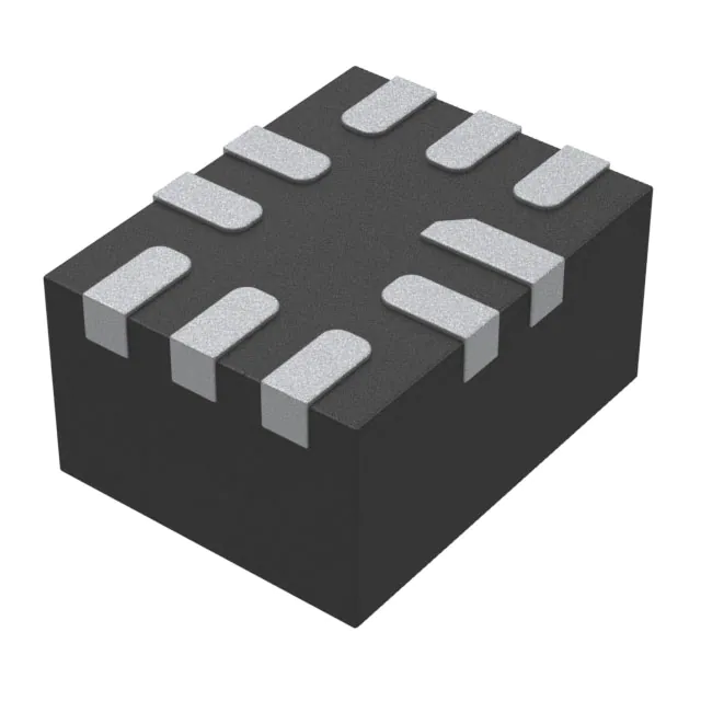
- Part No.:
- MP3309CGQG-P
- Manufacturer:
- Monolithic Power Systems Inc.
- Category:
- LED Drivers
- Package:
- 10-VFQFN
- Datasheet:
-
 MP3309CGQG-P.pdf
- Description:
- IC LED DRVR RGLTR PWM 1.5A 10QFN
- Quantity:
- Payment:

- Shipping:

Inventory:1,289
Please send an inquiry. Send us your inquiry, and we will respond immediately.
Product details
Overview
MP3309CGQG-P from Monolithic Power Systems is a white LED step-up converter IC with I²C interface, designed for backlighting in compact portable displays. It operates from 2.7V–5.5V input, delivers up to 38V output, supports programmable switching frequency (300–1200 kHz), regulates LED current via 200mV ±1% feedback voltage, and integrates synchronous rectification with selectable non-synchronous mode for efficiency optimization in smartphones and tablets.
For engineers reviewing the MP3309CGQG-P datasheet, MP3309CGQG-P pinout, MP3309CGQG-P application, or MP3309CGQG-P equivalent, key selection criteria include its I²C-programmable OVP thresholds (13.5V/24V/35.5V), dual dimming support (analog via register + PWM on EN/PWML), thermal shutdown at 150°C, cycle-by-cycle current limit of 1.5A, and QFN-10 (1.4×1.8mm) package for space-constrained PCB layouts.
Technical Context
The MP3309CGQG-P uses peak-current-mode control with internal ramp compensation to stabilize operation above 50% duty cycle. Its error amplifier compares FB voltage against a digitally adjustable 200mV reference (31-step I²C-controlled range: 0–200mV), enabling precise analog dimming without external DACs.
Switching frequency is resistor-programmed (FREQ pin) from 300kHz to 1.2MHz, directly impacting inductor size and EMI performance. The I²C interface (400kHz, address 0x17) configures protection thresholds (OVP0/OVP1), dimming mode (DIMS), synchronous mode (SYNC), and enables/disables the IC-enabling dynamic system-level fault response and adaptive power management.
Key Specifications
| Parameter | Value and Actual Design Meaning |
|---|---|
| Input Voltage | 2.7V–5.5V: Supports single-cell Li-ion (3.0–4.2V) and USB-powered systems without LDO pre-regulation. |
| Output Voltage | Up to 38V: Drives 8-series white LEDs (≈3.2V each) or 3×3 LED arrays with margin for forward voltage variation. |
| Feedback Voltage | 200mV ±1%: Enables low-loss current sensing with 10Ω resistor for 20mA LED current; reduces heat and PCB area vs. higher-voltage references. |
| Switching Frequency | 300–1200 kHz: Programmable via FREQ pin resistor; higher frequencies allow smaller inductors but increase MOSFET switching loss. |
| I²C Interface | 400kHz, address 0x17: Allows real-time OVP threshold selection (13.5V/24V/35.5V), dimming mode control, and fault register readback (LEDO/OTP/VOS). |
| Thermal Shutdown | 150°C with 25°C hysteresis: Prevents permanent damage during sustained overload; resumes operation only after die cools below 125°C. |
| Cycle-by-Cycle Limit | 1.5A: Protects internal MOSFETs during short-circuit or startup inrush; limits peak inductor current in continuous conduction mode. |
Pinout & Package
MP3309CGQG-P is housed in a thermally enhanced 10-pin QFN package (1.4mm × 1.8mm, 0.4mm pitch) with exposed thermal pad for efficient heat dissipation in high-density mobile PCBs.
| Pin/Terminal | Circuit Role | Design Meaning |
|---|---|---|
| 1 SDA | I²C data line | Bi-directional serial data interface for configuring registers and reading fault status (LEDO/OTP/VOS). |
| 2 VIN | Main power input | Supplies internal logic and gate drivers; requires local 4.7μF ceramic bypass capacitor to suppress high-frequency ripple. |
| 3 EN/PWML | Enable & PWM dimming input | Active-high enable; accepts 100Hz–2kHz PWM signal for brightness control; >20ms low pulse forces shutdown. |
| 4 FREQ | Frequency programming node | Connects to GND via resistor (e.g., 200kΩ → 600kHz); floating state invalid; sets oscillator timing for EMI and efficiency trade-offs. |
| 5 FB | Current sense feedback | Regulates voltage across external sense resistor to 200mV; determines LED current (ILED = 0.2V / RFB). |
| 6 GND | Power and signal ground | Common reference for all analog/digital circuits; must be low-impedance connection to thermal pad for thermal stability. |
| 7 SW | Switch node | Drain of internal low-side N-MOSFET; connects to inductor; carries high di/dt; critical for EMI loop minimization. |
| 8 VOUT | Boost output | Source of internal synchronous MOSFET; supplies LED string; requires 0.47μF X7R ceramic capacitor for ripple suppression. |
| 9 BST | Bootstrap supply | Connects to SW via 0.1μF capacitor to generate gate drive voltage for synchronous MOSFET; enables high-side switching. |
| 10 SCL | I²C clock line | 400kHz master-generated clock; controls timing of register writes/reads; requires pull-up to VIN for proper logic levels. |
Key Features
| Feature | Design Value |
|---|---|
| Synchronous/non-synchronous mode select | Configurable via I²C SYNC bit: synchronous mode eliminates Schottky diode (reducing BOM cost and footprint); non-synchronous mode avoids gate driver loss at high duty cycles or frequencies. |
| Digitally programmable OVP thresholds | Three user-selectable points (13.5V/24V/35.5V) via OVP0/OVP1 bits: allows matching capacitor voltage rating to application needs-e.g., 16V cap for 3×3 LED array with 24V OVP. |
| Soft-start with slew-rate controlled reference | 32-step ramp (320μs/step) from 0 to 200mV: prevents inrush current during startup; combined with 0.7A current limit for first 5ms, ensures safe cold-start into capacitive loads. |
| I²C fault register monitoring | Read-only LEDO (open-string), OTP (over-temperature), and VOS (VOUT-to-GND short) bits: enables host MCU to log faults and trigger graceful degradation instead of uncontrolled shutdown. |
| Low-quiescent current operation | 420μA typical IQ in active mode; 1μA in shutdown: extends battery life in always-on display subsystems without compromising responsiveness. |
Applications
| Smartphone Backlighting | Tablet Display Backlight |
|---|---|
|
Use Scenario: Driving 8-series white LEDs (24–28V nominal) in a bezel-constrained smartphone display module. IC Role / Device Role / Timing Role: WLED boost controller with I²C-configurable OVP and analog dimming for seamless brightness transitions under Android HAL control. Use Value: 200mV feedback reference minimizes sense resistor power loss; QFN-10 package fits tight board space; 35.5V default OVP protects against open-string failure in high-Vf LED strings. |
Use Scenario: Powering a 3×3 LED array (≈12V nominal) in a 10-inch tablet with dynamic local dimming zones. IC Role / Device Role / Timing Role: Digitally addressable LED driver enabling per-zone brightness control via I²C writes to DIMS and D0–D4 registers. Use Value: 400kHz I²C interface allows rapid reconfiguration between dimming modes; programmable 24V OVP permits use of lower-cost 25V output capacitors. |
| Feature Phone Keypad Illumination | Portable Medical Display Backlight |
|
Use Scenario: Low-cost keypad backlight using 3–4 series LEDs (≈10–12V) powered from single AA/AAA battery (1.5V) with boost. IC Role / Device Role / Timing Role: High-efficiency step-up converter with UVLO (2.5V) and PWM dimming for tactile feedback illumination. Use Value: 2.7V minimum input enables operation down to ~1.8V battery voltage with minimal dropout; EN/PWML pin supports simple microcontroller GPIO dimming. |
Use Scenario: Reliable backlight for ruggedized medical tablet used in operating rooms with strict thermal and fault-reporting requirements. IC Role / Device Role / Timing Role: Safety-aware LED driver with readback-capable fault registers (OTP, LEDO, VOS) for diagnostic logging and fail-safe behavior. Use Value: Thermal shutdown at 150°C with 25°C hysteresis prevents thermal runaway; I²C fault bits allow host MCU to initiate alarm or display warning before catastrophic failure. |
Equivalent & Alternatives
The following parts are listed as comparable options for similar white LED boost driver applications.
| Alternative Part | Technical Difference | Application Difference | Selection Advice |
|---|---|---|---|
| RT9397BZSP | Fixed 1.2MHz fSW; no I²C interface; analog dimming only via EN pin; 30V max output; 1.2A current limit. | Lacks digital OVP configuration and fault reporting; suitable only for static backlight designs without dynamic adjustment. | Select when cost sensitivity outweighs configurability; avoid if system requires runtime OVP changes or fault diagnostics. |
| TPS61165DRVR | 2.7–6V input; 28V max output; I²C-compatible but 100kHz max clock; no programmable OVP; 1.2A current limit. | Lower max output voltage restricts LED string length; slower I²C limits update rate for multi-zone dimming. | Prefer for TI-ecosystem designs where 28V output suffices and I²C bandwidth is not critical; verify thermal derating at 125°C ambient. |
Compared with RT9397BZSP and TPS61165DRVR, the MP3309CGQG-P provides superior flexibility through its 300–1200kHz programmable fSW, three-point OVP selection, and full I²C register access-including fault status readback-making it optimal for adaptive, safety-critical, or space-constrained portable display systems.
Availability
MP3309CGQG-P is available at Aetrix Electronics and suitable for smartphone backlighting, tablet display modules, feature phone keypad illumination, and portable medical display backlighting requiring stable component supply across production lifecycles.
Supply support for MP3309CGQG-P includes scheduled delivery planning, volume procurement assistance, BOM continuity management, traceable sourcing, and lifecycle availability coordination for OEM customers, industrial embedded developers, connected-device designers, and electronics production programs.
Manufacturer
Monolithic Power Systems (MPS) is a fabless semiconductor company specializing in high-performance analog and mixed-signal ICs for power management, motion control, and automotive applications.
The MP3309CGQG-P belongs to MPS's WLED boost driver product line, engineered specifically for energy-efficient, digitally configurable backlighting in space- and thermal-constrained portable electronics.
FAQ
What is the maximum LED string voltage supported by MP3309CGQG-P?
The MP3309CGQG-P supports up to 38V output, verified by absolute maximum rating (VOUT ≤ +40V) and typical application validation with 8-series white LEDs (~28V nominal). This enables driving longer LED strings than competitors limited to 28–30V, reducing the need for parallel strings and associated current-matching complexity.
How does the I²C interface configure LED current without an external DAC?
The MP3309CGQG-P uses a 5-bit internal reference register (D0–D4) to set the feedback reference voltage from 0mV to 200mV in 31 discrete steps. Since LED current is calculated as ILED = VREF/RFB, writing to this register digitally adjusts current amplitude-eliminating external DACs while maintaining ±1% accuracy at room temperature.
Can MP3309CGQG-P operate in non-synchronous mode, and why would I choose it?
Yes-setting the SYNC bit to '0' disables the internal synchronous MOSFET, requiring an external Schottky diode between SW and VOUT. This mode is preferred when LED string voltage is high (large duty cycle) or switching frequency exceeds 800kHz, where synchronous gate driver losses dominate efficiency. It trades BOM simplicity for thermal and efficiency optimization in specific operating points.
What protection features are readable via I²C, and how are they used?
The MP3309CGQG-P exposes three read-only fault bits via I²C register 0x01: LEDO (open-string), OTP (over-temperature), and VOS (VOUT-to-GND short). Host MCUs can poll these bits to distinguish fault causes-e.g., triggering different recovery sequences (cool-down delay for OTP vs. LED replacement alert for LEDO)-enabling robust system-level diagnostics without additional sensors.
What is the minimum recommended input capacitance, and why is dielectric type important?
A minimum 2.2μF X5R or X7R ceramic capacitor is recommended at VIN. These dielectrics maintain stable capacitance under DC bias and temperature-critical because input capacitor impedance at the switching frequency must stay below source impedance to prevent noise coupling. Using Y5V or Z5U types risks >50% capacitance loss at rated voltage, degrading ripple suppression and EMI performance.
How does the soft-start sequence prevent inrush current during power-up?
The MP3309CGQG-P implements a 32-step reference voltage ramp (320μs per step, total 10.24ms) from 0 to 200mV, combined with a reduced 0.7A cycle-by-cycle current limit active for the first 5ms. This coordinated approach limits peak inductor current and output capacitor charging surge-preventing voltage droop on shared rails and avoiding false UVLO triggers in multi-rail systems.
Is the thermal pad on the QFN-10 package required to be soldered, and what is its electrical role?
Yes-the exposed thermal pad must be soldered to a dedicated PCB copper pour connected to GND. It serves both thermal and electrical functions: lowering θJA from 140°C/W to ~45°C/W in standard layouts, and providing the primary return path for internal power MOSFET currents. Omitting this connection risks thermal shutdown at <50% load and violates JEDEC MO-220 mechanical compliance.
MP3309CGQG-P Specifications
- Product attributes
- Attribute value
- Manufacturer:
- Monolithic Power Systems Inc.
- Series:
- -
- Package/Case:
- 10-VFQFN
- Packaging:
- Tape & Reel (TR)
- Product Status:
- Active
- Type:
- DC DC Regulator
- Topology:
- Step-Up (Boost)
- Internal Switch(s):
- Yes
- Number of Outputs:
- 1
- Voltage - Supply (Min):
- 2.7V
- Voltage - Supply (Max):
- 5.5V
- Voltage - Output:
- 35V
- Current - Output / Channel:
- 1.5A
- Frequency:
- 640kHz
- Dimming:
- Analog, PWM
- Applications:
- Backlight
- Operating Temperature:
- -40°C ~ 125°C (TJ)
- Grade:
- -
- Qualification:
- -
- Mounting Type:
- Surface Mount
- Supplier Device Package:
- 10-QFN (1.4x1.8)
MP3309CGQG-P FAQ
1.How can I place an order for MP3309CGQG-P through Aetrix?
Please submit a Request for Quotation (RFQ) for MP3309CGQG-P on Aetrix. Our sales agent will provide a competitive quotation and guide you through the order confirmation once you accept the terms.
2.Are the price and stock information for MP3309CGQG-P reliable?
The price and inventory of MP3309CGQG-P are updated periodically and may fluctuate due to market conditions. Stock and pricing data are typically refreshed every 24 hours. Quotation validity for MP3309CGQG-P is usually 5 days.
3.What payment methods are accepted for MP3309CGQG-P?
We accept Wire Transfer, PayPal, Credit Card, Western Union, MoneyGram, and Escrow for MP3309CGQG-P transactions.
Note: Certain payment methods may incur a processing fee.
4.How is shipping managed for MP3309CGQG-P?
MP3309CGQG-P orders can be shipped via leading logistics carriers, including DHL, UPS, FedEx, TNT, or Registered Mail.
Once your MP3309CGQG-P order is processed, you will receive an email with the shipment details and tracking number.
Note: Tracking information may take up to 24 hours to appear. Express delivery typically takes 3–5 business days.
5.How can I obtain technical support or documentation for MP3309CGQG-P?
For technical support, including MP3309CGQG-P datasheets, pinout diagrams, or application guidance, please contact our engineering support team. They can provide detailed documentation and assistance for your MP3309CGQG-P requirements.
6.How does Aetrix verify that MP3309CGQG-P is sourced from the original manufacturer or authorized distributors?
All MP3309CGQG-P products on Aetrix are procured from qualified distributors and authorized channels. Our dedicated quality assurance team conducts strict verification, including traceability checks and, if necessary, third-party testing. This ensures that MP3309CGQG-P meets industry standards.
7.What is the process for return or replacement of MP3309CGQG-P?
All MP3309CGQG-P units undergo pre-shipment inspection (PSI). If there is an issue with MP3309CGQG-P, returns or replacements are accepted under the following conditions:
1.Quantity discrepancies, incorrect items, or visible external defects (such as breakage or corrosion), acknowledged by Aetrix.
2.The issue is reported within 90 days of delivery.
3.The MP3309CGQG-P part is unused and in its original packaging.
Return procedure for MP3309CGQG-P:
1.Submit a request within 90 days.
2.Obtain a Return Material Authorization (RMA) from Aetrix.
MP3309CGQG-P Tags

-
BCR402RE6327HTSA1
Infineon Technologies

-
BCR430UXTSA2
Infineon Technologies

-
BCR420UE6433HTMA1
Infineon Technologies
-
BCR420UE6327HTSA1
Infineon Technologies
-
BCR421UE6327HTSA1
Infineon Technologies

-
LYT1604D-TL
Power Integrations

-
HV9910CLG-G
Microchip Technology

-
CL2N8-G
Microchip Technology

-
BCR420UW6-7
Diodes Incorporated
-
BCR421UW6-7
Diodes Incorporated

-
BCR420UFD-7
Diodes Incorporated
-
BCR421UFD-7
Diodes Incorporated
Tech Hub

Operational amplifier guide covering op amp basics, feedback, ideal vs real op amps, common configurations, buffer circuits, offset, bias current, gain-bandwidth, slew rate, rail-to-rail limits and sel…

Jumper cables guide covering safe connection order, red and black clamp placement, final ground connection, cable gauge, length, clamp quality, copper vs CCA cables, jump starter comparison and battery…

LDO regulator guide covering low dropout voltage, power dissipation, thermal design, PSRR, output noise, capacitor stability, adjustable LDO circuits, LDO vs buck converter and datasheet selection chec…

Conditional Access Module guide covering CAM meaning, CI/CI+ interface, smart card authorization, DVB security workflow, TV and set-top box compatibility, internal electronics, ESD protection, connecto…

Guide to electronic component obsolescence covering EOL risk, PCN/PDN notices, last-time buy planning, replacement options, form-fit-function validation, counterfeit risk and BOM lifecycle management.

18650 battery guide covering lithium-ion cell basics, 3.6V/3.7V voltage, 4.2V charging, mAh and Wh capacity, protected cells, chargers, BMS, series-parallel packs, holders, welding and sourcing checks.…

Hall effect sensor guide covering working principle, linear and digital sensors, Arduino circuits, current sensing, speed detection, automotive applications, A3144 examples, signal filtering and datash…

Product Change Notification guide for electronic components, covering PCN meaning, PCN vs PDN/EOL, common change types, risk levels, form-fit-function review, engineering validation, BOM control, LTB/L…

A practical guide to blend door actuators, covering HVAC function, symptoms, location, AC and heater issues, reset and calibration, replacement cost, electrical diagnosis, compatibility checks, and rep…

Engineering guide to Raspberry Pi alternatives, covering chip-level differences, Orange Pi, ROCK, Jetson, Banana Pi, NanoPi, Compute Module, Pico, GPIO, camera, HAT compatibility, and replacement risks…


