
 My Inquiry
 My Account


Monolithic Power Systems Inc. MP3331GC-P
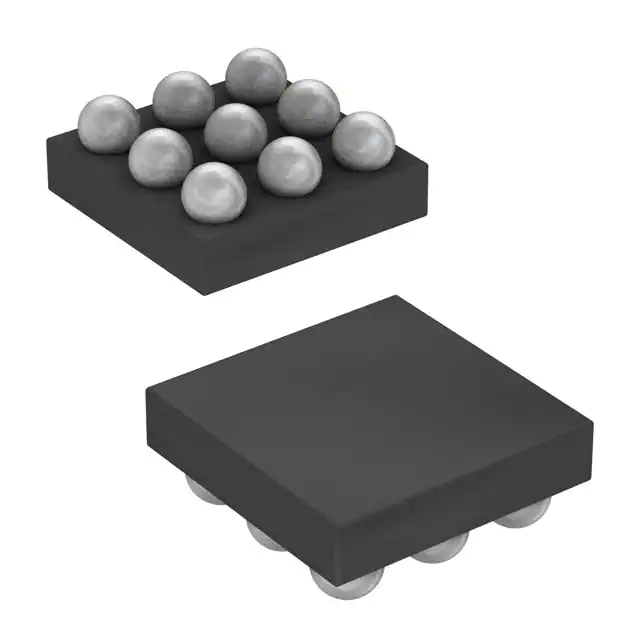
- Part No.:
- MP3331GC-P
- Manufacturer:
- Monolithic Power Systems Inc.
- Category:
- LED Drivers
- Package:
- 9-WFBGA, WLCSP
- Datasheet:
-
 MP3331GC-P.pdf
- Description:
- IC LED DRVR RGLTR PWM 2A 9WLCSP
- Quantity:
- Payment:

- Shipping:

Inventory:3,046
Please send an inquiry. Send us your inquiry, and we will respond immediately.
Product details
Overview
MP3331GC-P from Monolithic Power Systems is a 2A synchronous boost flash LED driver with I²C interface, designed for single-channel high-resolution camera flash applications. It delivers programmable flash current up to 2A (±7% accuracy), operates from 2.7V–5.5V input, supports 1/2/3/4MHz selectable switching frequency, and features GND-referenced LED cathode for improved thermal performance in compact mobile camera modules.
For engineers reviewing the MP3331GC-P datasheet, MP3331GC-P pinout, MP3331GC-P application, or MP3331GC-P equivalent, key selection criteria include I²C-configurable flash/assist/torch/indicator/5V DC modes, integrated over-voltage, over-temperature, LED short/open, and low-battery protection - all in a WLCSP9-1.7mm × 1.7mm package.
Technical Context
The MP3331GC-P integrates a synchronous boost converter with peak-current-mode PWM control, supporting hardware- or software-triggered flash operation via STR/TOR pins and register-controlled mode transitions. Its adaptive switching frequency foldback (4MHz → 1MHz) and pass-mode operation minimize power loss when VIN approaches VOUT.
It implements dual-loop regulation: current-source control for flash/assist/torch/indicator modes and voltage-loop takeover in 5V DC output mode. Protection logic includes time-out detection (200ms default), adaptive thermal threshold (130°C), and real-time fault reporting via I²C status registers (FT_OTP, FT_VBATL, FT_LEDSC, etc.).
Key Specifications
| Parameter | Value and Actual Design Meaning |
|---|---|
| Input Voltage Range | 2.7V–5.5V - Supports direct connection to Li-ion/Li-poly battery rails without pre-regulation. |
| Max Flash Current | 2A ±7% - Programmable via I²C register I_FL; enables high-intensity still-image capture in low-light. |
| Switching Frequency | 1/2/3/4MHz selectable - Optimizes PCB size (smaller inductors/caps) and EMI profile per system layout. |
| I²C Interface Speed | 400kHz - Compatible with standard fast-mode microcontrollers; supports real-time mode and current reconfiguration. |
| LED Cathode Reference | GND-referenced - Enables direct thermal coupling to PCB ground plane, improving thermal resistance by ~30% vs. floating cathode. |
| Protection Functions | LED short/open, VOUT-GND short, over-voltage (5.5V), over-temperature (150°C shutdown), low-battery lockout - Reduces need for external fault monitoring circuitry. |
| Package | WLCSP9-1.7mm × 1.7mm - Ultra-compact footprint for space-constrained mobile camera modules; 0.4mm pitch, bottom-side solder balls. |
Pinout & Package
MP3331GC-P uses a 9-ball Wafer-Level Chip-Scale Package (WLCSP) measuring 1.7mm × 1.7mm with 0.4mm ball pitch. The package exposes no die pad; thermal dissipation occurs through solder balls to PCB copper.
| Pin/Terminal | Circuit Role | Design Meaning |
|---|---|---|
| A1 OUT | Boost converter output | High-current node delivering regulated voltage to LED anode; requires local ceramic decoupling (≥10μF). |
| A2 SW | Switching node | Connection point between internal NMOS/PMOS switches and external inductor; high dv/dt node requiring tight layout. |
| A3 GND | Power and signal ground | Common reference for all analog/digital circuits; must be connected to low-impedance PCB ground plane. |
| B1 LED | LED current sink | Sinks up to 2A from LED anode; cathode tied to GND - simplifies thermal path and reduces parasitic inductance. |
| B2 STR | Strobe synchronization input | Hardware trigger for flash timing; level- or edge-sensitive; internally weakly pulled low when floating. |
| B3 IN | Input supply | Primary power input (2.7–5.5V); bypass capacitor required within 2mm of pin for stability. |
| C1 TOR/TX | Torch or RF transmission sync input | Dual-function pin: torch enable or TX current reduction signal; active-high; internally weakly pulled low. |
| C2 SDA | I²C data line | Open-drain bidirectional data bus; requires external pull-up (typically 2.2kΩ to 3.3V). |
| C3 SCL | I²C clock line | Open-drain clock input; supports 400kHz fast-mode; same pull-up as SDA. |
Key Features
| Feature | Design Value |
|---|---|
| Programmable flash current | 0–2A in 32 steps (±7% accuracy) - Enables precise luminance control across varying battery SOC and ambient temperature. |
| Multi-mode operation | Flash/assist/torch/indicator/5V DC - Single IC replaces discrete solutions for camera UI lighting and auxiliary power. |
| Pre-flash low-battery detection | Measures actual flash current drop during pre-flash and reports IFL_MIN - Allows host MCU to adjust main-flash intensity preemptively. |
| Adaptive thermal management | Reduces flash current to I_TX at 130°C junction; shuts down at 150°C - Prevents thermal runaway without external sensors. |
| Integrated fault reporting | Eight-bit status register (0xBH/0xCH) with dedicated bits for VBATL, OVP, LEDSC, OTP, TO, TX - Enables rapid diagnostics without oscilloscope probing. |
Applications
| Smartphone Camera Flash | Tablet Front-Facing Illumination |
|---|---|
|
Use Scenario: High-intensity flash for still-image capture in sub-10lux environments on flagship smartphones. IC Role / Device Role / Timing Role: Primary flash current source synchronized to image sensor exposure via STR pin; operates in hardware level-sensitive flash mode with 100ms FL_TIM. Use Value: Delivers 2A stable current with <5µs TX-induced current settling - ensures consistent exposure across multiple frames during burst capture. |
Use Scenario: Low-power assist light for video conferencing in tablets under dim indoor lighting. IC Role / Device Role / Timing Role: Torch-mode current source (≤508mA) controlled via I²C register I_TOR; enabled by TOR/TX high pulse. Use Value: Achieves flicker-free illumination using 31.5kHz PWM dimming in indicator mode - eliminates visible strobing during video calls. |
| Digital Still Camera Auxiliary Light | Mobile Device 5V Power Rail Generation |
|
Use Scenario: Compact DSC requiring auto-focus assist beam and red-eye reduction flash in one optical path. IC Role / Device Role / Timing Role: Dual-role driver: assist mode (508mA) for AF beam, flash mode (2A) for main exposure - switched via LED_MOD register. Use Value: Eliminates need for separate assist LED driver; shared current-sense path ensures matched color temperature between assist and flash LEDs. |
Use Scenario: On-demand 5V rail for USB peripherals or sensors in portable devices with limited board space. IC Role / Device Role / Timing Role: Fixed 5V DC output regulator activated by 5V_MOD=1; maintains regulation even while LED_EN=0 to avoid cross-conduction. Use Value: Provides 5V/500mA capability without external LDO; thermal derating managed via junction temperature monitoring and fault register readback. |
Equivalent & Alternatives
The following parts are listed as comparable options for similar flash LED driver applications.
| Alternative Part | Technical Difference | Application Difference | Selection Advice |
|---|---|---|---|
| MP3331-C09W | Pin-compatible revision with updated thermal shutdown threshold (145°C vs. 150°C) and enhanced low-battery hysteresis. | Recommended for new designs; supports same modes and register map but adds factory-programmed top marking for traceability. | Select MP3331-C09W for production builds requiring long-term availability and documented lifecycle support. |
| RT8542GQW | 2.5A flash driver with analog current control (no I²C), fixed 2MHz switching, no 5V DC mode or pre-flash reporting. | Limited to basic flash/torch functions; lacks multi-mode flexibility and diagnostic registers - suitable only for cost-sensitive legacy designs. | Choose only if I²C configurability, thermal adaptability, and fault visibility are not required. |
Compared with MP3331GC-P, MP3331-C09W offers extended thermal margin and formal obsolescence planning, while RT8542GQW trades intelligence for lower BOM count - making MP3331GC-P optimal where firmware-controlled lighting behavior and field diagnostics are essential.
Availability
MP3331GC-P is available at Aetrix Electronics and suitable for smartphone camera modules, tablet imaging subsystems, and digital still camera auxiliary lighting requiring stable component supply and full technical documentation support.
Supply support for MP3331GC-P includes scheduled delivery planning, volume procurement assistance, BOM continuity management, traceable sourcing, and lifecycle availability coordination for OEM customers, industrial embedded developers, connected-device designers, and electronics production programs.
Manufacturer
Monolithic Power Systems (MPS) is a fabless semiconductor company specializing in high-performance power management ICs, with design centers in the US, China, and Taiwan, and global manufacturing partnerships.
The MP3331 product line targets mobile imaging systems requiring high-efficiency, small-footprint flash drivers with intelligent protection and multi-mode flexibility - directly addressing thermal, size, and firmware integration constraints in modern camera modules.
FAQ
What does "NOT RECOMMENDED FOR NEW DESIGNS" mean for MP3331GC-P?
This designation indicates MPS has released an improved revision (MP3331-C09W) with enhanced thermal specifications and formal lifecycle support. MP3331GC-P remains fully functional and available for existing designs, but new projects should adopt MP3331-C09W for long-term supply assurance and updated reliability data.
How does the pre-flash low-battery detection work?
During pre-flash, the MP3331GC-P monitors actual delivered current (IFL_ACT) and records the minimum sustained value (IFL_MIN) in register 0x09. Host firmware reads IFL_MIN to scale main-flash current, preventing underexposure caused by battery voltage sag - no external ADC or polling required.
Can MP3331GC-P drive multiple LEDs in series?
No. The MP3331GC-P is a single-channel current sink with GND-referenced LED terminal. It supports only one LED (or parallel-connected LEDs sharing identical Vf) per device. Driving series LEDs would require floating-cathode topology, which this IC does not implement.
What is the purpose of the TOR/TX pin in flash mode?
In flash mode, TOR/TX acts exclusively as a TX (transmit) pin. When driven high, it forces immediate reduction of flash current to the I_TX register value (<5µs settling), enabling RF transmission synchronization without interrupting exposure timing - critical for cellular/WiFi coexistence.
Is the WLCSP9 package compatible with standard reflow profiles?
Yes. The MP3331GC-P WLCSP9 package is qualified for IPC/JEDEC J-STD-020D reflow, with peak temperature ≤260°C and time above liquidus (TAL) of 60–150 seconds. Thermal resistance θJA = 110°C/W on a 4-layer JEDEC test board confirms compatibility with standard mobile PCB stackups.
Does MP3331GC-P support automatic mode transition from torch to flash?
Yes. When operating in torch mode (TOR/TX = high, LED_MOD = 00), a rising edge on STR automatically triggers flash mode with current ramp-up governed by I_FL and TUP_I registers - eliminating host MCU intervention for seamless transition during video recording with flash assist.
How is LED open-circuit detected?
LED open is detected when VOUT − VLED < 90mV AND VOUT > 5.5V - indicating no current flow through the LED while output voltage exceeds over-voltage threshold. The IC stops switching, resets mode bits, and sets FT_LEDOP and FT_OVP flags in register 0x0B/0x0C.
MP3331GC-P Specifications
- Product attributes
- Attribute value
- Manufacturer:
- Monolithic Power Systems Inc.
- Series:
- -
- Package/Case:
- 9-WFBGA, WLCSP
- Packaging:
- Tape & Reel (TR)
- Product Status:
- Not For New Designs
- Type:
- DC DC Regulator
- Topology:
- Step-Up (Boost)
- Internal Switch(s):
- Yes
- Number of Outputs:
- 1
- Voltage - Supply (Min):
- 2.7V
- Voltage - Supply (Max):
- 5.5V
- Voltage - Output:
- -
- Current - Output / Channel:
- 2A
- Frequency:
- 4MHz
- Dimming:
- PWM
- Applications:
- Camera Flash
- Operating Temperature:
- -40°C ~ 125°C (TJ)
- Grade:
- -
- Qualification:
- -
- Mounting Type:
- Surface Mount
- Supplier Device Package:
- 9-WLCSP (1.7x1.7)
MP3331GC-P FAQ
1.How can I place an order for MP3331GC-P through Aetrix?
Please submit a Request for Quotation (RFQ) for MP3331GC-P on Aetrix. Our sales agent will provide a competitive quotation and guide you through the order confirmation once you accept the terms.
2.Are the price and stock information for MP3331GC-P reliable?
The price and inventory of MP3331GC-P are updated periodically and may fluctuate due to market conditions. Stock and pricing data are typically refreshed every 24 hours. Quotation validity for MP3331GC-P is usually 5 days.
3.What payment methods are accepted for MP3331GC-P?
We accept Wire Transfer, PayPal, Credit Card, Western Union, MoneyGram, and Escrow for MP3331GC-P transactions.
Note: Certain payment methods may incur a processing fee.
4.How is shipping managed for MP3331GC-P?
MP3331GC-P orders can be shipped via leading logistics carriers, including DHL, UPS, FedEx, TNT, or Registered Mail.
Once your MP3331GC-P order is processed, you will receive an email with the shipment details and tracking number.
Note: Tracking information may take up to 24 hours to appear. Express delivery typically takes 3–5 business days.
5.How can I obtain technical support or documentation for MP3331GC-P?
For technical support, including MP3331GC-P datasheets, pinout diagrams, or application guidance, please contact our engineering support team. They can provide detailed documentation and assistance for your MP3331GC-P requirements.
6.How does Aetrix verify that MP3331GC-P is sourced from the original manufacturer or authorized distributors?
All MP3331GC-P products on Aetrix are procured from qualified distributors and authorized channels. Our dedicated quality assurance team conducts strict verification, including traceability checks and, if necessary, third-party testing. This ensures that MP3331GC-P meets industry standards.
7.What is the process for return or replacement of MP3331GC-P?
All MP3331GC-P units undergo pre-shipment inspection (PSI). If there is an issue with MP3331GC-P, returns or replacements are accepted under the following conditions:
1.Quantity discrepancies, incorrect items, or visible external defects (such as breakage or corrosion), acknowledged by Aetrix.
2.The issue is reported within 90 days of delivery.
3.The MP3331GC-P part is unused and in its original packaging.
Return procedure for MP3331GC-P:
1.Submit a request within 90 days.
2.Obtain a Return Material Authorization (RMA) from Aetrix.
MP3331GC-P Tags

-
BCR402RE6327HTSA1
Infineon Technologies

-
BCR430UXTSA2
Infineon Technologies

-
BCR420UE6433HTMA1
Infineon Technologies
-
BCR420UE6327HTSA1
Infineon Technologies
-
BCR421UE6327HTSA1
Infineon Technologies

-
LYT1604D-TL
Power Integrations

-
HV9910CLG-G
Microchip Technology

-
CL2N8-G
Microchip Technology

-
BCR420UW6-7
Diodes Incorporated
-
BCR421UW6-7
Diodes Incorporated

-
BCR420UFD-7
Diodes Incorporated
-
BCR421UFD-7
Diodes Incorporated
Tech Hub

Operational amplifier guide covering op amp basics, feedback, ideal vs real op amps, common configurations, buffer circuits, offset, bias current, gain-bandwidth, slew rate, rail-to-rail limits and sel…

Jumper cables guide covering safe connection order, red and black clamp placement, final ground connection, cable gauge, length, clamp quality, copper vs CCA cables, jump starter comparison and battery…

LDO regulator guide covering low dropout voltage, power dissipation, thermal design, PSRR, output noise, capacitor stability, adjustable LDO circuits, LDO vs buck converter and datasheet selection chec…

Conditional Access Module guide covering CAM meaning, CI/CI+ interface, smart card authorization, DVB security workflow, TV and set-top box compatibility, internal electronics, ESD protection, connecto…

Guide to electronic component obsolescence covering EOL risk, PCN/PDN notices, last-time buy planning, replacement options, form-fit-function validation, counterfeit risk and BOM lifecycle management.

18650 battery guide covering lithium-ion cell basics, 3.6V/3.7V voltage, 4.2V charging, mAh and Wh capacity, protected cells, chargers, BMS, series-parallel packs, holders, welding and sourcing checks.…

Hall effect sensor guide covering working principle, linear and digital sensors, Arduino circuits, current sensing, speed detection, automotive applications, A3144 examples, signal filtering and datash…

Product Change Notification guide for electronic components, covering PCN meaning, PCN vs PDN/EOL, common change types, risk levels, form-fit-function review, engineering validation, BOM control, LTB/L…

A practical guide to blend door actuators, covering HVAC function, symptoms, location, AC and heater issues, reset and calibration, replacement cost, electrical diagnosis, compatibility checks, and rep…

Engineering guide to Raspberry Pi alternatives, covering chip-level differences, Orange Pi, ROCK, Jetson, Banana Pi, NanoPi, Compute Module, Pico, GPIO, camera, HAT compatibility, and replacement risks…


