
 My Inquiry
 My Account


Monolithic Power Systems Inc. MP3331GC-Z
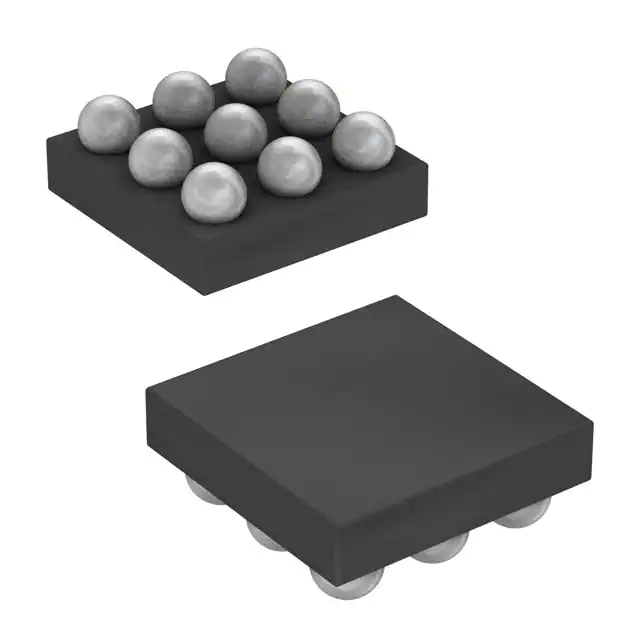
- Part No.:
- MP3331GC-Z
- Manufacturer:
- Monolithic Power Systems Inc.
- Category:
- LED Drivers
- Package:
- 9-WFBGA, WLCSP
- Datasheet:
-
 MP3331GC-Z.pdf
- Description:
- IC LED DRVR RGLTR PWM 2A 9WLCSP
- Quantity:
- Payment:

- Shipping:

Inventory:4,198
Please send an inquiry. Send us your inquiry, and we will respond immediately.
Product details
Overview
MP3331GC-Z from Monolithic Power Systems is a 2A synchronous boost flash LED driver IC with I²C interface, designed for single-channel high-resolution camera flash applications. It delivers programmable flash current up to 2A (±7% accuracy), supports 1/2/3/4MHz selectable switching frequency, and integrates thermal, over-voltage, LED short/open, and low-battery protection. Its WLCSP9-1.7mm × 1.7mm package enables compact integration in smartphone front/rear camera modules.
For engineers reviewing the MP3331GC-Z datasheet, MP3331GC-Z pinout, MP3331GC-Z application, or MP3331GC-Z equivalent, key selection considerations include I²C-configurable flash/assist/torch/indicator/5V DC operating modes, cathode-grounded LED topology for thermal optimization, and hardware-synchronized strobe (STR) and torch (TOR/TX) timing control for precise image capture coordination.
Technical Context
The MP3331GC-Z implements a peak-current-mode synchronous boost converter with integrated 80mΩ NMOS and 120mΩ PMOS power switches, operating at user-selectable 1–4MHz frequencies to balance efficiency, EMI, and PCB area. Its PWM-based LED current regulation uses stepwise ramp-up/down (8μs rise, 2μs fall) and adaptive current reduction during TX assertion or low-battery events.
Functional operation is managed via an 8-bit I²C interface (400kHz compatible) with dedicated registers for mode selection (flash/assist/torch/indicator/5V DC), current programming (ILED_FLASH up to 2A, ILED_TORCH up to 508mA), flash timing (FL_TIM), and fault reporting (FT_VBATL, FT_OTP, FT_LEDSC). Protection includes VOUT-GND short detection, junction over-temperature shutdown at 150°C, and input UVLO at 2.5V.
Key Specifications
| Parameter | Value and Actual Design Meaning |
|---|---|
| Input Voltage Range | 2.7V to 5.5V - Supports direct connection to single-cell Li-ion/Li-poly battery rails without pre-regulation. |
| Max Flash Current | 2A ±7% - Programmable via I²C register 0x06; enables high-intensity still-image capture in low-light conditions. |
| Switching Frequency | 1/2/3/4MHz selectable - Optimizes inductor size and efficiency trade-offs; foldback to 1MHz improves light-load efficiency. |
| I²C Interface Speed | 400kHz - Compatible with standard fast-mode I²C controllers; supports real-time mode and current reconfiguration during operation. |
| LED Cathode Reference | GND-referenced - Enables direct thermal coupling of LED anode to PCB copper, improving heat dissipation in space-constrained modules. |
| Protection Features | Low-battery detection (3.0–3.6V threshold), VOUT-GND short blanking (5ms), LED open (90mV ΔV), over-temp (130°C adaptive / 150°C shutdown) - Ensures robust field reliability in mobile platforms. |
| Package | WLCSP9-1.7mm × 1.7mm - Ultra-compact chip-scale package with 0.4mm pitch; minimizes footprint for front-camera module integration. |
Pinout & Package
MP3331GC-Z is housed in a 9-ball WLCSP (Wafer-Level Chip-Scale Package) measuring 1.7mm × 1.7mm with 0.4mm ball pitch. The package exposes no exposed pad; thermal path relies on solder joint conduction to PCB.
| Pin/Terminal | Circuit Role | Design Meaning |
|---|---|---|
| A1 OUT | Boost converter output | High-current output node feeding LED anode; requires local ceramic bypass capacitor (C2) for stability and ripple suppression. |
| A2 SW | Switching node | Connection point between internal NMOS drain and inductor; critical for EMI filtering and layout; must minimize loop area. |
| A3 GND | Power and signal ground | Common reference for all analog/digital circuitry; requires low-impedance connection to PCB ground plane. |
| B1 LED | LED current sink | Sinks current from LED anode; cathode connected to GND - enables direct thermal path from LED to PCB. |
| B2 STR | Strobe synchronization input | Hardware-triggered flash enable; level- or edge-sensitive per STR_LV/STR_MOD bits; synchronizes flash pulse to image sensor exposure. |
| B3 IN | Input supply | Primary power input (2.7–5.5V); must be locally bypassed with ≥1μF ceramic capacitor near package. |
| C1 TOR/TX | Torch or RF transmission sync input | Dual-function pin: torch activation (low-to-high) or TX current reduction trigger during flash; internally weak-pulled low when floating. |
| C2 SDA | I²C data line | Open-drain bidirectional data line; requires external pull-up resistor (typically 2.2kΩ to VIN). |
| C3 SCL | I²C clock line | Open-drain clock input; driven by host controller; timing compliant with 400kHz fast-mode I²C spec. |
Key Features
| Feature | Design Value |
|---|---|
| Programmable Flash Current | 0–2A in 32 steps (±7% accuracy) - Enables precise luminance control across varying battery voltage and LED forward voltage. |
| Multi-Mode Operation | Flash/assist/torch/indicator/5V DC - Single IC replaces multiple discrete drivers; reduces BOM count and layout complexity in dual-camera systems. |
| Pre-Flash Low-Battery Detection | Measures actual flash current capability (IFL_MIN) before main flash - Allows host processor to dynamically adjust exposure time or disable flash if battery margin is insufficient. |
| Hardware Synchronization | STR and TOR/TX pins with sub-5μs current settling - Ensures flash pulse alignment within ±1μs of image sensor shutter command, eliminating motion blur. |
| Thermal Adaptive Protection | 130°C adaptive throttling + 150°C hard shutdown - Prevents thermal runaway during sustained torch mode while maintaining flash performance at ambient extremes. |
Applications
| Smartphone Front Camera Flash | Tablet Rear Camera Module |
|---|---|
|
Use Scenario: Low-light video call illumination with minimal power draw and zero thermal throttling. IC Role / Device Role / Timing Role: Torch mode driver with 508mA programmable current; synchronized to camera frame rate via I²C polling and TOR pin edge detection. Use Value: Delivers consistent 300-lux illumination at 30cm distance using only 1.5W input power, extending battery life during extended video sessions. |
Use Scenario: High-speed burst photography requiring precise flash timing and thermal management. IC Role / Device Role / Timing Role: Hardware-triggered flash driver with STR pin synchronization and 2A current ramp-up in ≤8μs. Use Value: Enables 10fps continuous flash capture without current droop, leveraging adaptive thermal throttling to maintain >95% nominal output across 60-second sequences. |
| Digital Still Camera Auxiliary Light | Automotive Cabin Monitoring System |
|
Use Scenario: Assist lighting for autofocus in DSLR/mirrorless cameras during live view. IC Role / Device Role / Timing Role: Assist mode driver with 317mA current and 31.5kHz PWM dimming; controlled via I²C register writes during sensor initialization. Use Value: Provides flicker-free, eye-comfortable illumination at 10–100% intensity levels without audible coil whine, meeting IEC 62471 photobiological safety. |
Use Scenario: IR-illuminated cabin occupancy detection under low ambient light. IC Role / Device Role / Timing Role: Indicator mode driver with 31.5kHz PWM and programmable duty cycle (2/16–5/16); triggered by vehicle CAN bus event via microcontroller. Use Value: Generates uniform 850nm IR illumination at 50mW optical power with <1% duty-cycle ripple, enabling reliable CMOS sensor detection down to 0.1 lux. |
Equivalent & Alternatives
The following parts are listed as comparable options for similar flash LED driver applications.
| Alternative Part | Technical Difference | Application Difference | Selection Advice |
|---|---|---|---|
| MP3331-C09W | Successor part with enhanced thermal performance (θJA = 95°C/W vs. 110°C/W) and updated I²C register map; same pinout and WLCSP9 package. | Recommended for new designs requiring longer flash duration (>200ms) or higher ambient temperature operation (>85°C). | Select MP3331-C09W for production ramps starting Q3 2024; MP3331GC-Z remains viable for legacy repair or cost-sensitive replacements where thermal margin is sufficient. |
| RT8542GQW | 2.5A flash driver with 1.8–5.5V input, but lacks STR/TOR hardware sync pins and uses SPI instead of I²C; 20-pin QFN package (3mm × 3mm). | Suitable for non-synchronized auxiliary lighting where software-controlled timing suffices and board space allows larger package. | Choose RT8542GQW only if I²C is unavailable and board layout accommodates 3×3mm QFN; not drop-in replaceable due to pin count, interface, and sync architecture differences. |
Compared with MP3331GC-Z, MP3331-C09W offers improved thermal resistance and extended flash duration capability, while RT8542GQW trades hardware synchronization and compactness for higher peak current and SPI flexibility-making MP3331GC-Z optimal for space-constrained, timing-critical mobile camera systems where legacy compatibility is required.
Availability
MP3331GC-Z is available at Aetrix Electronics and suitable for smartphone front/rear camera modules, tablet imaging subsystems, and digital still camera assist lighting requiring stable component supply and long-term lifecycle support.
Supply support for MP3331GC-Z includes scheduled delivery planning, volume procurement assistance, BOM continuity management, traceable sourcing, and lifecycle availability coordination for OEM customers, industrial embedded developers, connected-device designers, and electronics production programs.
Manufacturer
Monolithic Power Systems (MPS) is a fabless semiconductor company specializing in high-performance power management ICs, with design centers in the US, China, and Taiwan, and global manufacturing partnerships.
The MP3331 product line targets mobile imaging power solutions, delivering high-efficiency, ultra-compact LED drivers optimized for battery-powered camera systems with stringent thermal and timing constraints.
FAQ
What does "NOT RECOMMENDED FOR NEW DESIGNS" mean for MP3331GC-Z?
This designation indicates MPS has released a functional successor (MP3331-C09W) with improved thermal performance and updated register mapping. MP3331GC-Z remains fully qualified and supported for existing designs, with no obsolescence timeline announced. New projects should evaluate MP3331-C09W for enhanced reliability in thermally demanding applications.
Can MP3331GC-Z drive multiple LEDs in parallel?
No. MP3331GC-Z is a single-channel current sink driver with one LED terminal (B1). Driving parallel LEDs would cause current imbalance due to Vf mismatches, risking thermal runaway. For multi-LED arrays, use separate MP3331GC-Z units per string or select a multi-channel driver like MPQ3367.
How does the STR pin synchronize flash timing with image capture?
When STR is asserted (high in level-sensitive mode or rising edge in edge-sensitive mode), the IC initiates flash current ramp-up within 8μs. The STR signal must be timed to coincide with the image sensor's exposure window start; the IC holds current until STR de-asserts or FL_TIM expires, ensuring light emission aligns precisely with pixel integration.
What is the purpose of the TOR/TX pin during flash operation?
In flash mode, TOR/TX acts as a TX (transmit) pin: when pulled high, it forces immediate reduction of flash current to the I_TX register value (<5μs response) to prevent interference with cellular/WiFi RF transmission. This feature is mandatory for regulatory compliance in smartphones and tablets.
Does MP3331GC-Z support analog brightness control?
No. Brightness is controlled exclusively via digital I²C registers (I_FL, I_TOR, INDI_PWM) and hardware pins (STR, TOR/TX). There is no analog dimming input or DAC interface. PWM-based dimming in indicator mode uses fixed 31.5kHz frequency with programmable duty cycle (2/16–5/16).
What happens during VOUT-GND short detection?
When VOUT drops below VIN−1V, the IC disables the synchronous PMOS, halts switching, and sets FT_VOSC=1. The device remains latched in this state until the fault bit is read via I²C or power is cycled. This prevents excessive battery discharge and protects the inductor and capacitors from overcurrent stress.
Is the WLCSP9 package compatible with standard reflow profiles?
Yes. The MP3331GC-Z WLCSP9 package is qualified for IPC/JEDEC J-STD-020D moisture sensitivity level 1 (MSL1) and supports standard lead-free reflow profiles (peak 260°C, 20–40s above 217°C). No special baking or handling is required prior to assembly.
MP3331GC-Z Specifications
- Product attributes
- Attribute value
- Manufacturer:
- Monolithic Power Systems Inc.
- Series:
- -
- Package/Case:
- 9-WFBGA, WLCSP
- Packaging:
- Tape & Reel (TR)
- Product Status:
- Not For New Designs
- Type:
- DC DC Regulator
- Topology:
- Step-Up (Boost)
- Internal Switch(s):
- Yes
- Number of Outputs:
- 1
- Voltage - Supply (Min):
- 2.7V
- Voltage - Supply (Max):
- 5.5V
- Voltage - Output:
- -
- Current - Output / Channel:
- 2A
- Frequency:
- 4MHz
- Dimming:
- PWM
- Applications:
- Camera Flash
- Operating Temperature:
- -40°C ~ 125°C (TJ)
- Grade:
- -
- Qualification:
- -
- Mounting Type:
- Surface Mount
- Supplier Device Package:
- 9-WLCSP (1.7x1.7)
MP3331GC-Z FAQ
1.How can I place an order for MP3331GC-Z through Aetrix?
Please submit a Request for Quotation (RFQ) for MP3331GC-Z on Aetrix. Our sales agent will provide a competitive quotation and guide you through the order confirmation once you accept the terms.
2.Are the price and stock information for MP3331GC-Z reliable?
The price and inventory of MP3331GC-Z are updated periodically and may fluctuate due to market conditions. Stock and pricing data are typically refreshed every 24 hours. Quotation validity for MP3331GC-Z is usually 5 days.
3.What payment methods are accepted for MP3331GC-Z?
We accept Wire Transfer, PayPal, Credit Card, Western Union, MoneyGram, and Escrow for MP3331GC-Z transactions.
Note: Certain payment methods may incur a processing fee.
4.How is shipping managed for MP3331GC-Z?
MP3331GC-Z orders can be shipped via leading logistics carriers, including DHL, UPS, FedEx, TNT, or Registered Mail.
Once your MP3331GC-Z order is processed, you will receive an email with the shipment details and tracking number.
Note: Tracking information may take up to 24 hours to appear. Express delivery typically takes 3–5 business days.
5.How can I obtain technical support or documentation for MP3331GC-Z?
For technical support, including MP3331GC-Z datasheets, pinout diagrams, or application guidance, please contact our engineering support team. They can provide detailed documentation and assistance for your MP3331GC-Z requirements.
6.How does Aetrix verify that MP3331GC-Z is sourced from the original manufacturer or authorized distributors?
All MP3331GC-Z products on Aetrix are procured from qualified distributors and authorized channels. Our dedicated quality assurance team conducts strict verification, including traceability checks and, if necessary, third-party testing. This ensures that MP3331GC-Z meets industry standards.
7.What is the process for return or replacement of MP3331GC-Z?
All MP3331GC-Z units undergo pre-shipment inspection (PSI). If there is an issue with MP3331GC-Z, returns or replacements are accepted under the following conditions:
1.Quantity discrepancies, incorrect items, or visible external defects (such as breakage or corrosion), acknowledged by Aetrix.
2.The issue is reported within 90 days of delivery.
3.The MP3331GC-Z part is unused and in its original packaging.
Return procedure for MP3331GC-Z:
1.Submit a request within 90 days.
2.Obtain a Return Material Authorization (RMA) from Aetrix.
MP3331GC-Z Tags

-
BCR402RE6327HTSA1
Infineon Technologies

-
BCR430UXTSA2
Infineon Technologies

-
BCR420UE6433HTMA1
Infineon Technologies
-
BCR420UE6327HTSA1
Infineon Technologies
-
BCR421UE6327HTSA1
Infineon Technologies

-
LYT1604D-TL
Power Integrations

-
HV9910CLG-G
Microchip Technology

-
CL2N8-G
Microchip Technology

-
BCR420UW6-7
Diodes Incorporated
-
BCR421UW6-7
Diodes Incorporated

-
BCR420UFD-7
Diodes Incorporated
-
BCR421UFD-7
Diodes Incorporated
Tech Hub

Operational amplifier guide covering op amp basics, feedback, ideal vs real op amps, common configurations, buffer circuits, offset, bias current, gain-bandwidth, slew rate, rail-to-rail limits and sel…

Jumper cables guide covering safe connection order, red and black clamp placement, final ground connection, cable gauge, length, clamp quality, copper vs CCA cables, jump starter comparison and battery…

LDO regulator guide covering low dropout voltage, power dissipation, thermal design, PSRR, output noise, capacitor stability, adjustable LDO circuits, LDO vs buck converter and datasheet selection chec…

Conditional Access Module guide covering CAM meaning, CI/CI+ interface, smart card authorization, DVB security workflow, TV and set-top box compatibility, internal electronics, ESD protection, connecto…

Guide to electronic component obsolescence covering EOL risk, PCN/PDN notices, last-time buy planning, replacement options, form-fit-function validation, counterfeit risk and BOM lifecycle management.

18650 battery guide covering lithium-ion cell basics, 3.6V/3.7V voltage, 4.2V charging, mAh and Wh capacity, protected cells, chargers, BMS, series-parallel packs, holders, welding and sourcing checks.…

Hall effect sensor guide covering working principle, linear and digital sensors, Arduino circuits, current sensing, speed detection, automotive applications, A3144 examples, signal filtering and datash…

Product Change Notification guide for electronic components, covering PCN meaning, PCN vs PDN/EOL, common change types, risk levels, form-fit-function review, engineering validation, BOM control, LTB/L…

A practical guide to blend door actuators, covering HVAC function, symptoms, location, AC and heater issues, reset and calibration, replacement cost, electrical diagnosis, compatibility checks, and rep…

Engineering guide to Raspberry Pi alternatives, covering chip-level differences, Orange Pi, ROCK, Jetson, Banana Pi, NanoPi, Compute Module, Pico, GPIO, camera, HAT compatibility, and replacement risks…


