
 My Inquiry
 My Account


Monolithic Power Systems Inc. MP5016HGQH-P
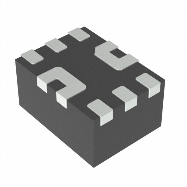
- Part No.:
- MP5016HGQH-P
- Manufacturer:
- Monolithic Power Systems Inc.
- Package:
- 10-PowerVFQFN
- Datasheet:
-
 MP5016HGQH-P.pdf
- Description:
- IC PWR SWITCH N-CHAN 1:1 10QFN
- Quantity:
- Payment:

- Shipping:

Inventory:3,312
Please send an inquiry. Send us your inquiry, and we will respond immediately.
Product details
Overview
MP5016HGQH-P from Monolithic Power Systems is a programmable current-limit switch with integrated 43mΩ N-channel power MOSFET, over-voltage clamp (adjustable 3.9V–21.8V), reverse-current blocking gate driver, and soft-start control via DV/DT pin. It operates from 2.7V to 22V input, delivers up to 5A load current, and protects downstream circuits during hot-swap events in USB PD and SSD power rails.
For engineers reviewing the MP5016HGQH-P datasheet, MP5016HGQH-P pinout, MP5016HGQH-P application, or MP5016HGQH-P equivalent, key selection criteria include adjustable OVP threshold selection via MODE pin, ILIMIT resistor-programmable current limit (0.7–5A), fast 1µs short-circuit response, thermal shutdown at 175°C with 50°C hysteresis, and QFN-10 (1.5mm×2mm) package compatibility with high-density PCB layouts.
Technical Context
The MP5016HGQH-P integrates a precision current-sense amplifier, fast OVP comparator with sub-1µs response, and charge-pump-based gate driver for external reverse-blocking MOSFET control. Its internal logic enables hiccup-mode OCP (2ms on / 700ms off) after sustained overcurrent and foldback current limiting above 11V VDS and 110°C junction temperature.
Soft-start slew rate is programmable via external capacitor on DV/DT pin and MODE pin state (0.4–4.8 V/ms), while OVP clamp voltage is set by MODE digital level (5.75V or 15.2V), floating MODE (no clamp), or resistor-divider (3.9V–21.8V). UVLO threshold is 2.53V with 200mV hysteresis.
Key Specifications
| Parameter | Value and Actual Design Meaning |
|---|---|
| Input Voltage Range | 2.7V to 22V continuous; supports 26V transient - enables use in 12V/19V industrial and USB PD systems without external clamping. |
| Current Limit Range | 0.7A to 5A via ILIMIT resistor; fixed 2.5A when floating - allows precise matching to load requirements while simplifying BOM for standard cases. |
| OVP Clamp Voltage | Programmable 3.9V–21.8V via MODE resistor; 5.75V/15.2V digital select - protects 3.3V/5V/12V loads from overvoltage without external components. |
| RDS(on) | 43mΩ typical at IOUT = 1A - limits conduction loss to <100mW at 2A, reducing thermal stress in compact QFN-10 layout. |
| Short-Circuit Response | 1µs detection and turn-off - prevents >8A peak fault current, minimizing input rail collapse during hard shorts. |
| Thermal Shutdown | 175°C trip with 50°C hysteresis - ensures safe auto-retry operation under sustained overload without latch-off. |
| Quiescent Current | 50µA typical (EN high, MODE float) - enables low-power always-on protection in battery-backed or standby systems. |
Pinout & Package
MP5016HGQH-P is housed in a thermally enhanced QFN-10 package (1.5mm × 2mm, 0.5mm pitch) with exposed thermal pad. The package supports high-current routing and efficient heat dissipation in space-constrained applications such as M.2 SSD modules and USB-C power delivery boards.
| Pin/Terminal | Circuit Role | Design Meaning |
|---|---|---|
| 1, 2 VCC | Supply input | Accepts 2.7–22V input; requires local ceramic decoupling; wide trace recommended for high dI/dt paths. |
| 3 GND | System ground reference | Common return for all internal blocks; must connect directly to thermal pad and low-impedance ground plane. |
| 4 ILIMIT | Current limit programming | Resistor-to-GND sets 0.7–5A limit; floating defaults to 2.5A - eliminates need for trim pot or DAC in most designs. |
| 5 MODE | OVP threshold select | Digital (GND/VCC) or resistor-divider input to configure clamp voltage from 3.9V to 21.8V - enables single-part support across multiple rail voltages. |
| 6, 7 SOURCE | Power MOSFET source / output terminal | High-current output node; connects to load; internal 43mΩ FET source - forms low-loss forward path with minimal external components. |
| 8 GATE | External reverse-blocking MOSFET driver | Sinks current to turn off external N-MOSFET during UVLO, EN disable, or thermal shutdown - enables bidirectional fault isolation. |
| 9 EN | Enable control | Active-high logic input with 2.2MΩ internal pull-down; 2V rising threshold - supports direct MCU GPIO or RC-delayed power-on sequencing. |
| 10 DV/DT | Soft-start slew rate control | Capacitor-to-GND sets dV/dt (0.4–4.8 V/ms); MODE state scales scaling factor - prevents inrush-induced voltage droop on shared backplanes. |
Key Features
| Feature | Design Value |
|---|---|
| Integrated 43mΩ power MOSFET | Eliminates discrete high-side switch and sense resistor, reducing component count and PCB area in hot-swap protection circuits. |
| Adjustable OVP clamp (3.9V–21.8V) | Single device supports 3.3V, 5V, 12V, and 20V output rails without redesign - simplifies platform-level power architecture. |
| Reverse-current blocking gate driver | Drives external N-MOSFET to block backfeed from output to input during shutdown or fault - critical for USB OTG and dual-supply systems. |
| Hiccup-mode overcurrent protection | 2ms on / 700ms off cycling prevents thermal runaway during sustained overload while enabling automatic recovery when fault clears. |
| UL2367, IEC62368-1 certified | Meets end-equipment safety standards for AC/DC adapters, computing peripherals, and industrial USB hubs without additional certification effort. |
Applications
| USB Power Delivery Protection | HDD/SSD Hot-Swap Interface |
|---|---|
|
Use Scenario: Protecting USB-C receptacles from input transients and output short circuits during plug insertion/removal. IC Role / Device Role / Timing Role: Acts as programmable eFuse with OVP, current limiting, and reverse-blocking - enforces USB PD 3.1 spec compliance for 20V/5A operation. Use Value: Prevents bus voltage collapse during hot-swap, avoids damage to Type-C controller ICs, and eliminates need for TVS + discrete MOSFET + sense resistor solution. |
Use Scenario: Safeguarding SATA/M.2 SSDs during live insertion into powered backplanes or docking stations. IC Role / Device Role / Timing Role: Provides controlled inrush (via DV/DT), 5A current limiting, and 175°C thermal shutdown - meets JEDEC MO-297 mechanical and electrical reliability requirements. Use Value: Enables zero-downtime field upgrades, reduces connector arcing, and maintains stable 3.3V/1.8V rail integrity during insertion transients. |
| Wireless Modem Data Card Power | PC Card (PCMCIA) Power Management |
|
Use Scenario: Regulating power to LTE/5G modem cards in ruggedized industrial routers where input voltage varies from 9V–24V DC. IC Role / Device Role / Timing Role: Functions as intelligent power switch with programmable OVP (set to 15.2V) and 3.5A current limit - handles wide VIN range and suppresses ESD-induced latch-up. Use Value: Extends modem lifetime by preventing overvoltage damage from automotive battery spikes and enabling graceful shutdown during brownout. |
Use Scenario: Managing power to legacy PCMCIA cards in medical imaging equipment requiring strict fault containment. IC Role / Device Role / Timing Role: Serves as isolated power rail controller with reverse-blocking (via external MOSFET) and fast 1µs SCP - satisfies IEC 60601-1 creepage/clearance and fault tolerance mandates. Use Value: Isolates card faults from main system bus, prevents cross-contamination between slots, and supports hot-plug diagnostics without system reset. |
Equivalent & Alternatives
The following parts are listed as comparable options for similar current-limit switch applications.
| Alternative Part | Technical Difference | Application Difference | Selection Advice |
|---|---|---|---|
| TCK10AG30X | Fixed 3.0A current limit; no OVP clamp; 2.5V–5.5V input only - lacks programmability and wide-VIN capability. | Suitable only for low-voltage embedded peripherals; cannot replace MP5016HGQH-P in 12V/20V USB PD or SSD applications. | Select only if design uses ≤5.5V supply and requires no OVP or reverse-blocking functionality. |
| TPS25982L | 2.7V–24V input; 0.5–5.2A programmable limit; no integrated OVP clamp - requires external comparator and shunt for overvoltage protection. | Supports wider current range but adds ≥3 external components for full OVP + reverse-blocking - increases BOM cost and layout complexity. | Choose when ultra-low quiescent current (<10µA) is mandatory and OVP can be implemented externally with tighter tolerance. |
Compared with TCK10AG30X and TPS25982L, MP5016HGQH-P uniquely integrates OVP clamp, reverse-blocking gate drive, and wide-VIN operation in a single QFN-10 package - delivering lower total solution size, faster time-to-market, and reduced validation effort for USB PD and storage applications.
Availability
MP5016HGQH-P is available at Aetrix Electronics and suitable for USB Power Delivery systems, M.2 SSD hot-swap interfaces, and wireless modem data card power management requiring stable component supply, long-term lifecycle assurance, and RoHS-compliant packaging.
Supply support for MP5016HGQH-P includes scheduled delivery planning, volume procurement assistance, BOM continuity management, traceable sourcing, and lifecycle availability coordination for OEM customers, industrial embedded developers, connected-device designers, and electronics production programs.
Manufacturer
Monolithic Power Systems (MPS) is a fabless semiconductor company specializing in high-performance analog and power ICs, with core expertise in DC/DC conversion, motor drivers, and protection devices for computing, industrial, and automotive markets.
The MP5016H product line targets high-reliability hot-swap and eFuse applications, emphasizing integration of current limiting, overvoltage protection, and reverse-current blocking in ultra-compact packages for next-generation portable and modular electronics.
FAQ
What is the maximum allowable input voltage transient for MP5016HGQH-P?
The absolute maximum transient input voltage is 26V, as specified in the Absolute Maximum Ratings table. Exceeding this value risks permanent damage to the internal 43mΩ MOSFET and control circuitry. For systems with higher expected transients (e.g., automotive load dump), an external TVS diode rated for >26V clamping must be used upstream.
How does the MODE pin configure OVP thresholds beyond the two digital levels?
MODE supports resistor-divider programming: connecting RMODE (≥68kΩ) from MODE to GND sets VCLAMP = 0.3V + 0.047V/kΩ × RMODE. For example, 76.8kΩ yields ~3.9V clamp. A 39pF capacitor from MODE to GND is required to stabilize the divider against noise.
Can MP5016HGQH-P operate without an external reverse-blocking MOSFET?
Yes - the GATE pin can be left unconnected with a 100pF capacitor to GND, disabling reverse-blocking. In this configuration, the device still provides forward current limiting, OVP, and thermal protection, but offers no protection against backfeed from output to input during shutdown.
What is the minimum ILIMIT resistor value that avoids sleep mode activation?
The device enters sleep mode below ~0.38A load current, disabling current limit logic. To maintain active regulation, the programmed current limit must exceed this threshold. Using RLIMIT = 3kΩ yields 0.75A (per Table 1), which is the lowest validated setting ensuring full protection functionality.
How does thermal foldback operate during short-circuit events?
When VDS > 11V and junction temperature exceeds 110°C, the current limit folds back to reduce power dissipation. This prevents SOA violation and thermal runaway during high-VIN short circuits, allowing safe auto-retry instead of immediate latch-off.
Is MP5016HGQH-P compatible with 3.3V-only microcontroller GPIO for EN control?
Yes - the EN pin has a 2V rising threshold and 2.2MΩ internal pull-down. A 3.3V GPIO can directly drive EN high; no level-shifting is needed. For robust noise immunity, a 100kΩ series resistor is recommended between GPIO and EN.
What is the purpose of the 100pF capacitor on the GATE pin when no external MOSFET is used?
The 100pF capacitor stabilizes the GATE driver output, preventing oscillation or unintended switching due to parasitic capacitance and noise. Omitting it may cause erratic gate voltage behavior, leading to false reverse-blocking activation or shoot-through in adjacent circuits.
MP5016HGQH-P Specifications
- Product attributes
- Attribute value
- Manufacturer:
- Monolithic Power Systems Inc.
- Package/Case:
- 10-PowerVFQFN
- Series:
- -
- Packaging:
- Tape & Reel (TR)
- Product Status:
- Active
- Switch Type:
- General Purpose
- Number of Outputs:
- 1
- Ratio - Input:Output:
- 1:1
- Output Configuration:
- High Side
- Output Type:
- N-Channel
- Interface:
- On/Off
- Voltage - Load:
- 22V
- Voltage - Supply (Vcc/Vdd):
- 2.7V ~ 22V
- Current - Output (Max):
- 5A
- Rds On (Typ):
- 43mOhm
- Input Type:
- -
- Features:
- Slew Rate Controlled
- Fault Protection:
- Over Current, Over Voltage
- Operating Temperature:
- -40°C ~ 125°C (TJ)
- Grade:
- -
- Qualification:
- -
- Mounting Type:
- Surface Mount
- Supplier Device Package:
- 10-QFN (1.5x2)
MP5016HGQH-P FAQ
1.How can I place an order for MP5016HGQH-P through Aetrix?
Please submit a Request for Quotation (RFQ) for MP5016HGQH-P on Aetrix. Our sales agent will provide a competitive quotation and guide you through the order confirmation once you accept the terms.
2.Are the price and stock information for MP5016HGQH-P reliable?
The price and inventory of MP5016HGQH-P are updated periodically and may fluctuate due to market conditions. Stock and pricing data are typically refreshed every 24 hours. Quotation validity for MP5016HGQH-P is usually 5 days.
3.What payment methods are accepted for MP5016HGQH-P?
We accept Wire Transfer, PayPal, Credit Card, Western Union, MoneyGram, and Escrow for MP5016HGQH-P transactions.
Note: Certain payment methods may incur a processing fee.
4.How is shipping managed for MP5016HGQH-P?
MP5016HGQH-P orders can be shipped via leading logistics carriers, including DHL, UPS, FedEx, TNT, or Registered Mail.
Once your MP5016HGQH-P order is processed, you will receive an email with the shipment details and tracking number.
Note: Tracking information may take up to 24 hours to appear. Express delivery typically takes 3–5 business days.
5.How can I obtain technical support or documentation for MP5016HGQH-P?
For technical support, including MP5016HGQH-P datasheets, pinout diagrams, or application guidance, please contact our engineering support team. They can provide detailed documentation and assistance for your MP5016HGQH-P requirements.
6.How does Aetrix verify that MP5016HGQH-P is sourced from the original manufacturer or authorized distributors?
All MP5016HGQH-P products on Aetrix are procured from qualified distributors and authorized channels. Our dedicated quality assurance team conducts strict verification, including traceability checks and, if necessary, third-party testing. This ensures that MP5016HGQH-P meets industry standards.
7.What is the process for return or replacement of MP5016HGQH-P?
All MP5016HGQH-P units undergo pre-shipment inspection (PSI). If there is an issue with MP5016HGQH-P, returns or replacements are accepted under the following conditions:
1.Quantity discrepancies, incorrect items, or visible external defects (such as breakage or corrosion), acknowledged by Aetrix.
2.The issue is reported within 90 days of delivery.
3.The MP5016HGQH-P part is unused and in its original packaging.
Return procedure for MP5016HGQH-P:
1.Submit a request within 90 days.
2.Obtain a Return Material Authorization (RMA) from Aetrix.
MP5016HGQH-P Tags

-
TPS22919DCKR
Texas Instruments

-
MIC2091-1YM5-TR
Microchip Technology

-
MIC2090-1YM5-TR
Microchip Technology

-
TPS22995RZFR
Texas Instruments

-
TPS22975DSGR
Texas Instruments

-
SIP32510DT-T1-GE3
Vishay Siliconix

-
ULN2003D1013TR
STMicroelectronics

-
MIC2005A-1YM5-TR
Microchip Technology

-
MIC2005A-1YM6-TR
Microchip Technology

-
TPS22916BYFPR
Texas Instruments

-
TPS22917DBVR
Texas Instruments

-
ULN2003APWR
Texas Instruments
Tech Hub

Operational amplifier guide covering op amp basics, feedback, ideal vs real op amps, common configurations, buffer circuits, offset, bias current, gain-bandwidth, slew rate, rail-to-rail limits and sel…

Jumper cables guide covering safe connection order, red and black clamp placement, final ground connection, cable gauge, length, clamp quality, copper vs CCA cables, jump starter comparison and battery…

LDO regulator guide covering low dropout voltage, power dissipation, thermal design, PSRR, output noise, capacitor stability, adjustable LDO circuits, LDO vs buck converter and datasheet selection chec…

Conditional Access Module guide covering CAM meaning, CI/CI+ interface, smart card authorization, DVB security workflow, TV and set-top box compatibility, internal electronics, ESD protection, connecto…

Guide to electronic component obsolescence covering EOL risk, PCN/PDN notices, last-time buy planning, replacement options, form-fit-function validation, counterfeit risk and BOM lifecycle management.

18650 battery guide covering lithium-ion cell basics, 3.6V/3.7V voltage, 4.2V charging, mAh and Wh capacity, protected cells, chargers, BMS, series-parallel packs, holders, welding and sourcing checks.…

Hall effect sensor guide covering working principle, linear and digital sensors, Arduino circuits, current sensing, speed detection, automotive applications, A3144 examples, signal filtering and datash…

Product Change Notification guide for electronic components, covering PCN meaning, PCN vs PDN/EOL, common change types, risk levels, form-fit-function review, engineering validation, BOM control, LTB/L…

A practical guide to blend door actuators, covering HVAC function, symptoms, location, AC and heater issues, reset and calibration, replacement cost, electrical diagnosis, compatibility checks, and rep…

Engineering guide to Raspberry Pi alternatives, covering chip-level differences, Orange Pi, ROCK, Jetson, Banana Pi, NanoPi, Compute Module, Pico, GPIO, camera, HAT compatibility, and replacement risks…


