
 My Inquiry
 My Account


Monolithic Power Systems Inc. MP5092GD-P
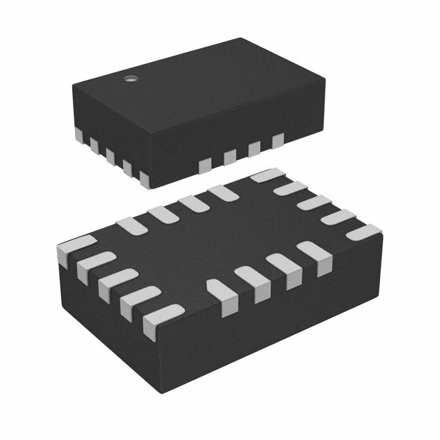
- Part No.:
- MP5092GD-P
- Manufacturer:
- Monolithic Power Systems Inc.
- Package:
- 18-VFQFN
- Datasheet:
-
 MP5092GD-P.pdf
- Description:
- IC PWR SWITCH P-CHAN 1:1 18QFN
- Quantity:
- Payment:

- Shipping:

Inventory:486
Please send an inquiry. Send us your inquiry, and we will respond immediately.
Product details
Overview
MP5092GD-P from Monolithic Power Systems is a dual-channel programmable current load switch IC designed for high-efficiency power path control in portable electronics. It integrates two independent 7.5A, low-RDSON (10mΩ @ 5V) FETs, supports 0.5V–5.5V input range, features adjustable soft-start via external capacitor, output discharge function, and thermal shutdown. Used in notebook and tablet power rail sequencing to suppress inrush current and protect downstream circuitry.
For engineers reviewing the MP5092GD-P datasheet, MP5092GD-P pinout, MP5092GD-P application, or MP5092GD-P equivalent, key selection criteria include programmable 7.5A current limiting via ILIM resistor, <200ns short-circuit response, dual-channel enable independence, QFN-18 (2mm×3mm) thermal performance, and output discharge resistance of 200Ω.
Technical Context
The MP5092GD-P implements two fully independent load switch channels, each with dedicated EN, ILIM, SS, VCC, VIN, and VOUT pins-enabling asymmetric configuration and staggered power-up. Its sense-FET current-limit architecture delivers ±6% accuracy at 7.5A (RLIM = 10.5kΩ) and responds within ~20µs to overcurrent events before triggering fast-off protection at ~13A.
Each channel employs an internal 9µA constant-current source charging an external SS capacitor to control slew rate; output voltage rises at 3× the SS pin ramp rate. Thermal shutdown activates at 155°C with 30°C hysteresis, and output discharge engages automatically when EN is deasserted under light-load conditions via a 200Ω internal pulldown.
Key Specifications
| Parameter | Value and Actual Design Meaning |
|---|---|
| Max Continuous Current per Channel | 7.5A - supports USB-C PD, SSD, and display power rails without external FETs |
| RDSON (Typ, VCC = 5V) | 10mΩ - minimizes conduction loss (<380mW at 7.5A), enabling compact thermal design |
| Input Voltage Range | 0.5V to 5.5V - compatible with single-cell Li-ion (2.7–4.2V), LDO outputs, and 3.3V/5V system rails |
| Soft-Start Response Time | Configurable via SS capacitor (e.g., 100nF → ~20ms) - prevents backplane voltage droop during hot-swap insertion |
| Short-Circuit Response | <200ns - limits peak fault current to ~13A, protecting upstream converters and PCB traces |
| Shutdown Quiescent Current | <1µA - preserves battery life in always-on standby modes of portable devices |
| Output Discharge Resistance | 200Ω - discharges 100µF load in ~22ms (τ = R×C), meeting USB PD quick-turnoff requirements |
Pinout & Package
MP5092GD-P is housed in a thermally enhanced 18-pin QFN package measuring 2mm × 3mm with exposed thermal pad. The package supports high-density layout and efficient heat dissipation in space-constrained mobile applications.
| Pin/Terminal | Circuit Role | Design Meaning |
|---|---|---|
| VIN1, VIN2 (Pins 1,4,10,13) | Channel Input Power Supply | Accepts separate 0.5–5.5V inputs per channel; enables rail isolation and mixed-voltage domain control |
| VOUT1, VOUT2 (Pins 2,3,11,12) | Channel Output to Load | Delivers regulated power to downstream loads; includes integrated 200Ω discharge path when disabled |
| EN1, EN2 (Pins 5,14) | Independent Enable Inputs | CMOS-compatible logic control (1.3–1.7V threshold); allows staggered power-up and dynamic rail management |
| ILIM1, ILIM2 (Pins 8,17) | Current Limit Programming | Resistor-to-ground sets precise 1.5–7.5A limit per channel using ILIM = 82kΩ/RLIM |
| SS1, SS2 (Pins 9,18) | Soft-Start Timing Control | 9µA internal current source charges external capacitor; defines controlled VOUT slew rate (3× SS ramp) |
| VCC1, VCC2 (Pins 7,16) | Control Circuit Bias Supply | 3–5.5V supply for gate drivers and sensing; can be tied to VIN if ≥3V, reducing BOM count |
| GND (Pins 6,15) | Power and Signal Ground | Dual ground pins minimize ground bounce and improve current-sense accuracy across both channels |
Key Features
| Feature | Design Value |
|---|---|
| Dual independent 7.5A load switches | Enables concurrent or sequenced power delivery to multiple subsystems (e.g., CPU core + GPU rail) without cross-talk |
| Programmable current limit (1.5–7.5A) | External resistor sets precise trip point per channel, eliminating need for discrete current-sense amplifiers and comparators |
| Integrated 200Ω output discharge | Automatically drains residual charge from load capacitance upon disable, satisfying USB PD and PCIe hot-plug safety requirements |
| <200ns short-circuit protection | Hardware-fast-off circuit clamps fault current before controller loop reacts, preventing MOSFET avalanche failure |
| QFN-18 (2mm×3mm) with exposed pad | Reduces PCB area by >40% vs. SOIC-8 alternatives while delivering 1.8W power dissipation capability (θJA = 70°C/W) |
Applications
| Notebook Power Rail Management | Tablet Display Backlight Control |
|---|---|
Use Scenario: Sequencing 3.3V and 5V rails powering CPU cores, memory, and I/O in ultrabook platforms with strict inrush limits. IC Role / Device Role / Timing Role: Dual-channel load switch providing independent enable timing, programmable current limiting, and soft-start to prevent system brownout during boot. Use Value: Eliminates need for discrete FETs, gate drivers, and current-sense resistors-reducing BOM count by 7 components per rail and saving 12mm² PCB area. | Use Scenario: Driving LED backlight arrays requiring rapid on/off cycling and safe discharge between frames in 10-inch tablets. IC Role / Device Role / Timing Role: Load switch managing power to boost converter input; output discharge ensures zero-voltage turn-off to avoid LED ghosting. Use Value: 200Ω discharge path clears 100µF capacitive load in <25ms, meeting MIPI DSI frame-sync timing constraints without added circuitry. |
| USB-C Power Delivery Sink | Portable SSD Power Sequencing |
Use Scenario: Controlling VBUS power delivery to USB-C peripheral ports with overcurrent protection and hot-plug compliance. IC Role / Device Role / Timing Role: Dual-channel switch isolating VCONN and VBUS paths; independent ILIM programming enforces USB PD spec current limits (3A/5A). Use Value: Meets USB PD 3.1 sink-side fault response time (<100µs) via hardware-fast-off, avoiding firmware-dependent protection delays. | Use Scenario: Enabling NVMe SSD power rails (1.8V, 3.3V) with controlled ramp-up to prevent NAND flash initialization failures due to voltage overshoot. IC Role / Device Role / Timing Role: Dual-channel load switch with matched soft-start timing across rails to ensure proper power-up sequence per JEDEC specification. Use Value: Adjustable SS capacitor (e.g., 47nF → 9ms) synchronizes rail rise times within ±5%, eliminating reset glitches during cold start. |
Equivalent & Alternatives
The following parts are listed as comparable options for similar dual-channel programmable load switch applications.
| Alternative Part | Technical Difference | Application Difference | Selection Advice |
|---|---|---|---|
| TI TPS22992 | Single-channel, 6A max, fixed 12mΩ RDSON, no output discharge | Lacks dual-channel independence and discharge function; requires two devices for MP5092GD-P's functionality | Select when only one rail needs protection and board space permits duplication |
| ON Semi NCP45561 | Dual-channel, 6A/channel, 15mΩ RDSON, programmable OCP but no soft-start or discharge | Higher conduction loss (+50%), no slew-rate control or automatic discharge-requires external circuitry for USB PD compliance | Choose for cost-sensitive designs where thermal margin exists and discharge is handled externally |
Compared with TPS22992 and NCP45561, MP5092GD-P uniquely integrates dual 7.5A channels, 10mΩ RDSON, programmable soft-start, and 200Ω output discharge in a single 2mm×3mm package-delivering full USB PD sink and notebook rail-management capability without supplemental components.
Availability
MP5092GD-P is available at Aetrix Electronics and suitable for notebook power sequencing, tablet display backlight control, USB-C PD sink implementation, and portable SSD power management requiring stable component supply and long-term industrial availability.
Supply support for MP5092GD-P includes scheduled delivery planning, volume procurement assistance, BOM continuity management, traceable sourcing, and lifecycle availability coordination for OEM customers, industrial embedded developers, connected-device designers, and electronics production programs.
Manufacturer
Monolithic Power Systems (MPS) is a fabless semiconductor company specializing in high-performance analog and power ICs, with design centers in the US, China, and Taiwan, and global manufacturing partnerships.
The MP5092GD-P belongs to MPS's load switch product line, engineered specifically for space-constrained, high-current portable electronics requiring precision current limiting, ultrafast fault response, and integrated discharge-addressing thermal, size, and reliability challenges in modern mobile platforms.
FAQ
What is the minimum input voltage required for MP5092GD-P to operate?
The MP5092GD-P supports an input voltage range from 0.5V to 5.5V per channel. Operation below 0.5V is not guaranteed, as the internal UVLO circuit disables the device when VIN drops below its 0.5V threshold. This enables compatibility with partially discharged Li-ion cells and low-voltage auxiliary rails.
How is the 7.5A current limit set, and what resistor value is required?
The 7.5A current limit is set using an external resistor from ILIM1 or ILIM2 to GND. Per the formula ILIM = 82 kΩ / RLIM, a 10.5 kΩ resistor yields 7.5A (82,000 ÷ 10,500 ≈ 7.5). Resistor tolerance directly impacts accuracy-1% metal-film resistors are recommended for ±1% current limit variation.
Does MP5092GD-P require separate VCC supplies for each channel?
No-VCC1 and VCC2 can be tied together and supplied from a common 3–5.5V bias rail. Each channel's control circuitry operates independently, but sharing VCC reduces component count. If VIN ≥ 3V, VCC may be directly connected to VIN, eliminating the need for a dedicated bias supply.
What happens during a short-circuit event, and how does recovery work?
Upon short-circuit detection (>13A), the MP5092GD-P triggers hardware-fast-off within <200ns, disabling the FET for 80µs. After this blanking period, it attempts auto-recovery by re-enabling the channel. If the fault persists, it cycles between off and retry until cleared-preventing latch-up while maintaining system visibility.
Can MP5092GD-P be used with output capacitances larger than 1000µF?
Yes-but large output capacitance increases inrush current duration. When VOUT rise exceeds the soft-start window, the current limit engages, extending effective startup time. For >1000µF loads, increase SS capacitor value (e.g., 220nF) and verify thermal margin, as sustained current limiting raises junction temperature.
Is the output discharge function active for both channels simultaneously?
Yes-the discharge path (200Ω internal pulldown) activates independently on each channel when its respective EN pin is driven low. Discharge occurs only when the load is lightly loaded (no significant sink current); heavy loads discharge through their own path, and the internal resistor remains inactive.
What PCB layout practices are critical for thermal performance?
Thermal performance depends on soldering the exposed thermal pad to a minimum 100mm² copper pour with ≥6 thermal vias (0.3mm diameter) to inner ground planes. Place ILIM and SS capacitors within 2mm of their pins, and route high-current VIN/VOUT traces with ≥15mil width to limit IR drop and heating.
MP5092GD-P Specifications
- Product attributes
- Attribute value
- Manufacturer:
- Monolithic Power Systems Inc.
- Package/Case:
- 18-VFQFN
- Series:
- -
- Packaging:
- Tape & Reel (TR)
- Product Status:
- Active
- Switch Type:
- General Purpose
- Number of Outputs:
- 2
- Ratio - Input:Output:
- 1:1
- Output Configuration:
- High Side
- Output Type:
- P-Channel
- Interface:
- On/Off
- Voltage - Load:
- 3V ~ 5.5V
- Voltage - Supply (Vcc/Vdd):
- Not Required
- Current - Output (Max):
- 7.5A
- Rds On (Typ):
- 10mOhm
- Input Type:
- Non-Inverting
- Features:
- Load Discharge, Slew Rate Controlled
- Fault Protection:
- Current Limiting (Adjustable), Over Temperature
- Operating Temperature:
- -40°C ~ 125°C (TJ)
- Grade:
- -
- Qualification:
- -
- Mounting Type:
- Surface Mount
- Supplier Device Package:
- 18-QFN (2x3)
MP5092GD-P FAQ
1.How can I place an order for MP5092GD-P through Aetrix?
Please submit a Request for Quotation (RFQ) for MP5092GD-P on Aetrix. Our sales agent will provide a competitive quotation and guide you through the order confirmation once you accept the terms.
2.Are the price and stock information for MP5092GD-P reliable?
The price and inventory of MP5092GD-P are updated periodically and may fluctuate due to market conditions. Stock and pricing data are typically refreshed every 24 hours. Quotation validity for MP5092GD-P is usually 5 days.
3.What payment methods are accepted for MP5092GD-P?
We accept Wire Transfer, PayPal, Credit Card, Western Union, MoneyGram, and Escrow for MP5092GD-P transactions.
Note: Certain payment methods may incur a processing fee.
4.How is shipping managed for MP5092GD-P?
MP5092GD-P orders can be shipped via leading logistics carriers, including DHL, UPS, FedEx, TNT, or Registered Mail.
Once your MP5092GD-P order is processed, you will receive an email with the shipment details and tracking number.
Note: Tracking information may take up to 24 hours to appear. Express delivery typically takes 3–5 business days.
5.How can I obtain technical support or documentation for MP5092GD-P?
For technical support, including MP5092GD-P datasheets, pinout diagrams, or application guidance, please contact our engineering support team. They can provide detailed documentation and assistance for your MP5092GD-P requirements.
6.How does Aetrix verify that MP5092GD-P is sourced from the original manufacturer or authorized distributors?
All MP5092GD-P products on Aetrix are procured from qualified distributors and authorized channels. Our dedicated quality assurance team conducts strict verification, including traceability checks and, if necessary, third-party testing. This ensures that MP5092GD-P meets industry standards.
7.What is the process for return or replacement of MP5092GD-P?
All MP5092GD-P units undergo pre-shipment inspection (PSI). If there is an issue with MP5092GD-P, returns or replacements are accepted under the following conditions:
1.Quantity discrepancies, incorrect items, or visible external defects (such as breakage or corrosion), acknowledged by Aetrix.
2.The issue is reported within 90 days of delivery.
3.The MP5092GD-P part is unused and in its original packaging.
Return procedure for MP5092GD-P:
1.Submit a request within 90 days.
2.Obtain a Return Material Authorization (RMA) from Aetrix.
MP5092GD-P Tags

-
TPS22919DCKR
Texas Instruments

-
MIC2091-1YM5-TR
Microchip Technology

-
MIC2090-1YM5-TR
Microchip Technology

-
TPS22995RZFR
Texas Instruments

-
TPS22975DSGR
Texas Instruments

-
SIP32510DT-T1-GE3
Vishay Siliconix

-
ULN2003D1013TR
STMicroelectronics

-
MIC2005A-1YM5-TR
Microchip Technology

-
MIC2005A-1YM6-TR
Microchip Technology

-
TPS22916BYFPR
Texas Instruments

-
TPS22917DBVR
Texas Instruments

-
ULN2003APWR
Texas Instruments
Tech Hub

Operational amplifier guide covering op amp basics, feedback, ideal vs real op amps, common configurations, buffer circuits, offset, bias current, gain-bandwidth, slew rate, rail-to-rail limits and sel…

Jumper cables guide covering safe connection order, red and black clamp placement, final ground connection, cable gauge, length, clamp quality, copper vs CCA cables, jump starter comparison and battery…

LDO regulator guide covering low dropout voltage, power dissipation, thermal design, PSRR, output noise, capacitor stability, adjustable LDO circuits, LDO vs buck converter and datasheet selection chec…

Conditional Access Module guide covering CAM meaning, CI/CI+ interface, smart card authorization, DVB security workflow, TV and set-top box compatibility, internal electronics, ESD protection, connecto…

Guide to electronic component obsolescence covering EOL risk, PCN/PDN notices, last-time buy planning, replacement options, form-fit-function validation, counterfeit risk and BOM lifecycle management.

18650 battery guide covering lithium-ion cell basics, 3.6V/3.7V voltage, 4.2V charging, mAh and Wh capacity, protected cells, chargers, BMS, series-parallel packs, holders, welding and sourcing checks.…

Hall effect sensor guide covering working principle, linear and digital sensors, Arduino circuits, current sensing, speed detection, automotive applications, A3144 examples, signal filtering and datash…

Product Change Notification guide for electronic components, covering PCN meaning, PCN vs PDN/EOL, common change types, risk levels, form-fit-function review, engineering validation, BOM control, LTB/L…

A practical guide to blend door actuators, covering HVAC function, symptoms, location, AC and heater issues, reset and calibration, replacement cost, electrical diagnosis, compatibility checks, and rep…

Engineering guide to Raspberry Pi alternatives, covering chip-level differences, Orange Pi, ROCK, Jetson, Banana Pi, NanoPi, Compute Module, Pico, GPIO, camera, HAT compatibility, and replacement risks…


