
 My Inquiry
 My Account


Monolithic Power Systems Inc. MP5610GQG-Z
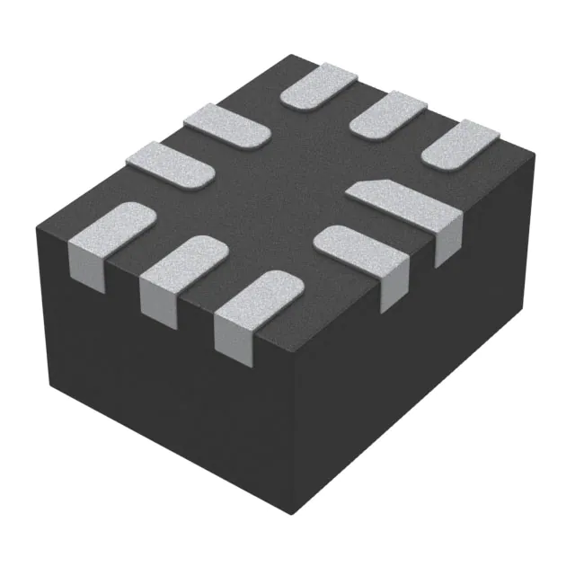
- Part No.:
- MP5610GQG-Z
- Manufacturer:
- Monolithic Power Systems Inc.
- Category:
- Special Purpose Regulators
- Package:
- 10-VFQFN
- Datasheet:
-
 MP5610GQG-Z.pdf
- Description:
- IC REG CONV LCD 2OUT 10QFN
- Quantity:
- Payment:

- Shipping:

Inventory:1,644
Please send an inquiry. Send us your inquiry, and we will respond immediately.
Product details
Overview
MP5610GQG-Z from Monolithic Power Systems is a dual-channel LCD bias power supply IC integrating a 1.2MHz peak-current-mode step-up converter and a negative charge pump, delivering ±5.4V at up to 50mA per rail from a 2.7V–5.5V input. It features 0.5% line/load regulation, 1% voltage tracking between outputs, and internal synchronous rectification for high efficiency in space-constrained displays.
For engineers reviewing the MP5610GQG-Z datasheet, MP5610GQG-Z pinout, MP5610GQG-Z application, or MP5610GQG-Z equivalent, this device is selected for compact LCD bias generation requiring precise dual-rail tracking, low quiescent current (500μA), robust protection (OVP/UVP/OTP/UVLO), and QFN-10 (1.4mm×1.8mm) footprint compatibility.
Technical Context
The MP5610GQG-Z implements a peak-current-mode controlled boost converter for VOP regulation and a charge-pump topology for VON generation, where energy is drawn directly from the SW node-eliminating a separate input path and improving system efficiency. Its voltage tracking is actively maintained via closed-loop adjustment of PMOS M6's on-resistance based on the sum of VOP and VON.
Protection architecture includes cycle-by-cycle current limiting (240–365mA), input DC current limit (200–290mA), output overvoltage thresholds (VOP_OVP = 6.1V, VON_OVP = −6.2V), under-voltage latching (VUVP_P = 52%×VREF, VUVP_N = 60%×VOP), and thermal shutdown at 150°C. Soft-start time is fixed at 270μs with linear reference ramping.
Key Specifications
| Parameter | Value and Actual Design Meaning |
|---|---|
| Input Voltage Range | 2.7V to 5.5V - supports single-cell Li-ion, Li-polymer, or 3.3V/5V rail inputs without external LDO pre-regulation. |
| Switching Frequency | 1.2MHz (±20%) - enables use of small 10μH inductors and <5μF ceramic capacitors for minimal PCB area. |
| Max Output Current | 50mA per rail - sufficient for biasing small-to-midsize segment LCDs (e.g., feature phone panels, smartwatch displays). |
| Voltage Tracking Error | ±1% - ensures matched positive/negative rail magnitudes critical for LCD contrast stability and reduced image ghosting. |
| Feedback Reference | 600mV ±1% - sets precise output via external resistor divider; enables programmable VOP up to +5.8V. |
| Quiescent Current | 500μA - minimizes standby power draw in battery-powered portable devices during display sleep modes. |
| Thermal Shutdown | 150°C junction - protects against sustained overload or poor heatsinking in sealed enclosures. |
Pinout & Package
MP5610GQG-Z is housed in a thermally enhanced QFN-10 package (1.4mm × 1.8mm, 0.5mm pitch) with exposed thermal pad. Pin 1 is marked by a dot; top-side marking is "BZ".
| Pin/Terminal | Circuit Role | Design Meaning |
|---|---|---|
| 1 EN | Enable control input | Active-high logic enable (1.2V threshold); internal 1MΩ pulldown ensures safe default disable state. |
| 2 FBP | Positive output feedback | Connects to resistor divider midpoint; 600mV reference sets VOP with ±1% accuracy. |
| 3 VON | Negative output terminal | Delivers regulated negative rail (e.g., −5.4V); requires local 2.2μF ceramic bypass capacitor. |
| 4 CP2 | Charge pump flying node 2 | Connects to one side of flying capacitor (CP1–CP2); switches synchronously with SW and VOP rectifier. |
| 5 CP1 | Charge pump flying node 1 | Connects to other side of flying capacitor; forms energy transfer path from SW node to VON. |
| 6 GND | Power and signal ground | Common return for all circuits; must be low-impedance and tied directly to thermal pad. |
| 7 VOP | Positive output terminal | Delivers regulated positive rail (e.g., +5.4V); requires local 2.2μF ceramic bypass capacitor. |
| 8 SW | Boost switch node | Drain of internal low-side MOSFET; connects to inductor; carries high di/dt switching current. |
| 9 VINP | Boost stage input | Supplies power to boost power stage only; internally connected to source of N-MOSFET M1. |
| 10 VIN | Main supply input | Powers internal logic, gate drivers, and bias circuitry; must be locally bypassed with ≥1μF ceramic capacitor. |
Key Features
| Feature | Design Value |
|---|---|
| Dual-rail tracking control | Active closed-loop adjustment of PMOS M6 on-resistance maintains |VON|/VOP ratio within ±1%, critical for LCD gamma consistency. |
| Integrated synchronous rectification | Eliminates external Schottky diode; reduces conduction loss and thermal stress while shrinking solution size. |
| Direct-switch-node charge pump | Draws energy from SW node instead of VIN, avoiding extra conversion loss and improving overall efficiency by ~8–12% vs. independent pumps. |
| Comprehensive fault protection | Includes latch-off UVP/OVP on both rails, input UVLO with 260mV hysteresis, cycle-by-cycle current limit, and thermal shutdown. |
| Low-noise soft-start | 270μs linear reference ramp prevents inrush current and ensures monotonic VOP/VON startup with zero-crossing tracking. |
Applications
| Smartphone LCD Bias | Feature Phone Display Supply |
|---|---|
|
Use Scenario: Powering segment-based LCDs in entry-level smartphones with limited board area and battery capacity. IC Role / Device Role / Timing Role: Dual-rail bias generator providing matched ±5.4V rails from single 3.7V Li-ion cell. Use Value: 1% voltage tracking eliminates contrast drift across temperature; QFN-10 footprint saves >30% PCB area vs. discrete solutions. |
Use Scenario: Supplying bias voltage for monochrome STN/TN LCDs in cost-sensitive feature phones. IC Role / Device Role / Timing Role: Integrated step-up + charge pump replaces two discrete DC/DC converters and external diodes. Use Value: 500μA quiescent current extends standby time; input UVLO prevents brownout operation below 2.45V. |
| Wearable Display Module | Industrial Handheld Terminal |
|
Use Scenario: Driving small OLED or reflective LCD panels in smartwatches and fitness trackers. IC Role / Device Role / Timing Role: Compact dual-output supply enabling ultra-thin form factors with tight thermal constraints. Use Value: 150°C thermal shutdown protects against enclosure overheating; 1.2MHz switching allows <1mm² inductor placement. |
Use Scenario: Providing stable LCD bias in ruggedized handheld terminals operating across −40°C to +85°C ambient. IC Role / Device Role / Timing Role: Robust bias IC with latch-off UVP/OVP and wide input range (2.7–5.5V) for variable battery states. Use Value: −40°C to +125°C junction rating ensures reliability in uncontrolled environments; RoHS/halogen-free compliance meets industrial standards. |
Equivalent & Alternatives
The following parts are listed as comparable options for similar dual-output LCD bias power supply applications.
| Alternative Part | Technical Difference | Application Difference | Selection Advice |
|---|---|---|---|
| TPS65136RGTR | Fixed +5.0V/−5.0V outputs; no programmability; uses external diode rectification; larger 3mm×3mm QFN-16 package. | Lacks voltage tracking control; less suitable for gamma-critical displays requiring tight rail matching. | Prefer when fixed outputs suffice and board space is not constrained; avoid if programmable VOP or <1% tracking required. |
| RT9048AGQW | 1.5MHz switching; max 40mA per rail; no integrated synchronous rectifier; higher 1.2V feedback reference. | Lower output current limits performance in higher-resolution segment LCDs; reduced efficiency due to diode losses. | Select only for lower-power monochrome panels; verify thermal margin at full load due to lack of sync rectification. |
Compared with TPS65136RGTR and RT9048AGQW, MP5610GQG-Z delivers superior voltage tracking (±1% vs. ±3–5%), higher output current (50mA vs. 40mA), smaller footprint (1.4mm×1.8mm vs. 3mm×3mm/2mm×2mm), and integrated synchronous rectification-making it optimal for space- and precision-constrained portable LCD systems.
Availability
MP5610GQG-Z is available at Aetrix Electronics and suitable for smartphone LCD bias, feature phone display supply, wearable display modules, and industrial handheld terminals requiring stable component supply across extended temperature ranges and long production lifecycles.
Supply support for MP5610GQG-Z includes scheduled delivery planning, volume procurement assistance, BOM continuity management, traceable sourcing, and lifecycle availability coordination for OEM customers, industrial embedded developers, connected-device designers, and electronics production programs.
Manufacturer
Monolithic Power Systems (MPS) is a fabless semiconductor company specializing in high-performance analog and power ICs, with design centers in the US, China, and Taiwan, and global manufacturing partnerships.
The MP5610 belongs to MPS's LCD bias power supply product line, engineered specifically for compact, high-efficiency dual-rail generation in portable consumer displays-emphasizing tracking accuracy, thermal resilience, and minimal external component count.
FAQ
What is the maximum achievable positive output voltage with MP5610GQG-Z?
The MP5610GQG-Z supports programmable positive output voltage up to +5.8V using an external resistor divider on the FBP pin. This is set by the 600mV internal reference and resistor ratio; typical configurations yield +5.4V for standard LCD bias, but scaling beyond that remains within specification limits and validated thermal performance.
How does the MP5610GQG-Z achieve voltage tracking between VOP and VON?
Voltage tracking is achieved through closed-loop control of PMOS M6's on-resistance, which adjusts dynamically based on the sum of VOP and VON. If the sum deviates from zero, the gate driver modifies M6's resistance to drop additional voltage, maintaining |VON|/VOP within ±1%. This is implemented entirely on-die with no external components required.
Can MP5610GQG-Z operate from a 2.7V input while delivering 50mA on both rails?
Yes-MP5610GQG-Z is fully specified down to 2.7V input and delivers up to 50mA per rail across its full input range. At 2.7V, efficiency drops modestly (~78% at full load), but all protections (current limit, thermal, OVP/UVP) remain active and functional per datasheet test conditions.
Is the EN pin internally pulled down, and what is its threshold behavior?
Yes, the EN pin has an internal 1MΩ pull-down resistor to GND. The enable threshold is 1.2V (typical) with hysteresis: rising-edge activation occurs at ~1.2V, and falling-edge disable occurs at ~0.4V. This ensures noise immunity and predictable startup/shutdown sequencing without external components.
What is the recommended flying capacitor value and dielectric type for CP1–CP2?
MPS recommends a 0.47μF X7R ceramic capacitor between CP1 and CP2, rated for ≥10V DC. X7R dielectric ensures stable capacitance across temperature and bias voltage; values from 0.1μF to 1μF are acceptable depending on load transient requirements and EMI targets, per Section 9.3 of the datasheet.
Does MP5610GQG-Z require external compensation components for loop stability?
No-MP5610GQG-Z uses internal compensation optimized for standard 10μH inductors and 2.2μF output capacitors. The control loop is factory-tuned for stability across all operating conditions; no external compensation network is needed or supported in the reference design.
How does the input disconnect MOSFET (M5) function during startup?
M5 is an internal NMOS switch between VIN and VINP. During startup, its gate drive ramps gradually over ~215μs, limiting inrush current into the boost stage. This prevents input voltage sag and ensures synchronized, zero-crossing startup of VOP and VON-critical for LCD panel initialization integrity.
MP5610GQG-Z Specifications
- Product attributes
- Attribute value
- Manufacturer:
- Monolithic Power Systems Inc.
- Series:
- -
- Package/Case:
- 10-VFQFN
- Packaging:
- Tape & Reel (TR)
- Product Status:
- Active
- Applications:
- Converter, LCD
- Voltage - Input:
- 2.7V ~ 5.5V
- Number of Outputs:
- 2
- Voltage - Output:
- Programmable
- Operating Temperature:
- -40°C ~ 125°C
- Grade:
- -
- Qualification:
- -
- Mounting Type:
- Surface Mount
- Supplier Device Package:
- 10-QFN (1.4x1.8)
MP5610GQG-Z FAQ
1.How can I place an order for MP5610GQG-Z through Aetrix?
Please submit a Request for Quotation (RFQ) for MP5610GQG-Z on Aetrix. Our sales agent will provide a competitive quotation and guide you through the order confirmation once you accept the terms.
2.Are the price and stock information for MP5610GQG-Z reliable?
The price and inventory of MP5610GQG-Z are updated periodically and may fluctuate due to market conditions. Stock and pricing data are typically refreshed every 24 hours. Quotation validity for MP5610GQG-Z is usually 5 days.
3.What payment methods are accepted for MP5610GQG-Z?
We accept Wire Transfer, PayPal, Credit Card, Western Union, MoneyGram, and Escrow for MP5610GQG-Z transactions.
Note: Certain payment methods may incur a processing fee.
4.How is shipping managed for MP5610GQG-Z?
MP5610GQG-Z orders can be shipped via leading logistics carriers, including DHL, UPS, FedEx, TNT, or Registered Mail.
Once your MP5610GQG-Z order is processed, you will receive an email with the shipment details and tracking number.
Note: Tracking information may take up to 24 hours to appear. Express delivery typically takes 3–5 business days.
5.How can I obtain technical support or documentation for MP5610GQG-Z?
For technical support, including MP5610GQG-Z datasheets, pinout diagrams, or application guidance, please contact our engineering support team. They can provide detailed documentation and assistance for your MP5610GQG-Z requirements.
6.How does Aetrix verify that MP5610GQG-Z is sourced from the original manufacturer or authorized distributors?
All MP5610GQG-Z products on Aetrix are procured from qualified distributors and authorized channels. Our dedicated quality assurance team conducts strict verification, including traceability checks and, if necessary, third-party testing. This ensures that MP5610GQG-Z meets industry standards.
7.What is the process for return or replacement of MP5610GQG-Z?
All MP5610GQG-Z units undergo pre-shipment inspection (PSI). If there is an issue with MP5610GQG-Z, returns or replacements are accepted under the following conditions:
1.Quantity discrepancies, incorrect items, or visible external defects (such as breakage or corrosion), acknowledged by Aetrix.
2.The issue is reported within 90 days of delivery.
3.The MP5610GQG-Z part is unused and in its original packaging.
Return procedure for MP5610GQG-Z:
1.Submit a request within 90 days.
2.Obtain a Return Material Authorization (RMA) from Aetrix.
MP5610GQG-Z Tags

-
TPS51206DSQR
Texas Instruments

-
TPS51200DRCR
Texas Instruments
-
TPS51200DRCT
Texas Instruments

-
TPS62740DSSR
Texas Instruments

-
TPS51100DGQR
Texas Instruments

-
NCP51200MNTXG
onsemi
-
NCP51400MNTXG
onsemi

-
RT9026GSP
Richtek USA Inc.

-
LP2998MRX/NOPB
Texas Instruments
-
TPS51200QDRCRQ1
Texas Instruments

-
DPA423GN-TL
Power Integrations
-
LM10011SD/NOPB
Texas Instruments
Tech Hub

Operational amplifier guide covering op amp basics, feedback, ideal vs real op amps, common configurations, buffer circuits, offset, bias current, gain-bandwidth, slew rate, rail-to-rail limits and sel…

Jumper cables guide covering safe connection order, red and black clamp placement, final ground connection, cable gauge, length, clamp quality, copper vs CCA cables, jump starter comparison and battery…

LDO regulator guide covering low dropout voltage, power dissipation, thermal design, PSRR, output noise, capacitor stability, adjustable LDO circuits, LDO vs buck converter and datasheet selection chec…

Conditional Access Module guide covering CAM meaning, CI/CI+ interface, smart card authorization, DVB security workflow, TV and set-top box compatibility, internal electronics, ESD protection, connecto…

Guide to electronic component obsolescence covering EOL risk, PCN/PDN notices, last-time buy planning, replacement options, form-fit-function validation, counterfeit risk and BOM lifecycle management.

18650 battery guide covering lithium-ion cell basics, 3.6V/3.7V voltage, 4.2V charging, mAh and Wh capacity, protected cells, chargers, BMS, series-parallel packs, holders, welding and sourcing checks.…

Hall effect sensor guide covering working principle, linear and digital sensors, Arduino circuits, current sensing, speed detection, automotive applications, A3144 examples, signal filtering and datash…

Product Change Notification guide for electronic components, covering PCN meaning, PCN vs PDN/EOL, common change types, risk levels, form-fit-function review, engineering validation, BOM control, LTB/L…

A practical guide to blend door actuators, covering HVAC function, symptoms, location, AC and heater issues, reset and calibration, replacement cost, electrical diagnosis, compatibility checks, and rep…

Engineering guide to Raspberry Pi alternatives, covering chip-level differences, Orange Pi, ROCK, Jetson, Banana Pi, NanoPi, Compute Module, Pico, GPIO, camera, HAT compatibility, and replacement risks…


