
 My Inquiry
 My Account


Monolithic Power Systems Inc. MP6401DGT-33AD3-LF-P
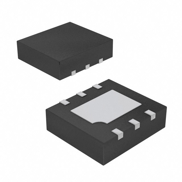
- Part No.:
- MP6401DGT-33AD3-LF-P
- Manufacturer:
- Monolithic Power Systems Inc.
- Package:
- 6-WDFN Exposed Pad
- Datasheet:
-
 MP6401DGT-33AD3-LF-P.pdf
- Description:
- IC REG LINEAR 3.3V 300MA 6TQFN
- Quantity:
- Payment:

- Shipping:

Inventory:3,908
Please send an inquiry. Send us your inquiry, and we will respond immediately.
Product details
Overview
MP6401DGT-33AD3-LF-P from Monolithic Power Systems is a 300mA low-dropout linear regulator with integrated push-pull active-low reset circuit, fixed 3.3V output (±2% accuracy), -7.5% reset threshold, and 200ms reset delay. It operates from 2.5V–5.5V input, delivers 114mV dropout at full load, and targets space-constrained portable electronics requiring regulated power and reliable microprocessor supervision.
For engineers reviewing the MP6401DGT-33AD3-LF-P datasheet, MP6401DGT-33AD3-LF-P pinout, MP6401DGT-33AD3-LF-P application, or MP6401DGT-33AD3-LF-P equivalent, this device serves as a single-chip solution for voltage regulation and power-on reset in battery-powered smart phones, GPS modules, and wireless edge devices where quiescent current (80μA), noise (15μVRMS), and thermal protection are critical selection criteria.
Technical Context
The MP6401 integrates an LDO regulator core with a dedicated reset comparator monitoring the OUT pin against a precision internal reference. Its reset logic asserts when VOUT falls below 92.5% of nominal (–7.5% threshold) and deasserts after a factory-programmed 200ms delay, independent of EN state once triggered.
Regulation uses an internal error amplifier driving a PMOS pass element with reverse-current protection, thermal shutdown (150°C trip), and current limiting (500mA). The ADJ pin enables either fixed-output mode (GND-connected) or adjustable mode (resistor-divider feedback), with 1.229V reference voltage and ±2% output accuracy over –40°C to +85°C.
Key Specifications
| Parameter | Value and Actual Design Meaning |
|---|---|
| Output Voltage | Fixed 3.3V ±2% - ensures stable supply for 3.3V I/O domains and microcontrollers without external feedback components. |
| Max Output Current | 300mA continuous - supports moderate-power baseband processors, RF transceivers, and sensor subsystems in portable designs. |
| Dropout Voltage | 114mV at 300mA - enables operation down to 3.414V input while maintaining regulation, extending battery runtime in Li-ion and dual-cell alkaline systems. |
| Quiescent Current | 80μA - minimizes standby drain in always-on circuits such as real-time clocks and wake-up supervisors. |
| Reset Threshold | –7.5% of VOUT (92.5% of 3.3V = 3.0525V) - matches standard microprocessor brownout detection levels for clean system initialization. |
| Reset Delay | 200ms typical - provides sufficient hold-off time to allow power rails and clock sources to stabilize before releasing processor reset. |
| PSRR | 57dB at 1kHz - suppresses switching noise from upstream DC/DC converters, preserving signal integrity in analog and RF sections. |
| Output Noise | 15μVRMS (10Hz–100kHz) - meets low-noise requirements for ADC references, audio codecs, and precision sensors. |
Pinout & Package
MP6401DGT-33AD3-LF-P is housed in a 2mm × 2mm TQFN6 package with exposed thermal pad, optimized for compact PCB layouts and efficient heat dissipation in handheld devices.
| Pin/Terminal | Circuit Role | Design Meaning |
|---|---|---|
| 1 - IN | Input supply connection | Accepts 2.5V–5.5V unregulated input; connects directly to battery or DC/DC output; reverse leakage limited to 1μA when VOUT > VIN. |
| 2 - GND | Power ground reference | Common return path for regulator and reset circuitry; must be connected to low-impedance PCB ground plane for thermal and noise performance. |
| 3 - EN | Enable control (active-high) | Logic high (>0.7×VIN) enables regulation; low disables output and reduces IQ to 0.1μA; must not be left floating. |
| 4 - OUT | Regulated output | Delivers 3.3V ±2% at up to 300mA; requires ≥3.3μF ceramic capacitor (X5R/X7R) on board for stability. |
| 5 - ADJ | Mode selection / feedback node | Connected to GND for fixed 3.3V output; open or pulled to GND via ≤50kΩ for guaranteed fixed-mode operation. |
| 6 - RESET | Push-pull active-low reset output | Drives low (≤0.4V @ 3.2mA) when VOUT drops below threshold; drives high (≥0.8×VOUT) when valid; no external pull-up required. |
Key Features
| Feature | Design Value |
|---|---|
| Integrated reset function | Eliminates need for discrete supervisor IC, reducing BOM count and PCB area in space-limited portable designs. |
| Ultra-low noise output | 15μVRMS enables direct powering of noise-sensitive analog blocks without additional filtering stages. |
| Thermal and short-circuit protection | Auto-recovering shutdown at 150°C (20°C hysteresis) prevents damage during transient overload or poor heatsinking. |
| Reverse current blocking | Prevents backflow from VOUT to VIN during input removal, enabling seamless backup battery switchover in memory retention circuits. |
| Low quiescent current | 80μA operation allows use in always-on subsystems without compromising battery shelf life beyond 1 year. |
Applications
| Smartphone Baseband Power | Portable GPS Module |
|---|---|
|
Use Scenario: Regulating main 3.3V rail for cellular modem and GNSS receiver ICs in slim smartphone form factors. IC Role / Device Role / Timing Role: Primary LDO delivering clean 3.3V supply and asserting hardware reset if VOUT sags during RF transmission bursts. Use Value: 114mV dropout preserves regulation during battery voltage sag; 200ms reset delay ensures GNSS cold start completes before processor release. |
Use Scenario: Powering standalone GPS receivers in wearable trackers and asset tags with intermittent satellite visibility. IC Role / Device Role / Timing Role: Stable 3.3V source for GPS baseband ASIC and integrated reset generator for cold/warm restart synchronization. Use Value: 80μA IQ extends battery life in low-duty-cycle tracking; 15μVRMS noise avoids position drift caused by supply-induced timing jitter. |
| Wireless Sensor Node | PDA System Management |
|
Use Scenario: Supplying 3.3V to BLE SoC and environmental sensors in battery-operated industrial IoT nodes. IC Role / Device Role / Timing Role: Single-chip power and reset supervisor ensuring deterministic boot after brownout events induced by RF interference. Use Value: –7.5% reset threshold aligns with BLE SoC reset specs; reverse-current blocking maintains sensor data during battery swap. |
Use Scenario: Providing regulated 3.3V and coordinated reset to PDA application processor and touch controller. IC Role / Device Role / Timing Role: Dual-function regulator/supervisor replacing separate LDO + reset IC, reducing component count in legacy PDA designs. Use Value: TQFN6 footprint saves 40% board area vs. TSOT23-6 alternative; PSRR >57dB suppresses noise from display backlight drivers. |
Equivalent & Alternatives
The following parts are listed as comparable options for similar LDO-with-reset applications.
| Alternative Part | Technical Difference | Application Difference | Selection Advice |
|---|---|---|---|
| TPS79933DRVR | 300mA LDO only; no integrated reset - requires external supervisor (e.g., TPS3808G01) for reset functionality. | Lacks built-in reset timing and threshold control; adds design complexity and board area. | Select when reset behavior must be programmable or when existing designs already use TI ecosystem components. |
| MCP1826-3302E/DB | 300mA LDO with manual reset input but no automatic VOUT monitoring or fixed delay - reset assertion requires external logic. | Cannot autonomously detect brownout; relies on host MCU or external voltage monitor for reset initiation. | Choose when system-level reset coordination is handled by firmware or when cost sensitivity outweighs integration benefit. |
Compared with TPS79933DRVR and MCP1826-3302E/DB, MP6401DGT-33AD3-LF-P uniquely combines fixed 3.3V regulation, autonomous VOUT-monitored reset, and factory-set 200ms delay in one TQFN6 package-reducing bill-of-materials, layout effort, and qualification risk for portable consumer electronics.
Availability
MP6401DGT-33AD3-LF-P is available at Aetrix Electronics and suitable for smartphone baseband power, portable GPS modules, and wireless sensor nodes requiring stable component supply, long-term lifecycle support, and RoHS-compliant packaging.
Supply support for MP6401DGT-33AD3-LF-P includes scheduled delivery planning, volume procurement assistance, BOM continuity management, traceable sourcing, and lifecycle availability coordination for OEM customers, industrial embedded developers, connected-device designers, and electronics production programs.
Manufacturer
Monolithic Power Systems (MPS) is a fabless semiconductor company specializing in high-performance analog and mixed-signal ICs for power management, motion control, and automotive applications.
The MP6401 belongs to MPS's integrated power-supervision LDO product line, designed specifically to replace discrete regulator + supervisor combinations in space- and power-constrained portable electronics.
FAQ
What is the function of the ADJ pin on MP6401DGT-33AD3-LF-P?
The ADJ pin selects operating mode: when tied to GND, it configures the device for fixed 3.3V output; it is not used for feedback in this variant. Leaving ADJ floating or connecting it to high-impedance nodes may cause regulation instability, so a direct GND connection or ≤50kΩ pull-down is mandatory for reliable fixed-voltage operation.
Does MP6401DGT-33AD3-LF-P require an external capacitor on the RESET pin?
No external capacitor is needed on the RESET pin. The 200ms delay is internally generated and factory-trimmed; the push-pull output drives directly into microcontroller reset inputs without pull-up resistors or timing capacitors, simplifying layout and improving noise immunity compared to open-drain reset ICs.
Can MP6401DGT-33AD3-LF-P operate with input voltage below 2.5V?
No. The absolute minimum input voltage is 2.5V per datasheet specifications. Below this, the internal UVLO circuit disables regulation and asserts RESET. Attempting operation at 2.4V or lower will result in unregulated output and undefined reset behavior, risking system malfunction.
How does the reset threshold tolerance affect system reliability?
The –7.5% threshold has ±2.5% tolerance (90–95% of nominal), meaning RESET asserts between 2.97V and 3.135V for a 3.3V output. This ensures robust detection of marginal supply conditions before microprocessor functional failure, while avoiding nuisance resets during brief transients within specification limits.
Is thermal pad soldering required for MP6401DGT-33AD3-LF-P?
Yes. The exposed thermal pad on the TQFN6 package must be soldered to a PCB thermal pad with ≥4 thermal vias to an internal ground plane. Omitting this compromises thermal resistance (θJA rises from 80°C/W to >120°C/W), increasing junction temperature and triggering premature thermal shutdown under 300mA load.
What happens to RESET output during EN pin deactivation?
When EN is pulled low, the regulator shuts down, VOUT collapses, and RESET asserts within 30μs. The RESET output remains asserted as long as EN is low or VOUT remains below threshold - it does not auto-deassert until both EN is high AND VOUT recovers above the threshold for the full 200ms delay period.
Does MP6401DGT-33AD3-LF-P support backup battery operation?
Yes. Its reverse-current protection allows external backup batteries to maintain VOUT during main input removal. When VIN drops, RESET asserts, and the device draws only 40μA from the backup source - sufficient to retain SRAM contents in most microcontrollers without supplemental circuitry.
MP6401DGT-33AD3-LF-P Specifications
- Product attributes
- Attribute value
- Manufacturer:
- Monolithic Power Systems Inc.
- Series:
- -
- Package/Case:
- 6-WDFN Exposed Pad
- Packaging:
- Tape & Reel (TR)
- Product Status:
- Active
- Output Configuration:
- Positive
- Output Type:
- Fixed
- Number of Regulators:
- 1
- Voltage - Input (Max):
- 5.5V
- Voltage - Output (Min/Fixed):
- 3.3V
- Voltage - Output (Max):
- -
- Voltage Dropout (Max):
- 0.22V @ 300mA
- Current - Output:
- 300mA
- Current - Quiescent (Iq):
- 155 µA
- Current - Supply (Max):
- -
- PSRR:
- 57dB (1kHz)
- Control Features:
- Enable
- Protection Features:
- Over Current, Over Temperature, Short Circuit
- Operating Temperature:
- -40°C ~ 125°C
- Grade:
- -
- Qualification:
- -
- Mounting Type:
- Surface Mount
- Supplier Device Package:
- 6-TQFN (2x2)
MP6401DGT-33AD3-LF-P FAQ
1.How can I place an order for MP6401DGT-33AD3-LF-P through Aetrix?
Please submit a Request for Quotation (RFQ) for MP6401DGT-33AD3-LF-P on Aetrix. Our sales agent will provide a competitive quotation and guide you through the order confirmation once you accept the terms.
2.Are the price and stock information for MP6401DGT-33AD3-LF-P reliable?
The price and inventory of MP6401DGT-33AD3-LF-P are updated periodically and may fluctuate due to market conditions. Stock and pricing data are typically refreshed every 24 hours. Quotation validity for MP6401DGT-33AD3-LF-P is usually 5 days.
3.What payment methods are accepted for MP6401DGT-33AD3-LF-P?
We accept Wire Transfer, PayPal, Credit Card, Western Union, MoneyGram, and Escrow for MP6401DGT-33AD3-LF-P transactions.
Note: Certain payment methods may incur a processing fee.
4.How is shipping managed for MP6401DGT-33AD3-LF-P?
MP6401DGT-33AD3-LF-P orders can be shipped via leading logistics carriers, including DHL, UPS, FedEx, TNT, or Registered Mail.
Once your MP6401DGT-33AD3-LF-P order is processed, you will receive an email with the shipment details and tracking number.
Note: Tracking information may take up to 24 hours to appear. Express delivery typically takes 3–5 business days.
5.How can I obtain technical support or documentation for MP6401DGT-33AD3-LF-P?
For technical support, including MP6401DGT-33AD3-LF-P datasheets, pinout diagrams, or application guidance, please contact our engineering support team. They can provide detailed documentation and assistance for your MP6401DGT-33AD3-LF-P requirements.
6.How does Aetrix verify that MP6401DGT-33AD3-LF-P is sourced from the original manufacturer or authorized distributors?
All MP6401DGT-33AD3-LF-P products on Aetrix are procured from qualified distributors and authorized channels. Our dedicated quality assurance team conducts strict verification, including traceability checks and, if necessary, third-party testing. This ensures that MP6401DGT-33AD3-LF-P meets industry standards.
7.What is the process for return or replacement of MP6401DGT-33AD3-LF-P?
All MP6401DGT-33AD3-LF-P units undergo pre-shipment inspection (PSI). If there is an issue with MP6401DGT-33AD3-LF-P, returns or replacements are accepted under the following conditions:
1.Quantity discrepancies, incorrect items, or visible external defects (such as breakage or corrosion), acknowledged by Aetrix.
2.The issue is reported within 90 days of delivery.
3.The MP6401DGT-33AD3-LF-P part is unused and in its original packaging.
Return procedure for MP6401DGT-33AD3-LF-P:
1.Submit a request within 90 days.
2.Obtain a Return Material Authorization (RMA) from Aetrix.
MP6401DGT-33AD3-LF-P Tags

-
MIC5504-1.8YM5-TR
Microchip Technology
-
MIC5504-3.3YM5-TR
Microchip Technology

-
MIC5365-3.0YC5-TR
Microchip Technology
-
MIC5365-1.8YC5-TR
Microchip Technology
-
MIC5365-2.5YC5-TR
Microchip Technology
-
MIC5365-3.3YC5-TR
Microchip Technology

-
MIC5365-3.3YD5-TR
Microchip Technology

-
MIC5317-3.3YM5-TR
Microchip Technology

-
TLV1117LV33DCYR
Texas Instruments

-
MIC5317-3.3YMT-TZ
Microchip Technology

-
MIC5528-3.3YMT-TR
Microchip Technology

-
TLV75801PDRVR
Texas Instruments
Tech Hub

An SR latch stores one bit through cross-coupled feedback. This engineering reference covers NOR and NAND implementations, truth tables, forbidden-state recovery, gated operation, switch debouncing, fa…

Latch circuits retain one bit through feedback. This technical reference covers SR and D latches, truth tables, transparency, timing limits, latch-versus-flip-flop behavior, applications and common log…

An engineering guide to LED driver operation, constant-current and constant-voltage outputs, linear and switching topologies, dimming, IC selection, calculations, replacement compatibility, and fault c…

Operational amplifier guide covering op amp basics, feedback, ideal vs real op amps, common configurations, buffer circuits, offset, bias current, gain-bandwidth, slew rate, rail-to-rail limits and sel…

Jumper cables guide covering safe connection order, red and black clamp placement, final ground connection, cable gauge, length, clamp quality, copper vs CCA cables, jump starter comparison and battery…

LDO regulator guide covering low dropout voltage, power dissipation, thermal design, PSRR, output noise, capacitor stability, adjustable LDO circuits, LDO vs buck converter and datasheet selection chec…

Conditional Access Module guide covering CAM meaning, CI/CI+ interface, smart card authorization, DVB security workflow, TV and set-top box compatibility, internal electronics, ESD protection, connecto…

Guide to electronic component obsolescence covering EOL risk, PCN/PDN notices, last-time buy planning, replacement options, form-fit-function validation, counterfeit risk and BOM lifecycle management.

18650 battery guide covering lithium-ion cell basics, 3.6V/3.7V voltage, 4.2V charging, mAh and Wh capacity, protected cells, chargers, BMS, series-parallel packs, holders, welding and sourcing checks.…

Hall effect sensor guide covering working principle, linear and digital sensors, Arduino circuits, current sensing, speed detection, automotive applications, A3144 examples, signal filtering and datash…


