
 My Inquiry
 My Account


Monolithic Power Systems Inc. MP6507GQ-P
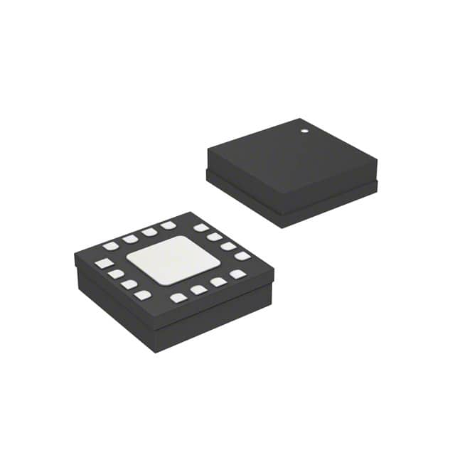
- Part No.:
- MP6507GQ-P
- Manufacturer:
- Monolithic Power Systems Inc.
- Category:
- Motor Drivers, Controllers
- Package:
- 16-VFQFN Exposed Pad
- Datasheet:
-
 MP6507GQ-P.pdf
- Description:
- IC MTR DRVR BIPOLR 2.7-15V 16QFN
- Quantity:
- Payment:

- Shipping:

Inventory:4,818
Please send an inquiry. Send us your inquiry, and we will respond immediately.
Product details
Overview
MP6507GQ-P from Monolithic Power Systems is a bipolar stepper-motor driver IC with dual integrated N-channel full-bridge MOSFETs, operating from 2.7V to 15V and delivering up to 700mA per channel. It features internal charge pump, 1.1mA quiescent current, thermal shutdown with fault flag output, and supports both external PWM and internal constant-off-time current control for precise winding current regulation in POS printers and security cameras.
For engineers reviewing the MP6507GQ-P datasheet, MP6507GQ-P pinout, MP6507GQ-P application, or MP6507GQ-P equivalent, key selection criteria include its 3×3mm QFN package with exposed thermal pad, dual full-bridge topology, 185mV current-sense threshold, 27µs constant off-time, and sleep-mode leakage of 1µA - all critical for battery-powered motion control designs requiring low power and thermal robustness.
Technical Context
The MP6507GQ-P implements two independent full-bridge drivers using eight N-channel MOSFETs with matched on-resistance (HS/LS ≈ 460mΩ/395mΩ at 5V, 25°C). Its internal charge pump enables high-side gate drive without external components, while the constant-off-time PWM current controller uses an external sense resistor and 185mV trip threshold to regulate motor current with 2.7µs blanking time to suppress switching noise.
Control logic accepts standard TTL/CMOS inputs (AIN1/AIN2/BIN1/BIN2) to configure full-step, half-step, or microstepping via external sequencing; nSLEEP enables 1µA standby mode with ~1.5ms wake-up delay. Fault reporting is provided via open-drain FAULT pin asserting low during over-temperature (165°C trigger, 15°C hysteresis) or UVLO conditions.
Key Specifications
| Parameter | Value and Actual Design Meaning |
|---|---|
| Supply Voltage Range | 2.7V to 15V - supports single-cell Li-ion to multi-cell alkaline/battery packs and 12V industrial rails. |
| Output Current per Channel | 700mA continuous - sufficient for NEMA 8–11 stepper motors in compact optical and portable equipment. |
| High-Side RDS(on) | 460mΩ (typ, 5V, 25°C) - limits conduction loss to <160mW per bridge at 700mA, enabling thermally constrained PCB layouts. |
| Current Sense Threshold | 185mV (typ) - sets motor current limit as ILIMIT = 0.185V / RSENSE, allowing precise 100–700mA tuning with standard 0.1–2Ω resistors. |
| Constant Off-Time | 27µs (typ) - determines maximum chopper frequency (~37kHz) and governs current ripple magnitude in internal PWM mode. |
| Sleep Current | 1µA (typ, VIN=5V) - extends battery life in always-on devices like security camera pan-tilt mechanisms between motion events. |
| Thermal Shutdown | 165°C junction temperature - protects against sustained overload or poor heatsinking; recovers at ~150°C. |
Pinout & Package
MP6507GQ-P is housed in a thermally enhanced 3mm × 3mm QFN-16 package with exposed thermal pad (connected to GND), optimized for compact motor-control PCBs requiring efficient heat dissipation without heatsinks.
| Pin/Terminal | Circuit Role | Design Meaning |
|---|---|---|
| 1 (SENA) | Channel A current sense input | Connects to low-side sense resistor (RSENA) for internal current regulation; referenced to GND. |
| 2 (AOUT2) | Motor winding A output (low-side) | Drives one end of phase-A winding; complements AOUT1 in full-bridge configuration. |
| 3 (BOUT2) | Motor winding B output (low-side) | Drives one end of phase-B winding; complements BOUT1 in full-bridge configuration. |
| 4 (SENB) | Channel B current sense input | Connects to low-side sense resistor (RSENB) for independent phase-B current control. |
| 5 (BOUT1) | Motor winding B output (high-side) | Drives opposite end of phase-B winding; driven by internal high-side MOSFET with charge pump. |
| 6 (FAULT) | Open-drain fault indicator | Pulls low during thermal shutdown or UVLO; requires external pull-up for system-level fault detection. |
| 7 (BIN1) | Phase B high-side gate control | Digital input controlling BOUT1; logic high enables high-side MOSFET when paired with appropriate BIN2 state. |
| 8 (BIN2) | Phase B low-side gate control | Digital input controlling BOUT2; used with BIN1 to set bridge state (H-H, H-L, L-H, L-L). |
| 9 (BST) | Charge pump output | Connects to 10nF–100nF ceramic capacitor to VIN to generate boosted gate voltage for high-side N-MOSFETs. |
| 10 (VIN) | Main power supply input | Accepts 2.7–15V; powers internal regulators, gate drivers, and MOSFET bridges; requires local 10µF bulk capacitance. |
| 11 (GND) | Power and signal ground | Common reference for all analog/digital circuits; must be tied directly to exposed thermal pad for thermal and EMI performance. |
| 12 (VDD) | Internal logic supply | Internally regulated ~5V rail; requires 2.2µF ceramic capacitor to GND; no external loading permitted. |
| 13 (AIN2) | Phase A low-side gate control | Digital input controlling AOUT2; used with AIN1 to define phase-A bridge output polarity and decay mode. |
| 14 (AIN1) | Phase A high-side gate control | Digital input controlling AOUT1; determines forward/reverse direction and step sequence timing in external PWM mode. |
| 15 (nSLEEP) | Active-low sleep enable | Pulling low disables all bridges and shuts down charge pump/regulator, reducing supply current to 1µA. |
| 16 (AOUT1) | Motor winding A output (high-side) | Drives opposite end of phase-A winding; driven by internal high-side MOSFET with charge pump. |
Key Features
| Feature | Design Value |
|---|---|
| Dual full-bridge topology with integrated N-MOSFETs | Eliminates need for 8 discrete power switches and associated gate drivers, reducing BOM count and layout area by >50% versus discrete solutions. |
| Internal charge pump for high-side drive | Enables full N-MOSFET bridges without external bootstrap capacitors or P-MOSFET compromises, improving efficiency and simplifying layout. |
| Programmable current regulation via external sense resistors | Allows precise motor current setting from 100mA to 700mA using standard 0.1–2Ω SMD resistors, supporting diverse torque and thermal requirements. |
| 1µA sleep-mode current | Extends operational battery life in portable devices (e.g., handheld scanners) by minimizing quiescent drain during idle periods. |
| Over-temperature fault flag with hysteresis | Provides reliable thermal protection with 15°C hysteresis (165°C trip → 150°C recovery), preventing repeated cycling under marginal cooling conditions. |
Applications
| POS Printers | Video Security Cameras |
|---|---|
Use Scenario: Bidirectional paper feed and print-head positioning in compact thermal receipt printers. IC Role / Device Role / Timing Role: Dual full-bridge driver executing half-step sequences to achieve 1.8° step resolution with smooth microstepping-compatible timing. Use Value: 700mA per channel delivers sufficient torque for rapid paper advancement while 1.1mA quiescent current minimizes standby power in always-connected retail terminals. | Use Scenario: Pan-and-tilt motion control in IP-based dome cameras with silent, jitter-free positioning. IC Role / Device Role / Timing Role: Bipolar stepper driver managing synchronized A/B winding excitation to execute precise angular movements under MCU command. Use Value: Internal PWM current control ensures consistent torque across varying supply voltages (5–12V), eliminating position drift during battery backup operation. |
| Digital Still Cameras | Battery-Powered Toys |
Use Scenario: Autofocus lens actuation and optical image stabilization (OIS) correction in mirrorless camera modules. IC Role / Device Role / Timing Role: Low-noise stepper driver delivering sub-millisecond step response and precise current-controlled microsteps for vibration-sensitive optics. Use Value: 27µs constant off-time enables high-frequency chopper operation (>30kHz), suppressing audible motor whine while maintaining 700mA peak current for fast focus lock. | Use Scenario: Steering and articulation control in RC vehicles and robotic toys powered by 2–3 AA/AAA cells. IC Role / Device Role / Timing Role: Compact motor driver enabling dual-DC-motor or unipolar/bipolar stepper operation from limited 3–4.5V battery sources. Use Value: 2.7V minimum operating voltage allows full functionality down to near-dead battery levels, extending playtime without premature shutdown. |
Equivalent & Alternatives
The following parts are listed as comparable options for similar bipolar stepper-motor driver applications.
| Alternative Part | Technical Difference | Application Difference | Selection Advice |
|---|---|---|---|
| TB6600HG | Higher voltage (45V max), higher current (3.5A), larger HTSSOP28 package; no integrated charge pump - requires external bootstrap circuitry. | Targeted at industrial CNC and larger NEMA 17+ motors; unsuitable for space-constrained 3×3mm designs. | Select when driving high-torque motors beyond 700mA or requiring >15V operation; avoid for battery-powered portables due to size and complexity. |
| DRV8834 | Lower voltage (10.8V max), lower current (1.5A), 3×3mm QFN package; includes indexer and microstepping logic not present in MP6507GQ-P. | Designed for simplified MCU interface with built-in step/direction inputs; lacks direct gate control for custom PWM schemes. | Choose when system-level simplicity (step/dir interface) outweighs need for external PWM flexibility or extended 15V operation. |
Compared with TB6600HG and DRV8834, MP6507GQ-P uniquely balances 15V operation, 700mA capability, and 3×3mm footprint with direct gate control - making it optimal for compact, battery-aware stepper systems where thermal efficiency and layout simplicity are prioritized over integrated indexing or ultra-high current.
Availability
MP6507GQ-P is available at Aetrix Electronics and suitable for POS printers, video security cameras, digital still cameras, and battery-powered toys requiring stable component supply, thermal resilience, and compact motor-drive integration.
Supply support for MP6507GQ-P includes scheduled delivery planning, volume procurement assistance, BOM continuity management, traceable sourcing, and lifecycle availability coordination for OEM customers, industrial embedded developers, connected-device designers, and electronics production programs.
Manufacturer
Monolithic Power Systems (MPS) is a fabless semiconductor company specializing in high-performance analog and power ICs, with design centers across Asia and North America and global manufacturing partnerships.
The MP6507 product line targets cost-sensitive, space-constrained motion-control applications in consumer electronics and industrial peripherals, emphasizing integrated power stages, low quiescent power, and robust thermal protection without external support components.
FAQ
What is the recommended PCB layout practice for thermal management of MP6507GQ-P?
The exposed thermal pad on the MP6507GQ-P's QFN package must be soldered directly to a large copper pour tied to GND, with ≥6 thermal vias (0.3mm diameter, spaced ≤1mm apart) connecting to inner or bottom-layer ground planes. Keep sense resistors within 2mm of SENA/SENB pins and route high-current motor traces wide (≥0.5mm) and short to minimize IR drop and EMI.
Can MP6507GQ-P drive two independent DC motors instead of a stepper motor?
Yes - the dual full-bridge architecture allows independent control of two brushed DC motors. Apply complementary PWM signals to AIN1/AIN2 for motor A and BIN1/BIN2 for motor B. Each bridge supports bidirectional rotation and braking; current limiting remains active per channel via separate SENA/SENB sense paths.
How does the internal blanking time affect current regulation accuracy?
The 2.7µs blanking time prevents false current-limit triggering during MOSFET switching transitions by disabling the sense comparator output. This ensures accurate current measurement only during stable conduction, but requires careful selection of RSENSE to maintain sufficient voltage margin above 185mV after blanking ends - especially at low currents or high PWM frequencies.
What external components are mandatory for basic MP6507GQ-P operation?
Mandatory components include: (1) 10µF input capacitor (VIN to GND), (2) 2.2µF VDD bypass capacitor (VDD to GND), (3) 10nF–100nF BST-to-VIN capacitor, (4) two current-sense resistors (RSENA/RSENB) sized per desired ILIMIT, and (5) pull-up on FAULT if monitoring is required. No bootstrap diodes or external regulators are needed.
Does MP6507GQ-P support microstepping, and if so, how is it implemented?
MP6507GQ-P does not include native microstepping logic but supports waveform-based microstepping via external MCU control of AIN1/AIN2/BIN1/BIN2. By applying precise PWM duty cycles and phase offsets to the four gate inputs, fractional step positions (e.g., 1/4, 1/8, 1/16) can be achieved - though current regulation remains at full/half-step granularity unless combined with external DAC-based current profiling.
What is the maximum allowable motor supply voltage when using MP6507GQ-P?
The absolute maximum VIN rating is 18V, but the recommended operating range is 2.7V to 15V per datasheet specifications. Exceeding 15V risks violating safe operating area limits under load, particularly at elevated temperatures; sustained operation above 15V voids guaranteed performance and may trigger UVLO or thermal shutdown unpredictably.
How does the FAULT pin behave during UVLO versus thermal shutdown?
The FAULT pin asserts low for both conditions - UVLO (VIN < 2.5V rising threshold) and thermal shutdown (TJ > 165°C). It remains low until the fault condition clears: UVLO recovers when VIN exceeds 2.57V (2.5V + 70mV hysteresis); thermal recovery occurs at ~150°C. No distinction between fault types is provided on this pin; external monitoring requires correlating with VIN and temperature sensors.
MP6507GQ-P Specifications
- Product attributes
- Attribute value
- Manufacturer:
- Monolithic Power Systems Inc.
- Series:
- -
- Package/Case:
- 16-VFQFN Exposed Pad
- Packaging:
- Tape & Reel (TR)
- Product Status:
- Active
- Motor Type - Stepper:
- Bipolar
- Motor Type - AC, DC:
- Brushed DC
- Function:
- Driver - Fully Integrated, Control and Power Stage
- Output Configuration:
- Half Bridge (4)
- Interface:
- Parallel
- Technology:
- Power MOSFET
- Step Resolution:
- 1, 1/2
- Applications:
- Battery Powered
- Current - Output:
- 700mA
- Voltage - Supply:
- 2.7V ~ 15V
- Voltage - Load:
- -
- Operating Temperature:
- -40°C ~ 125°C (TJ)
- Grade:
- -
- Qualification:
- -
- Mounting Type:
- Surface Mount
- Supplier Device Package:
- 16-QFN (3x3)
MP6507GQ-P FAQ
1.How can I place an order for MP6507GQ-P through Aetrix?
Please submit a Request for Quotation (RFQ) for MP6507GQ-P on Aetrix. Our sales agent will provide a competitive quotation and guide you through the order confirmation once you accept the terms.
2.Are the price and stock information for MP6507GQ-P reliable?
The price and inventory of MP6507GQ-P are updated periodically and may fluctuate due to market conditions. Stock and pricing data are typically refreshed every 24 hours. Quotation validity for MP6507GQ-P is usually 5 days.
3.What payment methods are accepted for MP6507GQ-P?
We accept Wire Transfer, PayPal, Credit Card, Western Union, MoneyGram, and Escrow for MP6507GQ-P transactions.
Note: Certain payment methods may incur a processing fee.
4.How is shipping managed for MP6507GQ-P?
MP6507GQ-P orders can be shipped via leading logistics carriers, including DHL, UPS, FedEx, TNT, or Registered Mail.
Once your MP6507GQ-P order is processed, you will receive an email with the shipment details and tracking number.
Note: Tracking information may take up to 24 hours to appear. Express delivery typically takes 3–5 business days.
5.How can I obtain technical support or documentation for MP6507GQ-P?
For technical support, including MP6507GQ-P datasheets, pinout diagrams, or application guidance, please contact our engineering support team. They can provide detailed documentation and assistance for your MP6507GQ-P requirements.
6.How does Aetrix verify that MP6507GQ-P is sourced from the original manufacturer or authorized distributors?
All MP6507GQ-P products on Aetrix are procured from qualified distributors and authorized channels. Our dedicated quality assurance team conducts strict verification, including traceability checks and, if necessary, third-party testing. This ensures that MP6507GQ-P meets industry standards.
7.What is the process for return or replacement of MP6507GQ-P?
All MP6507GQ-P units undergo pre-shipment inspection (PSI). If there is an issue with MP6507GQ-P, returns or replacements are accepted under the following conditions:
1.Quantity discrepancies, incorrect items, or visible external defects (such as breakage or corrosion), acknowledged by Aetrix.
2.The issue is reported within 90 days of delivery.
3.The MP6507GQ-P part is unused and in its original packaging.
Return procedure for MP6507GQ-P:
1.Submit a request within 90 days.
2.Obtain a Return Material Authorization (RMA) from Aetrix.
MP6507GQ-P Tags

-
DRV2603RUNR
Texas Instruments

-
DRV8837CDSGR
Texas Instruments

-
DRV8837DSGR
Texas Instruments
-
DRV8838DSGR
Texas Instruments

-
DRV8839DSSR
Texas Instruments

-
EMC2301-1-ACZL-TR
Microchip Technology
-
DRV8231ADSGR
Texas Instruments

-
EMC2302-2-AIZL-TR
Microchip Technology

-
DRV8800PWPR
Texas Instruments
-
DRV8835DSSR
Texas Instruments

-
EMC2303-1-KP-TR
Microchip Technology

-
DRV8876PWPR
Texas Instruments
Tech Hub

A practical engineering guide to 3.3V and 5V logic compatibility, input thresholds, resistor dividers, translator ICs, MOSFET level shifting, I2C pull-ups, timing limits and power-sequencing risks.

The 74HC595 uses push-pull logic outputs, while the TPIC6B595 uses 50 V open-drain DMOS sinks for higher-power loads. This guide compares timing, current limits, 3.3 V interfacing, load wiring, thermal…

The 74HC595 converts serial data into eight stable parallel outputs. This guide covers pin functions, shift and storage timing, OE and MR behavior, drive-current limits, cascading, voltage compatibilit…

A technical comparison of level-sensitive latches and edge-triggered flip-flops, covering timing windows, setup and hold limits, master–slave operation, time borrowing, race-through, HDL inference and…

A D latch stores one bit while Enable controls when data can pass. This reference covers gate-level operation, truth tables, transparency, setup and hold timing, LE versus OE, common ICs and practical …

An SR latch stores one bit through cross-coupled feedback. This engineering reference covers NOR and NAND implementations, truth tables, forbidden-state recovery, gated operation, switch debouncing, fa…

Latch circuits retain one bit through feedback. This technical reference covers SR and D latches, truth tables, transparency, timing limits, latch-versus-flip-flop behavior, applications and common log…

An engineering guide to LED driver operation, constant-current and constant-voltage outputs, linear and switching topologies, dimming, IC selection, calculations, replacement compatibility, and fault c…

Operational amplifier guide covering op amp basics, feedback, ideal vs real op amps, common configurations, buffer circuits, offset, bias current, gain-bandwidth, slew rate, rail-to-rail limits and sel…

Jumper cables guide covering safe connection order, red and black clamp placement, final ground connection, cable gauge, length, clamp quality, copper vs CCA cables, jump starter comparison and battery…


