
 My Inquiry
 My Account


Monolithic Power Systems Inc. MP6972GS-Z
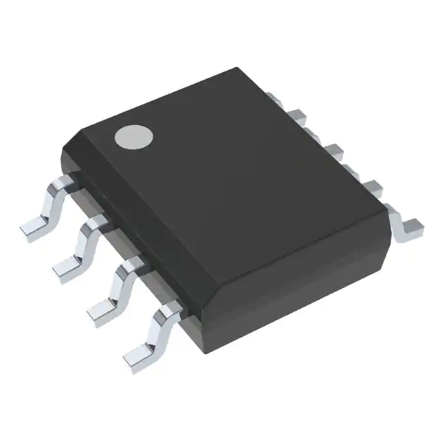
- Part No.:
- MP6972GS-Z
- Manufacturer:
- Monolithic Power Systems Inc.
- Category:
- OR Controllers, Ideal Diodes
- Package:
- 8-SOIC (0.154", 3.90mm Width)
- Datasheet:
-
 MP6972GS-Z.pdf
- Description:
- CCM/DCM FLYBACK IDEAL DIODE WITH
- Quantity:
- Payment:

- Shipping:

Inventory:2,485
Please send an inquiry. Send us your inquiry, and we will respond immediately.
Product details
Overview
MP6972GS-Z from Monolithic Power Systems is a CCM/DCM flyback synchronous rectifier IC integrating a 100V/17mΩ MOSFET for low-side secondary-side rectification. It regulates forward voltage drop to 40mV, achieves 25ns turn-off delay, employs slew-rate detection to prevent false turn-on during DCM/QR ringing, and operates across -40°C to +125°C junction temperature with 110µA quiescent current - deployed in USB PD and QC laptop adapters.
For engineers reviewing the MP6972GS-Z datasheet, MP6972GS-Z pinout, MP6972GS-Z application, or MP6972GS-Z equivalent, key selection criteria include its integrated 100V MOSFET RDS(ON), VFWD regulation accuracy, DCM/CCM/QR mode compatibility, SOIC-8 thermal performance (θJA = 67°C/W), and VDD generation architecture using SENSE/HVC dual-input regulation.
Technical Context
The MP6972GS-Z implements intelligent gate control via real-time VDS sensing: it initiates turn-on only when dVDS/dt exceeds 30ns slew threshold and VDS crosses -80mV, then enforces 1.2µs blanking to suppress ringing-induced misfires. Its VDD regulator dynamically selects between SENSE (5V) and HVC (6.7V) inputs based on voltage level and internal diode drop.
During conduction, the IC actively modulates gate drive to clamp VSD at ~40mV across load current, minimizing conduction loss while maintaining fast turn-off (25ns delay) before reverse recovery. Turn-off is triggered at -3mV VDS, followed by 2V blanking threshold release to avoid premature reactivation.
Key Specifications
| Parameter | Value and Actual Design Meaning |
|---|---|
| VDS Breakdown | 100V - supports universal input flyback designs up to 265VAC primary with margin |
| RDS(ON) | 17mΩ @ VGS = 6.7V - enables <2.5A continuous output in typical 30W adapters without external heatsink |
| VFWD Regulation | 40mV - maintains consistent low forward drop across wide load range, reducing I²R loss vs. diodes |
| Turn-off Delay | 25ns - ensures sub-100ns total turn-off time critical for CCM operation to prevent shoot-through |
| Quiescent Current | 110µA - minimizes no-load power loss, supporting Energy Star Tier 2 standby compliance |
| Operating Temp | -40°C to +125°C - qualified for industrial-grade adapter environments with full parameter guarantee |
| VDD UVLO | 4.2V rising / 4.0V falling - provides clean startup and brown-out protection in variable-output systems |
Pinout & Package
MP6972GS-Z is housed in an SOIC-8 package with exposed thermal pad (JEDEC MS-012 AA), offering 67°C/W junction-to-ambient thermal resistance on standard 4-layer PCBs. Pin 1 is located at the top-left corner adjacent to the notch or dot marking.
| Pin/Terminal | Circuit Role | Design Meaning |
|---|---|---|
| 1, 4 VS | MOSFET source reference | Common source node for internal FET and VDD regulator ground reference; connects directly to output return |
| 2 HVC | High-voltage linear regulator input | Accepts up to 180V for auxiliary VDD charging; enables self-powered operation without auxiliary winding |
| 3 SENSE | Drain voltage sensing input | Detects VDS for turn-on/turn-off decisions; requires low-inductance routing to drain node |
| 5 VDD | Internal LDO output | 5V/6.7V regulated supply for control circuitry; decoupled with local 1µF ceramic capacitor |
| 6, 7, 8 VD | MOSFET drain terminals | Parallel-connected high-current drain paths; must be routed with wide copper to minimize RDS(ON) rise and thermal impedance |
Key Features
| Feature | Design Value |
|---|---|
| Slew-rate–based turn-on detection | Rejects DCM/QR ringing false triggers by requiring dVDS/dt > threshold within 30ns window |
| Adaptive VFWD regulation | Maintains 40mV forward drop across 0–2.5A output, eliminating diode VF variation losses |
| Dual-input VDD generation | Automatically switches between SENSE (5V) and HVC (6.7V) sources for robust startup and wide-input operation |
| Programmable turn-off timing | SENSE pin placement distance from VD adjusts effective turn-off point for CCM optimization |
| Integrated 100V MOSFET | Eliminates external FET, gate driver, and sense resistor - reduces BOM count and layout complexity |
Applications
| Laptop AC Adapters | USB PD Fast Chargers |
|---|---|
Use Scenario: 45W–65W universal-input flyback converter powering 15–20V laptop systems with 2.5A output. IC Role / Device Role / Timing Role: Low-side synchronous rectifier replacing Schottky diode; controls MOSFET gate to regulate VSD and enforce zero-current turn-off. Use Value: Enables >94% efficiency at full load and <75mW no-load consumption, meeting DOE Level VI and Energy Star requirements. | Use Scenario: Multi-port USB PD 3.0 charger delivering 20V/3A with adaptive voltage scaling and dynamic load sharing. IC Role / Device Role / Timing Role: Secondary-side intelligent rectifier operating in CCM/DCM/QR modes; synchronizes with primary controller via VDS sensing. Use Value: Reduces secondary-side conduction loss by 65% vs. 40V Schottky, enabling smaller magnetics and higher power density in compact form factors. |
| QC 3.0 Wall Adapters | Industrial Flyback Power Supplies |
Use Scenario: 18W–36W quick-charge wall adapter supporting 9V/2A and 12V/1.5A profiles with tight output regulation. IC Role / Device Role / Timing Role: Fast-turn-off SR controller with 25ns delay and 1.2µs blanking; manages transitions across variable output voltages. Use Value: Achieves <100mV output ripple under transient load steps and eliminates reverse-recovery spikes that degrade EMI filter design. | Use Scenario: 24V/1A isolated flyback supplying PLC I/O modules in factory automation with extended temperature operation. IC Role / Device Role / Timing Role: High-reliability synchronous rectifier rated for -40°C to +125°C; uses HVC input for auxiliary-free startup in unregulated bus applications. Use Value: Delivers 2.1W max power dissipation margin at 100°C ambient, enabling convection-cooled designs without derating. |
Equivalent & Alternatives
The following parts are listed as comparable options for similar flyback synchronous rectifier applications.
| Alternative Part | Technical Difference | Application Difference | Selection Advice |
|---|---|---|---|
| MP6971GS-Z | Lower 60V VDS rating; identical 40mV VFWD regulation and SOIC-8 package | Restricted to ≤12V output designs; unsuitable for 20V USB PD or QC 3.0 | Select when output voltage ≤12V and cost sensitivity outweighs voltage margin needs |
| ONSEMI NCP4307DR2G | External MOSFET required; 100V rating but no integrated FET; 35mV VFWD target | Higher BOM count and layout complexity; better thermal scalability for >3A outputs | Select when discrete FET selection (e.g., 5mΩ SiC) or thermal customization is prioritized over integration |
Compared with MP6971GS-Z, MP6972GS-Z delivers 67% higher voltage headroom for 20V USB PD; versus NCP4307DR2G, it reduces component count by 4 parts and simplifies layout but trades off thermal flexibility for integration.
Availability
MP6972GS-Z is available at Aetrix Electronics and suitable for laptop adapters, USB PD fast chargers, and industrial flyback converters requiring stable component supply, RoHS-compliant packaging, and long-term lifecycle support.
Supply support for MP6972GS-Z includes scheduled delivery planning, volume procurement assistance, BOM continuity management, traceable sourcing, and lifecycle availability coordination for OEM customers, industrial embedded developers, connected-device designers, and electronics production programs.
Manufacturer
Monolithic Power Systems (MPS) is a fabless semiconductor company specializing in high-performance power management ICs, with design centers in the US, China, and Taiwan, and global manufacturing partnerships.
The MP697x series targets high-efficiency AC/DC secondary-side rectification, specifically engineered to replace Schottky diodes in flyback topologies while supporting CCM, DCM, and QR operation without external timing components.
FAQ
What is the maximum continuous output current supported by MP6972GS-Z?
The MP6972GS-Z is rated for 2.5A continuous output in typical universal-input 30W adapters, validated per thermal modeling using θJA = 67°C/W and 150°C max junction temperature. At 100°C ambient, power loss budget allows ~1.2W total dissipation, limiting practical current to 2.5A with standard PCB copper area and no heatsink.
How does the slew-rate detection prevent false turn-on during DCM ringing?
Slew-rate detection requires VDS to fall faster than 30ns to trigger turn-on; DCM ringing exhibits slow dVDS/dt (<10ns/µs), so even if VDS dips below -80mV, the IC ignores it. Only primary-side turn-off events produce fast edges (>1V/ns), ensuring reliable activation only during true conduction periods.
Can MP6972GS-Z operate without an auxiliary winding?
Yes - the HVC pin accepts up to 180V, allowing direct connection to the transformer secondary or rectified output to power the IC. This eliminates need for auxiliary winding in low-side configurations, simplifying transformer design and reducing leakage inductance concerns.
What is the purpose of the external resistor between SENSE and VD?
A 100–300Ω resistor limits peak current into the SENSE pin during body-diode conduction events, preventing violation of the -1V absolute minimum rating. It also dampens high-frequency ringing without degrading VDS edge detection speed, as confirmed by slew-rate analysis in the datasheet's Application Information section.
How does VDD regulation switch between SENSE and HVC inputs?
VDD regulation uses internal comparators: below 5.7V, VDD is clamped at 5V (VDD_SENSE); between 5.7V and 6.7V, VDD tracks HVC minus 0.7V (diode drop); above 6.7V, VDD is regulated at 6.7V (VDD_HVC). This ensures stable bias across wide input/output conditions without external regulators.
Is MP6972GS-Z compatible with quasi-resonant (QR) controllers?
Yes - the MP6972GS-Z explicitly supports QR operation via its ringing detection circuitry and 1.2µs turn-on blanking time, which prevents false triggering during resonant valley switching. Timing diagrams and test waveforms in the datasheet confirm stable operation with common QR controllers like MP6901 and UCC28740.
What thermal enhancements improve MP6972GS-Z's power handling in SOIC-8?
Thermal performance is enhanced by connecting pins 6–8 (VD) and pins 1–4 (VS) to large copper pours with multiple thermal vias to inner layers. The SOIC-8 package's exposed pad (though not soldered in standard variant) is designed for optional thermal pad attachment, reducing θJA by up to 15°C/W with proper PCB layout.
MP6972GS-Z Specifications
- Product attributes
- Attribute value
- Manufacturer:
- Monolithic Power Systems Inc.
- Series:
- -
- Package/Case:
- 8-SOIC (0.154", 3.90mm Width)
- Packaging:
- Tape & Reel (TR)
- Product Status:
- Active
- Type:
- Flyback
- FET Type:
- N-Channel
- Ratio - Input:Output:
- 1:1
- Internal Switch(s):
- Yes
- Delay Time - ON:
- 20 ns
- Delay Time - OFF:
- 25 ns
- Current - Output (Max):
- -
- Current - Supply:
- 2.4 mA
- Voltage - Supply:
- 4.5V ~ 13V
- Applications:
- General Purpose
- Operating Temperature:
- -40°C ~ 125°C (TJ)
- Grade:
- -
- Qualification:
- -
- Mounting Type:
- Surface Mount
- Supplier Device Package:
- 8-SOIC
MP6972GS-Z FAQ
1.How can I place an order for MP6972GS-Z through Aetrix?
Please submit a Request for Quotation (RFQ) for MP6972GS-Z on Aetrix. Our sales agent will provide a competitive quotation and guide you through the order confirmation once you accept the terms.
2.Are the price and stock information for MP6972GS-Z reliable?
The price and inventory of MP6972GS-Z are updated periodically and may fluctuate due to market conditions. Stock and pricing data are typically refreshed every 24 hours. Quotation validity for MP6972GS-Z is usually 5 days.
3.What payment methods are accepted for MP6972GS-Z?
We accept Wire Transfer, PayPal, Credit Card, Western Union, MoneyGram, and Escrow for MP6972GS-Z transactions.
Note: Certain payment methods may incur a processing fee.
4.How is shipping managed for MP6972GS-Z?
MP6972GS-Z orders can be shipped via leading logistics carriers, including DHL, UPS, FedEx, TNT, or Registered Mail.
Once your MP6972GS-Z order is processed, you will receive an email with the shipment details and tracking number.
Note: Tracking information may take up to 24 hours to appear. Express delivery typically takes 3–5 business days.
5.How can I obtain technical support or documentation for MP6972GS-Z?
For technical support, including MP6972GS-Z datasheets, pinout diagrams, or application guidance, please contact our engineering support team. They can provide detailed documentation and assistance for your MP6972GS-Z requirements.
6.How does Aetrix verify that MP6972GS-Z is sourced from the original manufacturer or authorized distributors?
All MP6972GS-Z products on Aetrix are procured from qualified distributors and authorized channels. Our dedicated quality assurance team conducts strict verification, including traceability checks and, if necessary, third-party testing. This ensures that MP6972GS-Z meets industry standards.
7.What is the process for return or replacement of MP6972GS-Z?
All MP6972GS-Z units undergo pre-shipment inspection (PSI). If there is an issue with MP6972GS-Z, returns or replacements are accepted under the following conditions:
1.Quantity discrepancies, incorrect items, or visible external defects (such as breakage or corrosion), acknowledged by Aetrix.
2.The issue is reported within 90 days of delivery.
3.The MP6972GS-Z part is unused and in its original packaging.
Return procedure for MP6972GS-Z:
1.Submit a request within 90 days.
2.Obtain a Return Material Authorization (RMA) from Aetrix.
MP6972GS-Z Tags

-
LM66100DCKR
Texas Instruments
-
LM66200DRLR
Texas Instruments
-
LM66100DCKT
Texas Instruments

-
AP74700QW6-7
Diodes Incorporated
-
LM73100RPWR
Texas Instruments
-
LM74502DDFR
Texas Instruments
-
LM74700QDBVRQ1
Texas Instruments
-
MAX40200AUK+T
Analog Devices Inc./Maxim Integrated
-
MAX40200ANS+T
Analog Devices Inc./Maxim Integrated
-
MAX40203AUK+T
Analog Devices Inc./Maxim Integrated
-
MAX40203ANS+T
Analog Devices Inc./Maxim Integrated
-
LM74502QDDFRQ1
Texas Instruments
Tech Hub

Operational amplifier guide covering op amp basics, feedback, ideal vs real op amps, common configurations, buffer circuits, offset, bias current, gain-bandwidth, slew rate, rail-to-rail limits and sel…

Jumper cables guide covering safe connection order, red and black clamp placement, final ground connection, cable gauge, length, clamp quality, copper vs CCA cables, jump starter comparison and battery…

LDO regulator guide covering low dropout voltage, power dissipation, thermal design, PSRR, output noise, capacitor stability, adjustable LDO circuits, LDO vs buck converter and datasheet selection chec…

Conditional Access Module guide covering CAM meaning, CI/CI+ interface, smart card authorization, DVB security workflow, TV and set-top box compatibility, internal electronics, ESD protection, connecto…

Guide to electronic component obsolescence covering EOL risk, PCN/PDN notices, last-time buy planning, replacement options, form-fit-function validation, counterfeit risk and BOM lifecycle management.

18650 battery guide covering lithium-ion cell basics, 3.6V/3.7V voltage, 4.2V charging, mAh and Wh capacity, protected cells, chargers, BMS, series-parallel packs, holders, welding and sourcing checks.…

Hall effect sensor guide covering working principle, linear and digital sensors, Arduino circuits, current sensing, speed detection, automotive applications, A3144 examples, signal filtering and datash…

Product Change Notification guide for electronic components, covering PCN meaning, PCN vs PDN/EOL, common change types, risk levels, form-fit-function review, engineering validation, BOM control, LTB/L…

A practical guide to blend door actuators, covering HVAC function, symptoms, location, AC and heater issues, reset and calibration, replacement cost, electrical diagnosis, compatibility checks, and rep…

Engineering guide to Raspberry Pi alternatives, covering chip-level differences, Orange Pi, ROCK, Jetson, Banana Pi, NanoPi, Compute Module, Pico, GPIO, camera, HAT compatibility, and replacement risks…


