
 My Inquiry
 My Account


NXP Semiconductors MPC5565MVZ132
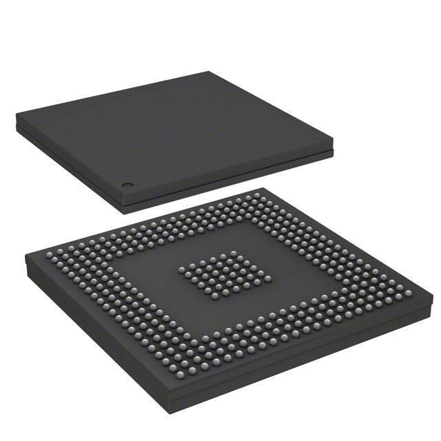
- Part No.:
- MPC5565MVZ132
- Manufacturer:
- NXP Semiconductors
- Category:
- Microcontrollers
- Package:
- 324-BBGA
- Datasheet:
-
 MPC5565MVZ132.pdf
- Description:
- IC MCU 32BIT 2MB FLASH 324PBGA
- Quantity:
- Payment:

- Shipping:

Inventory:3,856
Please send an inquiry. Send us your inquiry, and we will respond immediately.
Product details
Overview
MPC5565MVZ132 from Freescale Semiconductor is a Power Architecture®-based 32-bit automotive-grade microcontroller with a 132 MHz nominal system clock (135 MHz max), 2 MB on-chip flash, 80 KB SRAM, and integrated eTPU/eMIOS timer subsystems. It features dual FlexCAN interfaces, four DSPI modules, two eSCI ports, and a 40-channel eQADC - deployed in engine control units, transmission controllers, and chassis domain controllers requiring ASIL-B functional safety compliance.
For engineers reviewing the MPC5565MVZ132 datasheet, MPC5565MVZ132 pinout, MPC5565MVZ132 application, or MPC5565MVZ132 equivalent, key selection criteria include its 324-pin PBGA Pb-free package, –40°C to +125°C operating range, VLE instruction set for code density reduction, dual-core lockstep readiness (via external monitoring), and integrated voltage regulator controller (VRC) supporting external pass transistor regulation.
Technical Context
The MPC5565MVZ132 implements a PowerPC e200z6 core enhanced with Variable Length Encoding (VLE), enabling mixed 16-/32-bit instructions to reduce firmware footprint by up to 30% versus legacy PowerPC encoding. Its memory hierarchy includes 8 KB unified cache, 80 KB on-chip SRAM, and 2 MB flash with H7Fa architecture supporting single-cycle read access and 100k erase cycles.
Real-time peripheral control is handled by two independent engines: the 32-channel enhanced Time Processor Unit (eTPU) with 24-bit timers and angle-clock hardware for motor/sensor timing, and the 24-channel enhanced Modular I/O System (eMIOS) supporting edge- and center-aligned PWM for inverter gate drive. All serial interfaces - FlexCAN, DSPI, eSCI - operate independently of CPU load via DMA and queue-based buffering.
Key Specifications
| Parameter | Value and Actual Design Meaning |
|---|---|
| Core Architecture | PowerPC e200z6 with VLE extension - enables compact firmware image and deterministic interrupt latency under 100 ns. |
| Max System Clock | 132 MHz nominal / 135 MHz max with ±2% FM - supports real-time control loops at ≤7.5 µs cycle time. |
| Flash Memory | 2 MB H7Fa flash - provides dual-bank operation for safe over-the-air (OTA) updates without runtime interruption. |
| eQADC Channels | 40-channel 12-bit eQADC - delivers synchronized sampling across multiple sensors with hardware-triggered conversion sequences. |
| FlexCAN Interfaces | Dual CAN 2.0B controllers - each supports 64-message objects, programmable bit timing, and bus-off recovery without CPU intervention. |
| Operating Temperature | –40°C to +125°C ambient - qualified per AEC-Q100 Grade 1, enabling direct placement in powertrain compartments. |
| Supply Voltages | 1.5 V core (±10%), 3.3 V I/O (VDD33/VDDSYN), 5.0 V analog (VDDA/VDDEH) - supports mixed-voltage sensor interfacing and robust ESD immunity. |
Pinout & Package
The MPC5565MVZ132 is housed in a 324-ball plastic ball grid array (PBGA) package with 1.0 mm ball pitch, JEDEC MO-251 compliant, and lead-free (Pb-free) finish. Thermal resistance is 19°C/W (RθJA, 4-layer board) and 10°C/W (RθJB), enabling conduction-cooled designs without heatsinks up to 2.5 W dissipation.
| Pin/Terminal | Circuit Role | Design Meaning |
|---|---|---|
| VDD (Balls A1–A4, B1–B4, etc.) | 1.5 V Core Supply | Must be ramped to ≥1.35 V before VDDSYN to prevent PLL lock failure during power-up sequencing. |
| VDDSYN (Balls C1, C2, D1, D2) | 3.3 V Clock Synthesizer Supply | Powers FMPLL and SIU; requires ≤100 mV delta vs. VRC33 during power-up to avoid VRC pass-transistor current spikes. |
| VRC33 (Ball E1) | Voltage Regulator Controller Reference | Drives external NPN pass transistor; must be ≥2.0 V to fully enable 1.5 V regulation and sustain full-speed operation. |
| eTPU_A[0:31] (Balls G1–K12) | eTPU Channel I/O | Hardware-timed capture/compare signals with <10 ns jitter; supports resolver, encoder, and injector timing with angle-clock sync. |
| FLEXCAN0_TX/RX (Balls M1/M2) | Controller Area Network Interface | Direct CAN physical layer interface; supports ISO 11898-2 signaling and automatic retransmission on arbitration loss. |
| eQADC0[0:39] (Balls P1–T12) | Analog Input Multiplexer Inputs | 40 dedicated analog input pins with programmable gain (1×/2×/4×/8×) and hardware-triggered scan sequences. |
Key Features
| Feature | Design Value |
|---|---|
| VLE Instruction Set | Reduces compiled code size by ~25–30% versus standard PowerPC encoding, lowering flash cost and boot time in resource-constrained ECUs. |
| eTPU Engine | Offloads 32 high-precision timing channels from CPU - enables simultaneous camshaft position decoding, fuel injection timing, and knock detection. |
| H7Fa Flash Architecture | Supports background read while programming (BRWP), ECC protection, and dual-bank partitioning for fail-safe OTA updates. |
| SIU Pad Configuration | Runtime-configurable I/O pad types (fast/medium/slow), slew rate control, and weak pull-up/down - eliminates external biasing components. |
| Integrated VRC | Eliminates need for external voltage regulator IC; supports discrete NPN pass transistor with thermal foldback and current limiting. |
Applications
| Engine Control Unit (ECU) | Electric Power Steering (EPS) |
|---|---|
|
Use Scenario: Real-time combustion timing, air-fuel ratio control, and OBD-II diagnostics in gasoline/diesel powertrains. IC Role / Device Role / Timing Role: Primary compute engine executing control laws at 10 kHz, managing 40+ analog sensor inputs and 16+ PWM outputs via eMIOS. Use Value: eTPU handles crank/cam synchronization with <50 ns jitter, while dual FlexCAN interfaces isolate diagnostic and actuator networks. |
Use Scenario: Torque assist calculation, motor phase commutation, and fault monitoring in 12 V/48 V EPS systems. IC Role / Device Role / Timing Role: Safety-critical controller implementing ASIL-B torque path with lockstep-capable dual-core monitoring and redundant ADC sampling. Use Value: 40-channel eQADC enables simultaneous sampling of motor current, temperature, and position sensors with hardware-triggered sequence alignment. |
| Transmission Control Module (TCM) | Brake-by-Wire Actuator |
|
Use Scenario: Gear shift scheduling, clutch pressure modulation, and hydraulic valve control in 8-speed automatic transmissions. IC Role / Device Role / Timing Role: High-integrity timing controller using eTPU for solenoid driver timing and eMIOS for PWM-controlled pressure regulators. Use Value: Dual-action eMIOS channels generate precise center-aligned PWM with dead-time insertion, reducing MOSFET shoot-through risk. |
Use Scenario: Redundant brake pressure generation and closed-loop control in electro-hydraulic brake (EHB) systems. IC Role / Device Role / Timing Role: Functional safety controller with dual FlexCAN for cross-checking commands and eQADC for redundant pressure feedback. Use Value: On-chip VRC ensures stable 1.5 V core supply during battery transients, maintaining CPU operation during 12 V dips to 6 V. |
Equivalent & Alternatives
The following parts are listed as comparable options for similar automotive microcontroller applications.
| Alternative Part | Technical Difference | Application Difference | Selection Advice |
|---|---|---|---|
| S32K144HAT0MLHT | ARM Cortex-M4F core, 80 MHz max, 512 KB flash, no eTPU, AEC-Q100 Grade 1. | Lacks hardware-accelerated timing engines; relies on CPU for PWM/encoder tasks - increases software complexity and jitter. | Preferred for new low-cost body electronics where VLE/eTPU not required and ARM toolchain familiarity exists. |
| MPC5674FZQ132 | Same e200z7 core, 132 MHz, 2 MB flash, but 256-pin LQFP package and no VRC - requires external 1.5 V regulator. | Lower I/O count and no integrated voltage regulation limit use in space-constrained, high-thermal-density modules. | Used where PCB layout favors LQFP and external power management is already present; not drop-in compatible. |
Compared with MPC5565MVZ132, S32K144HAT0MLHT offers lower cost and ARM ecosystem support but lacks deterministic hardware timing; MPC5674FZQ132 retains Power Architecture compatibility but sacrifices package density and integrated power control - making MPC5565MVZ132 optimal for thermally constrained, high-precision powertrain modules requiring minimal external components.
Availability
MPC5565MVZ132 is available at Aetrix Electronics and suitable for engine control units, electric power steering systems, and transmission control modules requiring stable component supply across extended automotive production lifecycles.
Supply support for MPC5565MVZ132 includes scheduled delivery planning, volume procurement assistance, BOM continuity management, traceable sourcing, and lifecycle availability coordination for OEM customers, industrial embedded developers, connected-device designers, and electronics production programs.
Manufacturer
Freescale Semiconductor (now part of NXP Semiconductors since 2015) is a pioneer in automotive microcontrollers, delivering high-reliability Power Architecture and S32 platforms for safety-critical vehicle systems.
The MPC5565MVZ132 belongs to the MPC5500 family - engineered specifically for real-time powertrain and chassis control, emphasizing deterministic timing, functional safety readiness, and integration of analog/motor control peripherals.
FAQ
What is the maximum junction temperature specification for the MPC5565MVZ132?
The MPC5565MVZ132 has a maximum junction temperature (TJ) of 150°C, validated per AEC-Q100 stress testing. This rating enables operation in under-hood environments where ambient temperatures reach 125°C and power dissipation approaches 2.5 W. Thermal design must maintain RθJA ≤ 19°C/W on a 4-layer board to ensure reliable long-term performance at full speed.
Does the MPC5565MVZ132 support functional safety standards such as ISO 26262?
Yes, the MPC5565MVZ132 is designed to support ASIL-B compliance per ISO 26262. It includes lockstep-capable dual-core monitoring (via external logic), ECC-protected flash/SRAM, built-in self-test (BIST) for memory, and diagnostic coverage for clock, reset, and power domains - all documented in the MPC5565 Functional Safety Manual (Freescale Doc. AN4543).
Can the MPC5565MVZ132 operate without an external voltage regulator?
Yes - the MPC5565MVZ132 integrates a Voltage Regulator Controller (VRC) that drives an external NPN pass transistor to generate its 1.5 V core supply from a 3.3 V or 5 V source. When configured per Freescale's reference design (including 1 µF phase compensation and 20 µF bulk capacitance), the VRC eliminates need for a discrete 1.5 V regulator IC.
What is the purpose of the Variable Length Encoding (VLE) feature in the MPC5565MVZ132?
VLE allows the MPC5565MVZ132 to execute mixed 16-bit and 32-bit instructions, reducing typical firmware image size by 25–30% compared to standard PowerPC encoding. This lowers flash memory cost, shortens boot time, and improves cache hit rates - critical for memory-constrained automotive ECUs where code density directly impacts real-time determinism.
How many CAN interfaces does the MPC5565MVZ132 support, and what protocol versions are implemented?
The MPC5565MVZ132 integrates two independent FlexCAN modules compliant with CAN 2.0B (ISO 11898-1), supporting both standard (11-bit) and extended (29-bit) identifiers, programmable bit timing, and automatic bus-off recovery. Each module includes 64 message buffers with hardware acceptance filtering and priority-based transmission scheduling.
MPC5565MVZ132 Specifications
- Product attributes
- Attribute value
- Manufacturer:
- NXP Semiconductors
- Package/Case:
- 324-BBGA
- Series:
- MPC55xx Qorivva
- Packaging:
- Tray
- Product Status:
- Obsolete
- Programmable:
- Not Verified
- Core Processor:
- e200z6
- Core Size:
- 32-Bit Single-Core
- Speed:
- 132MHz
- Connectivity:
- CANbus, EBI/EMI, SCI, SPI
- Peripherals:
- DMA, POR, PWM, WDT
- Number of I/O:
- 192
- Program Memory Size:
- 2MB (2M x 8)
- Program Memory Type:
- FLASH
- EEPROM Size:
- -
- RAM Size:
- 80K x 8
- Voltage - Supply (Vcc/Vdd):
- 1.35V ~ 1.65V
- Data Converters:
- A/D 40x12b
- Oscillator Type:
- External
- Operating Temperature:
- -40°C ~ 125°C (TA)
- Grade:
- -
- Qualification:
- -
- Mounting Type:
- Surface Mount
- Supplier Device Package:
MPC5565MVZ132 FAQ
1.How can I place an order for MPC5565MVZ132 through Aetrix?
Please submit a Request for Quotation (RFQ) for MPC5565MVZ132 on Aetrix. Our sales agent will provide a competitive quotation and guide you through the order confirmation once you accept the terms.
2.Are the price and stock information for MPC5565MVZ132 reliable?
The price and inventory of MPC5565MVZ132 are updated periodically and may fluctuate due to market conditions. Stock and pricing data are typically refreshed every 24 hours. Quotation validity for MPC5565MVZ132 is usually 5 days.
3.What payment methods are accepted for MPC5565MVZ132?
We accept Wire Transfer, PayPal, Credit Card, Western Union, MoneyGram, and Escrow for MPC5565MVZ132 transactions.
Note: Certain payment methods may incur a processing fee.
4.How is shipping managed for MPC5565MVZ132?
MPC5565MVZ132 orders can be shipped via leading logistics carriers, including DHL, UPS, FedEx, TNT, or Registered Mail.
Once your MPC5565MVZ132 order is processed, you will receive an email with the shipment details and tracking number.
Note: Tracking information may take up to 24 hours to appear. Express delivery typically takes 3–5 business days.
5.How can I obtain technical support or documentation for MPC5565MVZ132?
For technical support, including MPC5565MVZ132 datasheets, pinout diagrams, or application guidance, please contact our engineering support team. They can provide detailed documentation and assistance for your MPC5565MVZ132 requirements.
6.How does Aetrix verify that MPC5565MVZ132 is sourced from the original manufacturer or authorized distributors?
All MPC5565MVZ132 products on Aetrix are procured from qualified distributors and authorized channels. Our dedicated quality assurance team conducts strict verification, including traceability checks and, if necessary, third-party testing. This ensures that MPC5565MVZ132 meets industry standards.
7.What is the process for return or replacement of MPC5565MVZ132?
All MPC5565MVZ132 units undergo pre-shipment inspection (PSI). If there is an issue with MPC5565MVZ132, returns or replacements are accepted under the following conditions:
1.Quantity discrepancies, incorrect items, or visible external defects (such as breakage or corrosion), acknowledged by Aetrix.
2.The issue is reported within 90 days of delivery.
3.The MPC5565MVZ132 part is unused and in its original packaging.
Return procedure for MPC5565MVZ132:
1.Submit a request within 90 days.
2.Obtain a Return Material Authorization (RMA) from Aetrix.
MPC5565MVZ132 Tags

-
ATTINY4-TSHR
Microchip Technology
-
ATTINY10-TSHR
Microchip Technology
-
ATTINY10-TS8R
Microchip Technology

-
ATTINY202-SSNR
Microchip Technology
-
ATTINY202-SSFR
Microchip Technology
-
ATTINY402-SSNR
Microchip Technology

-
PIC16F15213T-I/MF
Microchip Technology
-
PIC16F15213-E/MF
Microchip Technology

-
PIC10F200T-I/OT
Microchip Technology
-
ATTINY412-SSNR
Microchip Technology
-
PIC10F202T-I/OT
Microchip Technology

-
ATTINY404-SSNR
Microchip Technology
Tech Hub

A practical engineering guide to 3.3V and 5V logic compatibility, input thresholds, resistor dividers, translator ICs, MOSFET level shifting, I2C pull-ups, timing limits and power-sequencing risks.

The 74HC595 uses push-pull logic outputs, while the TPIC6B595 uses 50 V open-drain DMOS sinks for higher-power loads. This guide compares timing, current limits, 3.3 V interfacing, load wiring, thermal…

The 74HC595 converts serial data into eight stable parallel outputs. This guide covers pin functions, shift and storage timing, OE and MR behavior, drive-current limits, cascading, voltage compatibilit…

A technical comparison of level-sensitive latches and edge-triggered flip-flops, covering timing windows, setup and hold limits, master–slave operation, time borrowing, race-through, HDL inference and…

A D latch stores one bit while Enable controls when data can pass. This reference covers gate-level operation, truth tables, transparency, setup and hold timing, LE versus OE, common ICs and practical …

An SR latch stores one bit through cross-coupled feedback. This engineering reference covers NOR and NAND implementations, truth tables, forbidden-state recovery, gated operation, switch debouncing, fa…

Latch circuits retain one bit through feedback. This technical reference covers SR and D latches, truth tables, transparency, timing limits, latch-versus-flip-flop behavior, applications and common log…

An engineering guide to LED driver operation, constant-current and constant-voltage outputs, linear and switching topologies, dimming, IC selection, calculations, replacement compatibility, and fault c…

Operational amplifier guide covering op amp basics, feedback, ideal vs real op amps, common configurations, buffer circuits, offset, bias current, gain-bandwidth, slew rate, rail-to-rail limits and sel…

Jumper cables guide covering safe connection order, red and black clamp placement, final ground connection, cable gauge, length, clamp quality, copper vs CCA cables, jump starter comparison and battery…


