
 My Inquiry
 My Account


NXP Semiconductors MPC7410HX400LE
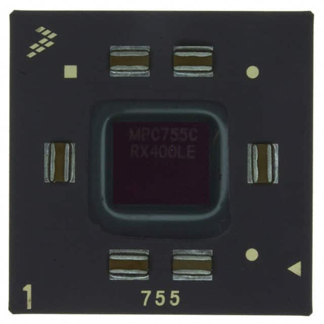
- Part No.:
- MPC7410HX400LE
- Manufacturer:
- NXP Semiconductors
- Category:
- Microprocessors
- Package:
- 360-BCBGA, FCCBGA
- Datasheet:
-
 MPC7410HX400LE.pdf
- Description:
- IC MPU MPC74XX 400MHZ 360CBGA
- Quantity:
- Payment:

- Shipping:

Inventory:1,919
Please send an inquiry. Send us your inquiry, and we will respond immediately.
Product details
Overview
MPC7410HX400LE from Freescale Semiconductor is a 400 MHz PowerPC G4 RISC microprocessor implementing the full 32-bit PowerPC architecture with AltiVec™ SIMD engine, 32 KB L1 instruction and data caches, integrated L2 cache controller, and MPX bus interface - deployed in high-performance embedded computing, digital signal processing, and telecom infrastructure systems.
For engineers reviewing the MPC7410HX400LE datasheet, MPC7410HX400LE pinout, MPC7410HX400LE application, or MPC7410HX400LE equivalent, key selection considerations include its 400 MHz core frequency, 1.8 V core supply, 360-ball CBGA package, AltiVec acceleration capability, and support for 512 KB–2 MB external L2 SRAM configurations.
Technical Context
The MPC7410HX400LE implements a deeply pipelined, out-of-order execution core with dual fixed-point units (FXU1/FXU2), a three-stage floating-point unit supporting IEEE 754 single/double precision at 3-cycle latency, and a dedicated 128-bit AltiVec unit comprising permute and ALU subunits with 32×128-bit vector register file.
Its memory subsystem features nonblocking 32 KB eight-way set-associative L1 I/D caches, hardware-managed 128-entry ITLB/DTLB, configurable L2 interface supporting 32-/64-/128-byte line sizes, and a 64-bit MPX bus with selectable 1.8 V / 2.5 V / 3.3 V I/O voltage thresholds controlled by BVSEL/L2VSEL pins sampled at HRESET negation.
Key Specifications
| Parameter | Value and Actual Design Meaning |
|---|---|
| Core Frequency | 400 MHz - guaranteed maximum operating frequency under recommended thermal and voltage conditions. |
| Core Supply Voltage | 1.8 V ± 100 mV - low-voltage core enabling reduced dynamic power and thermal density in high-clock designs. |
| L1 Cache | 32 KB instruction + 32 KB data, eight-way set-associative - enables single-cycle access and supports AltiVec LRU algorithms. |
| L2 Interface | 64-bit data bus, 19-bit address bus, 32/64/128-byte line sizes - supports up to 2 MB two-way set-associative external SRAM with direct-mapped mode option. |
| AltiVec Engine | Full 128-bit SIMD unit with dedicated permute and ALU pipelines - accelerates media, signal, and scientific workloads without software emulation overhead. |
| Bus Interface | MPX extension of 60x bus, 32-bit address/64-bit data, 2×–9× core-to-bus multipliers - maintains compatibility while enabling scalable bandwidth for memory-intensive applications. |
| Power Modes | Doze, Nap, Sleep (with PLL/DLL disable) - lowest sleep mode draws ≤1.1 W typical, enabling thermal management in fanless enclosures. |
Pinout & Package
Package: 360-ball Ceramic Ball Grid Array (CBGA), 27 mm × 27 mm, 1.27 mm pitch, RoHS-compliant lead-free C5 spheres. Thermal resistance: RθJA = 18°C/W (natural convection, 4-layer board).
| Pin/Terminal | Circuit Role | Design Meaning |
|---|---|---|
| HRESET | Asynchronous reset input | Active-low global reset; samples BVSEL/L2VSEL at negation to configure I/O voltage thresholds. |
| SYSCLK | Primary clock input | Differential-capable single-ended input; defines base timing for PLL multiplication to 400 MHz core frequency. |
| PLL_CFG[0:3] | PLL configuration inputs | Four-pin strap determining VCO multiplier ratio; must match 400 MHz target and SYSCLK frequency per Table 7. |
| OVDD / L2OVDD | I/O power supplies | Separate 1.8/2.5/3.3 V supplies for processor and L2 buses; L2OVDD required even if L2 interface unused. |
| TCK/TMS/TDI/TDO | JTAG boundary scan | IEEE 1149.1 compliant test interface; operates at 1.8 V logic levels regardless of BVSEL setting during EXTEST/CLAMP. |
Key Features
| Feature | Design Value |
|---|---|
| AltiVec SIMD Engine | Hardware-accelerated 128-bit vector processing with dedicated permute and ALU units - eliminates software loop overhead for pixel, audio, and radar signal processing. |
| Out-of-Order Execution | Eight-entry completion queue and up to eight concurrent dispatch slots - sustains two instructions per cycle throughput despite pipeline stalls and cache misses. |
| L2 Cache Controller | Configurable interface supporting 512 KB–2 MB external SRAM with selectable line size and direct-mapped mode - enables deterministic latency tuning for real-time DSP tasks. |
| Power Management | Three static low-power states (Doze/Nap/Sleep) plus dynamic voltage scaling - reduces active power to ≤5.3 W typical at 400 MHz while maintaining full architectural state. |
| Memory Coherency | Five-state MESI+ protocol with shared intervention - ensures cache coherency across multiple MPC7410HX400LE processors in symmetric multiprocessing systems. |
Applications
| Telecom Baseband Processing | Digital Signal Processing |
|---|---|
Use Scenario: Real-time channel coding, FFT-based modulation, and packet classification in 3G/4G radio base stations. IC Role / Device Role / Timing Role: Primary compute engine executing AltiVec-optimized signal processing kernels with deterministic interrupt latency. Use Value: 400 MHz AltiVec throughput delivers >1.2 GOPS on 16-bit integer operations - meets 3GPP TS 25.222 latency requirements for turbo decoding. | Use Scenario: High-fidelity audio mixing, noise cancellation, and beamforming in professional audio DSP platforms. IC Role / Device Role / Timing Role: Host processor managing DMA transfers to external audio codecs while running real-time FIR/IIR filters in L1 cache. Use Value: Nonblocking L1/L2 caches and 64-bit MPX bus sustain 1.8 GB/s sustained memory bandwidth - prevents sample dropouts at 192 kHz/24-bit stereo. |
| Industrial Control Systems | Avionics Data Acquisition |
Use Scenario: Motion control coordination, safety-critical PLC logic execution, and EtherCAT master timing in factory automation. IC Role / Device Role / Timing Role: Deterministic real-time controller with hardware timer, performance monitor, and JTAG debug support. Use Value: Five-state cache coherency and 128-entry TLB enable <1 µs context switch time - satisfies IEC 61131-3 cycle time requirements for motion profiles. | Use Scenario: Sensor fusion, inertial navigation computation, and ARINC 429/664 interface management in flight data recorders. IC Role / Device Role / Timing Role: Radiation-tolerant compute node performing Kalman filtering and fault detection using ECC-protected L1/L2 paths. Use Value: Parity-checked 60x and L2 buses plus ABIST factory test ensure >10⁹ MTBF - meets DO-254 Level A design assurance for critical avionics functions. |
Equivalent & Alternatives
The following parts are listed as comparable options for similar RISC microprocessor applications.
| Alternative Part | Technical Difference | Application Difference | Selection Advice |
|---|---|---|---|
| MPC7410HX450LE | 450 MHz core, identical pinout and feature set, higher thermal envelope (10.7 W max) | Requires enhanced cooling but delivers 12.5% higher integer/FPU throughput | Select when system thermal design supports ≥20°C/W RθJA and benchmarking shows CPU-bound bottlenecks. |
| MPC7450MX500LE | 500 MHz core, added 64-bit addressing, larger L2 controller, same CBGA package | Supports >4 GB physical memory and larger L2 configurations (up to 4 MB) | Choose for next-generation designs requiring extended virtual memory space and higher sustained bandwidth. |
Compared with MPC7410HX400LE, the MPC7410HX450LE offers higher clock speed within identical thermal/power constraints, while the MPC7450MX500LE extends memory addressing and L2 scalability - both retain AltiVec, MPX bus, and JTAG compatibility but require validation of voltage regulator and heatsink margins.
Availability
MPC7410HX400LE is available at Aetrix Electronics and suitable for telecom infrastructure, industrial control, and avionics applications requiring stable component supply, long-lifecycle support, and traceable sourcing for legacy system maintenance.
Supply support for MPC7410HX400LE includes scheduled delivery planning, volume procurement assistance, BOM continuity management, traceable sourcing, and lifecycle availability coordination for OEM customers, industrial embedded developers, connected-device designers, and electronics production programs.
Manufacturer
Freescale Semiconductor (now part of NXP Semiconductors) is a fabless semiconductor company specializing in embedded processing, analog, and connectivity solutions for automotive, industrial, and networking markets.
The MPC7410HX400LE belongs to Freescale's PowerPC G4 family, designed specifically for high-performance embedded computing where AltiVec acceleration, deterministic real-time response, and scalable memory subsystems are critical.
FAQ
What is the maximum guaranteed operating frequency of the MPC7410HX400LE?
The MPC7410HX400LE is binned and tested to operate reliably at a maximum core frequency of 400 MHz under recommended conditions (1.8 V ±100 mV, Tj ≤ 105°C). This rating is verified via functional testing at speed using contrived instruction sequences that maximize execution unit utilization, and it corresponds to a minimum SYSCLK frequency of 33 MHz with appropriate PLL_CFG[0:3] settings per Table 7 of the hardware specifications.
Does the MPC7410HX400LE support 3.3 V I/O signaling on its processor bus?
Yes, the MPC7410HX400LE supports 3.3 V I/O signaling on the processor bus when BVSEL is configured to ¬HRESET or 1, as specified in Table 2 and Table 3 of the hardware specifications. This capability is available only on Mxx7410xxnnnLE revision 1.4 and later; earlier revisions limit OVDD to 2.5 V maximum and do not support the 3.3 V threshold mode.
How does the MPC7410HX400LE handle L2 cache coherency in multiprocessor systems?
The MPC7410HX400LE implements a five-state cache coherency protocol (MESI plus shared intervention) that maintains consistency across multiple processors sharing the same L2 cache domain. This protocol is executed entirely in hardware and requires no software intervention, enabling symmetric multiprocessing configurations where each MPC7410HX400LE maintains independent L1 caches while coordinating castout and snoop actions over the MPX bus.
What thermal management provisions are built into the MPC7410HX400LE?
The MPC7410HX400LE integrates three static power-saving modes (Doze, Nap, Sleep), dynamic voltage scaling, and thermal monitoring circuitry. Its 0.18 µm CMOS process and 1.8 V core reduce intrinsic power dissipation, while the CBGA package provides low RθJC (<0.1°C/W) and documented RθJA values (18°C/W natural convection) to guide heatsink selection. The die-junction temperature sensor feeds into the performance monitor unit for closed-loop thermal throttling.
Can the MPC7410HX400LE execute legacy PowerPC 603/604 code without modification?
Yes, the MPC7410HX400LE fully implements the PowerPC 32-bit architecture including all Book III-S and Book III-E specifications, ensuring binary compatibility with software written for earlier PowerPC processors such as the MPC603e and MPC604. Its instruction set includes backward-compatible scalar, FPU, and MMU functionality, while AltiVec instructions are optional extensions that do not affect execution of legacy code paths.
MPC7410HX400LE Specifications
- Product attributes
- Attribute value
- Manufacturer:
- NXP Semiconductors
- Package/Case:
- 360-BCBGA, FCCBGA
- Series:
- MPC74xx
- Packaging:
- Tray
- Product Status:
- Obsolete
- Core Processor:
- PowerPC G4
- Number of Cores/Bus Width:
- 1 Core, 32-Bit
- Speed:
- 400MHz
- Co-Processors/DSP:
- -
- RAM Controllers:
- -
- Graphics Acceleration:
- No
- Display & Interface Controllers:
- -
- Ethernet:
- -
- SATA:
- -
- USB:
- -
- Voltage - I/O:
- 1.8V, 2.5V, 3.3V
- Operating Temperature:
- 0°C ~ 105°C (TA)
- Grade:
- -
- Qualification:
- -
- Security Features:
- -
- Mounting Type:
- Surface Mount
- Supplier Device Package:
- 360-CBGA (25x25)
- Additional Interfaces:
- -
MPC7410HX400LE FAQ
1.How can I place an order for MPC7410HX400LE through Aetrix?
Please submit a Request for Quotation (RFQ) for MPC7410HX400LE on Aetrix. Our sales agent will provide a competitive quotation and guide you through the order confirmation once you accept the terms.
2.Are the price and stock information for MPC7410HX400LE reliable?
The price and inventory of MPC7410HX400LE are updated periodically and may fluctuate due to market conditions. Stock and pricing data are typically refreshed every 24 hours. Quotation validity for MPC7410HX400LE is usually 5 days.
3.What payment methods are accepted for MPC7410HX400LE?
We accept Wire Transfer, PayPal, Credit Card, Western Union, MoneyGram, and Escrow for MPC7410HX400LE transactions.
Note: Certain payment methods may incur a processing fee.
4.How is shipping managed for MPC7410HX400LE?
MPC7410HX400LE orders can be shipped via leading logistics carriers, including DHL, UPS, FedEx, TNT, or Registered Mail.
Once your MPC7410HX400LE order is processed, you will receive an email with the shipment details and tracking number.
Note: Tracking information may take up to 24 hours to appear. Express delivery typically takes 3–5 business days.
5.How can I obtain technical support or documentation for MPC7410HX400LE?
For technical support, including MPC7410HX400LE datasheets, pinout diagrams, or application guidance, please contact our engineering support team. They can provide detailed documentation and assistance for your MPC7410HX400LE requirements.
6.How does Aetrix verify that MPC7410HX400LE is sourced from the original manufacturer or authorized distributors?
All MPC7410HX400LE products on Aetrix are procured from qualified distributors and authorized channels. Our dedicated quality assurance team conducts strict verification, including traceability checks and, if necessary, third-party testing. This ensures that MPC7410HX400LE meets industry standards.
7.What is the process for return or replacement of MPC7410HX400LE?
All MPC7410HX400LE units undergo pre-shipment inspection (PSI). If there is an issue with MPC7410HX400LE, returns or replacements are accepted under the following conditions:
1.Quantity discrepancies, incorrect items, or visible external defects (such as breakage or corrosion), acknowledged by Aetrix.
2.The issue is reported within 90 days of delivery.
3.The MPC7410HX400LE part is unused and in its original packaging.
Return procedure for MPC7410HX400LE:
1.Submit a request within 90 days.
2.Obtain a Return Material Authorization (RMA) from Aetrix.
MPC7410HX400LE Tags

-
AT91SAM9260B-CU-999
Microchip Technology
-
AT91SAM9G25-CU
Microchip Technology

-
ATSAMA5D27C-CU
Microchip Technology
-
AT91SAM9X35-CU
Microchip Technology
-
AT91SAM9X25-CU
Microchip Technology

-
MCIMX6Y2CVM08AB
NXP Semiconductors
.JPG)
-
AM3352BZCZ100
Texas Instruments
-
AT91SAM9260B-CU
Microchip Technology

-
AT91SAM9260B-QU
Microchip Technology

-
ATSAMA5D31A-CU
Microchip Technology
-
AT91SAM9G20B-CU-999
Microchip Technology
-
MCIMX6Y2CVM05AB
NXP Semiconductors
Tech Hub

A practical engineering guide to 3.3V and 5V logic compatibility, input thresholds, resistor dividers, translator ICs, MOSFET level shifting, I2C pull-ups, timing limits and power-sequencing risks.

The 74HC595 uses push-pull logic outputs, while the TPIC6B595 uses 50 V open-drain DMOS sinks for higher-power loads. This guide compares timing, current limits, 3.3 V interfacing, load wiring, thermal…

The 74HC595 converts serial data into eight stable parallel outputs. This guide covers pin functions, shift and storage timing, OE and MR behavior, drive-current limits, cascading, voltage compatibilit…

A technical comparison of level-sensitive latches and edge-triggered flip-flops, covering timing windows, setup and hold limits, master–slave operation, time borrowing, race-through, HDL inference and…

A D latch stores one bit while Enable controls when data can pass. This reference covers gate-level operation, truth tables, transparency, setup and hold timing, LE versus OE, common ICs and practical …

An SR latch stores one bit through cross-coupled feedback. This engineering reference covers NOR and NAND implementations, truth tables, forbidden-state recovery, gated operation, switch debouncing, fa…

Latch circuits retain one bit through feedback. This technical reference covers SR and D latches, truth tables, transparency, timing limits, latch-versus-flip-flop behavior, applications and common log…

An engineering guide to LED driver operation, constant-current and constant-voltage outputs, linear and switching topologies, dimming, IC selection, calculations, replacement compatibility, and fault c…

Operational amplifier guide covering op amp basics, feedback, ideal vs real op amps, common configurations, buffer circuits, offset, bias current, gain-bandwidth, slew rate, rail-to-rail limits and sel…

Jumper cables guide covering safe connection order, red and black clamp placement, final ground connection, cable gauge, length, clamp quality, copper vs CCA cables, jump starter comparison and battery…


