
 My Inquiry
 My Account


NXP Semiconductors MPC850DECVR66BU
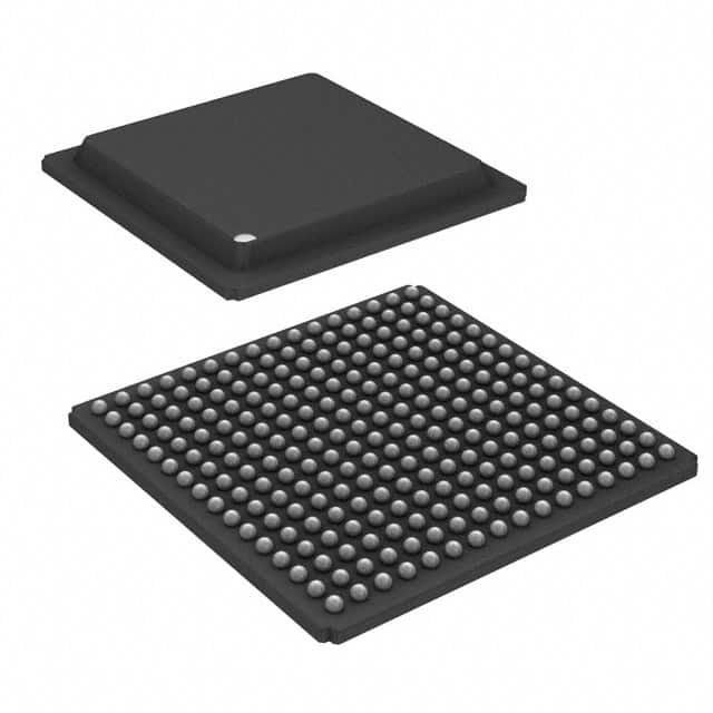
- Part No.:
- MPC850DECVR66BU
- Manufacturer:
- NXP Semiconductors
- Category:
- Microprocessors
- Package:
- 256-BBGA
- Datasheet:
-
 MPC850DECVR66BU.pdf
- Description:
- IC MPU MPC8XX 66MHZ 256BGA
- Quantity:
- Payment:

- Shipping:

Inventory:1,722
Please send an inquiry. Send us your inquiry, and we will respond immediately.
Product details
Overview
MPC850DECVR66BU from Freescale Semiconductor is a PowerQUICC™ integrated communications processor combining an embedded 32-bit MPC8xx core with a dedicated RISC communications processor (CP), dual-port RAM (8 KB), Ethernet MAC, USB 1.1 controller, two SCCs, two SMCs, SPI, I²C, and PCMCIA-ATA interface - designed for cost-sensitive remote-access and telecom edge devices operating at up to 66 MHz core frequency.
For engineers reviewing the MPC850DECVR66BU datasheet, MPC850DECVR66BU pinout, MPC850DECVR66BU application, or MPC850DECVR66BU equivalent, key selection considerations include its dual-SCC Ethernet/HDLC support, USB host/slave capability, 3.3-V operation with 5-V-tolerant I/O, BGA-352 package, and requirement for half-speed bus configuration (33 MHz) when running at 66 MHz core clock.
Technical Context
The MPC850DECVR66BU implements a split-processor architecture: the main MPC8xx core handles system control and application tasks, while the independent 32-bit Harvard-architecture communications processor (CP) offloads serial protocol processing (Ethernet, HDLC, USB, UART, SPI, I²C) using 8 KB of on-chip dual-port RAM and 20 SDMA channels. It supports IEEE 802.3 10-Mbps Ethernet via SCC1/SCC2 and full-duplex USB 1.1 at 1.5/12 Mbps.
Its memory subsystem includes an eight-bank programmable controller supporting SDRAM, SRAM, Flash, and EPROM with boot-selectable 8/16/32-bit interfaces; bus timing requires external configuration via UPM (User Programmable Machine) microcode, and the device mandates half-speed bus operation (33 MHz) when the core runs at 66 MHz - confirmed in Table 6 timing specifications for 66 MHz mode.
Key Specifications
| Parameter | Value and Actual Design Meaning |
|---|---|
| Core Architecture | 32-bit PowerPC MPC8xx single-issue core with 2-KB instruction cache and 1-KB data cache |
| Max Core Frequency | 66 MHz - requires bus clock configured to 33 MHz (half-speed mode) per timing spec B1–B30 |
| Communications Peripherals | Two SCCs (Ethernet/HDLC), one USB 1.1 controller, two SMCs, SPI, I²C, time slot assigner |
| Dual-Port RAM | 8 KB - shared between core and CP for descriptor and packet buffering |
| I/O Voltage Tolerance | 5-V tolerant on all general-purpose I/O pins - enables direct interfacing with legacy 5-V logic |
| Package | BGA-352 - 352-ball fine-pitch ball grid array with θJA = 31°C/W (multilayer board w/ thermal vias) |
| Supply Voltage Range | 3.135 V to 3.465 V at ≥40 MHz - strict regulation required to meet AC timing margins |
Pinout & Package
Package: 352-ball PBGA (Plastic Ball Grid Array), 27 mm × 27 mm, 1.27 mm pitch, RoHS-compliant. Thermal pad on underside requires soldered thermal connection to internal ground plane.
| Pin/Terminal | Circuit Role | Design Meaning |
|---|---|---|
| VDDH / VDDL / KAPWR / VDDSYN | Core & I/O power supply inputs | Four independent 3.3-V supplies - must be decoupled separately with ≥4× 0.1 µF capacitors near package edges |
| EXTCLK / EXTAL | External clock input / crystal oscillator input | Accepts 33–66 MHz external clock or 33–66 MHz crystal; phase jitter ≤2.0 ns (B1c–B1d) critical for CPM stability |
| CLKOUT | Generated system clock output | Buffered derivative of internal PLL; 33 MHz output when core runs at 66 MHz; rise/fall time ≤4 ns (B4–B5) |
| A[6–31] / D[0–31] | Address and data bus signals | 32-bit multiplexed address/data bus - requires external latch (e.g., 74LVC573) and careful trace length control (≤6 inches) |
| TS / TA / TEA / BB / BI / BR / BG | Bus control and strobe signals | Asynchronous bus handshaking - timing validated only for GPCM mode with FFACT = 0.250–1.500 per Table 6 |
| SCC1_TXD / SCC1_RXD / SCC2_TXD / SCC2_RXD | Ethernet physical layer interface | Differential pairs for 10BASE-T MII or RMII - require 50-Ω controlled impedance routing and transformer coupling |
| USBTXP / USBTXN / USBRXP / USBRXN | USB 1.1 differential transceiver I/O | Full-speed (12 Mbps) or low-speed (1.5 Mbps) signaling - needs 90-Ω differential pair routing and ESD protection |
Key Features
| Feature | Design Value |
|---|---|
| Dedicated Communications Processor (CP) | Offloads Ethernet, HDLC, USB, and serial protocol processing from main core - reduces CPU utilization by >40% in multi-channel telecom gateways |
| Two SCCs with IEEE 802.3 Support | Enables dual-port 10-Mbps Ethernet bridging or router functions without external PHYs beyond magnetics |
| USB 1.1 Host/Slave Controller | Eliminates need for external USB interface IC in remote terminal units and DSL modems |
| PCMCIA-ATA Interface (Release 2.1) | Direct attachment of CompactFlash or ATA hard drives - simplifies field-upgradable storage in network appliances |
| Programmable Memory Controller | Supports mixed-memory systems (SDRAM + Flash + SRAM) with bank-specific timing - avoids glue logic in BOM |
| IEEE 1149.1 JTAG Debug Port | Enables boundary-scan testing and real-time core/CP debugging without halting communications traffic |
Applications
| DSL Access Multiplexer (DSLAM) Line Card | Industrial Ethernet Gateway |
|---|---|
Use Scenario: Aggregating multiple ADSL2+ subscriber lines into a Gigabit Ethernet uplink in carrier-class DSLAM chassis. IC Role / Device Role / Timing Role: MPC850DECVR66BU serves as line-card controller - managing ATM/PTM framing, QoS scheduling, and Ethernet MAC bridging via dual SCCs and USB-based management interface. Use Value: Dual SCCs enable simultaneous upstream/downstream HDLC framing; 8-KB dual-port RAM buffers per-line packet descriptors; 66-MHz core sustains 200+ concurrent PPPoE sessions. |
Use Scenario: Protocol translation between Modbus RTU field devices and EtherNet/IP control networks in factory automation. IC Role / Device Role / Timing Role: MPC850DECVR66BU acts as real-time protocol gateway - running Modbus master over SMC UARTs while bridging to EtherNet/IP via SCC1 Ethernet MAC. Use Value: Independent CP handles serial protocol state machines without CPU intervention; 33-MHz bus timing ensures deterministic response under 10-ms cycle times. |
| Remote Terminal Unit (RTU) for SCADA | VoIP Terminal Adapter |
Use Scenario: Oil/gas pipeline monitoring unit collecting sensor data via RS-485 and transmitting alarms over PSTN or cellular backhaul. IC Role / Device Role / Timing Role: MPC850DECVR66BU functions as embedded controller - executing SCADA firmware on MPC8xx core while CP manages HDLC telemetry frames and USB-connected modem. Use Value: Hardware CRC generation in SCCs ensures bit-error-free telemetry; 5-V-tolerant I/O interfaces directly with legacy RS-485 transceivers; low-power stop mode extends battery life. |
Use Scenario: Residential VoIP adapter converting analog POTS lines to SIP-over-Ethernet using onboard DSP and voice codec. IC Role / Device Role / Timing Role: MPC850DECVR66BU provides system control and peripheral bridging - hosting SIP stack on core while CP handles PCM audio streaming via TDM-aligned SMCs and SPI-connected codec. Use Value: Time slot assigner routes 8-channel PCM between SMCs and SCCs; USB port enables firmware updates via flash drive; PCMCIA socket supports optional Wi-Fi module. |
Equivalent & Alternatives
The following parts are listed as comparable options for similar integrated communications processor applications.
| Alternative Part | Technical Difference | Application Difference | Selection Advice |
|---|---|---|---|
| MPC850DEVR66B | Same core/peripheral set but BGA-352 package with different thermal pad layout and JEDEC MO-251 footprint variant | Identical functional use; requires PCB redesign due to ball map shift in power/ground ball placement | Select when sourcing from alternate Freescale wafer lots requiring mechanical compatibility verification |
| MPC860TVR66D | Higher-performance MPC860 core (66 MHz), adds QUICC Engine microcode acceleration, larger 4-KB DPRAM, no USB support | Better suited for high-throughput HDLC/ATM applications; lacks USB and PCMCIA - unsuitable for field-upgradeable designs | Choose for telecom infrastructure where USB/PCMCIA are unnecessary and CPM throughput >150 Mbps is required |
Compared with MPC850DECVR66BU, MPC850DEVR66B offers identical functionality with mechanical rework needed, while MPC860TVR66D trades USB/PCMCIA for higher CPM bandwidth and no USB - making it optimal for pure telecom line cards but incompatible with USB-dependent field service workflows.
Availability
MPC850DECVR66BU is available at Aetrix Electronics and suitable for DSLAM line cards, industrial Ethernet gateways, remote terminal units (RTUs), VoIP adapters, and SCADA edge controllers requiring stable component supply across extended product lifecycles.
Supply support for MPC850DECVR66BU includes scheduled delivery planning, volume procurement assistance, BOM continuity management, traceable sourcing, and lifecycle availability coordination for OEM customers, industrial embedded developers, connected-device designers, and electronics production programs.
Manufacturer
Freescale Semiconductor (now part of NXP Semiconductors since 2015) was a pioneer in PowerPC-based communications processors, delivering high-integration SoCs for networking and telecom infrastructure.
The MPC850 family was engineered specifically for cost-sensitive, low-power remote access and telecommunications edge devices - integrating Ethernet, USB, HDLC, and PCMCIA into a single chip to replace multi-chip controller solutions.
FAQ
What is the maximum supported bus speed for MPC850DECVR66BU at 66 MHz core frequency?
The MPC850DECVR66BU must operate in half-speed bus mode when the core runs at 66 MHz, limiting the external bus clock to 33 MHz. This is explicitly mandated in Section 6 ("Bus Signal Timing") of the hardware specifications - Table 6 lists timing parameters only for 50/66/80 MHz core speeds with corresponding 25/33/40 MHz bus rates. Attempting full-speed 66 MHz bus operation violates setup/hold timing (e.g., B18–B21) and risks data corruption.
Does MPC850DECVR66BU support USB 2.0?
No, MPC850DECVR66BU integrates a USB 1.1 controller compliant with USB Specification Revision 1.1, supporting only low-speed (1.5 Mbps) and full-speed (12 Mbps) modes. It does not implement USB 2.0 high-speed (480 Mbps) transceivers, PHY, or protocol engine - confirmed by absence of UTMI+ interface signals and USB 2.0 descriptors in all documentation, including the MPC850EC Rev. 2 datasheet.
How is Ethernet connectivity implemented on MPC850DECVR66BU?
MPC850DECVR66BU implements Ethernet at the MAC layer via two Serial Communications Controllers (SCCs), each supporting IEEE 802.3 10-Mbps baseband operation. It requires external PHY devices (e.g., DP83843 or LAN83C185) and magnetics for physical layer connectivity. The SCCs handle frame assembly/disassembly, CRC generation/checking, and MII/RMII signaling - no integrated PHY is present on-die.
What power supply sequencing is required for MPC850DECVR66BU?
MPC850DECVR66BU requires simultaneous ramp-up of all four power domains (VDDH, VDDL, KAPWR, VDDSYN) within ±100 ms of each other, with no voltage exceeding another by more than 0.3 V during startup. Asymmetric sequencing or >0.3 V differentials between supplies may cause latch-up or undefined reset behavior - specified in Section 5 ("Power Considerations") and reinforced by absolute maximum ratings in Table 2.
Is MPC850DECVR66BU pin-compatible with MPC850SR or MPC850DSL variants?
No, MPC850DECVR66BU is not pin-compatible with MPC850SR or MPC850DSL. While all share the BGA-352 package, Table 1 ("MPC850 Functionality Matrix") confirms differing peripheral configurations: MPC850DECVR66BU has two SCCs and USB support but no ATM capability, whereas MPC850SR/DSL add UTOPIA ports and ATM support - requiring distinct pin allocations for UTOPIA signals (TxDAT, RxDAT, etc.) absent in MPC850DECVR66BU's signal list.
MPC850DECVR66BU Specifications
- Product attributes
- Attribute value
- Manufacturer:
- NXP Semiconductors
- Package/Case:
- 256-BBGA
- Series:
- MPC8xx
- Packaging:
- Tray
- Product Status:
- Obsolete
- Core Processor:
- MPC8xx
- Number of Cores/Bus Width:
- 1 Core, 32-Bit
- Speed:
- 66MHz
- Co-Processors/DSP:
- Communications; CPM
- RAM Controllers:
- DRAM
- Graphics Acceleration:
- No
- Display & Interface Controllers:
- -
- Ethernet:
- 10Mbps (1)
- SATA:
- -
- USB:
- USB 1.x (1)
- Voltage - I/O:
- 3.3V
- Operating Temperature:
- -40°C ~ 95°C (TA)
- Grade:
- -
- Qualification:
- -
- Security Features:
- -
- Mounting Type:
- Surface Mount
- Supplier Device Package:
- 256-PBGA (23x23)
- Additional Interfaces:
- HDLC/SDLC, I2C, IrDA, PCMCIA-ATA, TDM, UART/USART
MPC850DECVR66BU FAQ
1.How can I place an order for MPC850DECVR66BU through Aetrix?
Please submit a Request for Quotation (RFQ) for MPC850DECVR66BU on Aetrix. Our sales agent will provide a competitive quotation and guide you through the order confirmation once you accept the terms.
2.Are the price and stock information for MPC850DECVR66BU reliable?
The price and inventory of MPC850DECVR66BU are updated periodically and may fluctuate due to market conditions. Stock and pricing data are typically refreshed every 24 hours. Quotation validity for MPC850DECVR66BU is usually 5 days.
3.What payment methods are accepted for MPC850DECVR66BU?
We accept Wire Transfer, PayPal, Credit Card, Western Union, MoneyGram, and Escrow for MPC850DECVR66BU transactions.
Note: Certain payment methods may incur a processing fee.
4.How is shipping managed for MPC850DECVR66BU?
MPC850DECVR66BU orders can be shipped via leading logistics carriers, including DHL, UPS, FedEx, TNT, or Registered Mail.
Once your MPC850DECVR66BU order is processed, you will receive an email with the shipment details and tracking number.
Note: Tracking information may take up to 24 hours to appear. Express delivery typically takes 3–5 business days.
5.How can I obtain technical support or documentation for MPC850DECVR66BU?
For technical support, including MPC850DECVR66BU datasheets, pinout diagrams, or application guidance, please contact our engineering support team. They can provide detailed documentation and assistance for your MPC850DECVR66BU requirements.
6.How does Aetrix verify that MPC850DECVR66BU is sourced from the original manufacturer or authorized distributors?
All MPC850DECVR66BU products on Aetrix are procured from qualified distributors and authorized channels. Our dedicated quality assurance team conducts strict verification, including traceability checks and, if necessary, third-party testing. This ensures that MPC850DECVR66BU meets industry standards.
7.What is the process for return or replacement of MPC850DECVR66BU?
All MPC850DECVR66BU units undergo pre-shipment inspection (PSI). If there is an issue with MPC850DECVR66BU, returns or replacements are accepted under the following conditions:
1.Quantity discrepancies, incorrect items, or visible external defects (such as breakage or corrosion), acknowledged by Aetrix.
2.The issue is reported within 90 days of delivery.
3.The MPC850DECVR66BU part is unused and in its original packaging.
Return procedure for MPC850DECVR66BU:
1.Submit a request within 90 days.
2.Obtain a Return Material Authorization (RMA) from Aetrix.
MPC850DECVR66BU Tags

-
AT91SAM9260B-CU-999
Microchip Technology
-
AT91SAM9G25-CU
Microchip Technology

-
ATSAMA5D27C-CU
Microchip Technology
-
AT91SAM9X35-CU
Microchip Technology
-
AT91SAM9X25-CU
Microchip Technology

-
MCIMX6Y2CVM08AB
NXP Semiconductors
.JPG)
-
AM3352BZCZ100
Texas Instruments
-
AT91SAM9260B-CU
Microchip Technology

-
AT91SAM9260B-QU
Microchip Technology

-
ATSAMA5D31A-CU
Microchip Technology
-
AT91SAM9G20B-CU-999
Microchip Technology
-
MCIMX6Y2CVM05AB
NXP Semiconductors
Tech Hub

A practical engineering guide to 3.3V and 5V logic compatibility, input thresholds, resistor dividers, translator ICs, MOSFET level shifting, I2C pull-ups, timing limits and power-sequencing risks.

The 74HC595 uses push-pull logic outputs, while the TPIC6B595 uses 50 V open-drain DMOS sinks for higher-power loads. This guide compares timing, current limits, 3.3 V interfacing, load wiring, thermal…

The 74HC595 converts serial data into eight stable parallel outputs. This guide covers pin functions, shift and storage timing, OE and MR behavior, drive-current limits, cascading, voltage compatibilit…

A technical comparison of level-sensitive latches and edge-triggered flip-flops, covering timing windows, setup and hold limits, master–slave operation, time borrowing, race-through, HDL inference and…

A D latch stores one bit while Enable controls when data can pass. This reference covers gate-level operation, truth tables, transparency, setup and hold timing, LE versus OE, common ICs and practical …

An SR latch stores one bit through cross-coupled feedback. This engineering reference covers NOR and NAND implementations, truth tables, forbidden-state recovery, gated operation, switch debouncing, fa…

Latch circuits retain one bit through feedback. This technical reference covers SR and D latches, truth tables, transparency, timing limits, latch-versus-flip-flop behavior, applications and common log…

An engineering guide to LED driver operation, constant-current and constant-voltage outputs, linear and switching topologies, dimming, IC selection, calculations, replacement compatibility, and fault c…

Operational amplifier guide covering op amp basics, feedback, ideal vs real op amps, common configurations, buffer circuits, offset, bias current, gain-bandwidth, slew rate, rail-to-rail limits and sel…

Jumper cables guide covering safe connection order, red and black clamp placement, final ground connection, cable gauge, length, clamp quality, copper vs CCA cables, jump starter comparison and battery…


