
 My Inquiry
 My Account


Microchip Technology MPL360B-I/Y8X
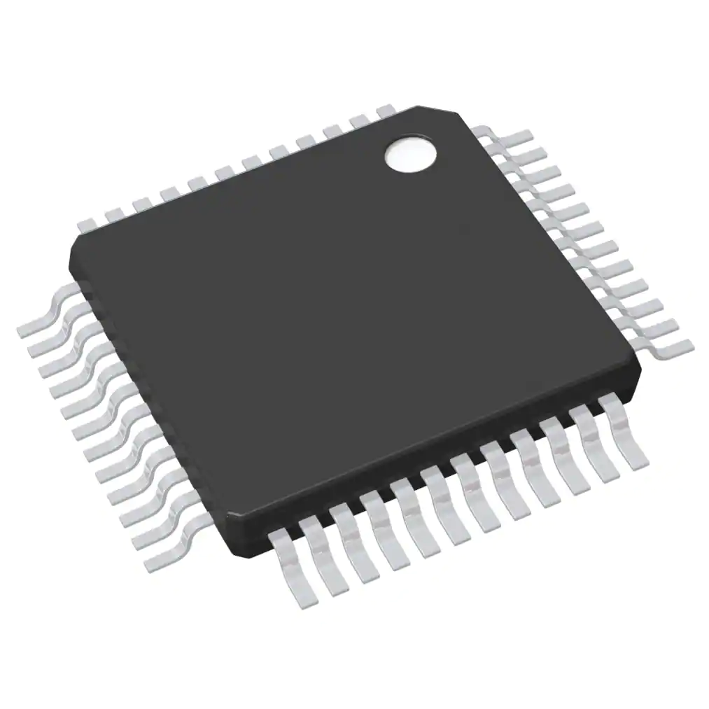
- Part No.:
- MPL360B-I/Y8X
- Manufacturer:
- Microchip Technology
- Category:
- Telecom
- Package:
- 48-TQFP
- Datasheet:
-
 MPL360B-I/Y8X.pdf
- Description:
- IC TELECOM INTERFACE 48TQFP
- Quantity:
- Payment:

- Shipping:

Inventory:4,307
Please send an inquiry. Send us your inquiry, and we will respond immediately.
Product details
Overview
MPL360B-I/Y8X from Microchip Technology is a programmable narrow-band Power Line Communication (PLC) modem IC supporting ITU G.9903 (G3-PLC®), ITU G.9904 (PRIME), and custom PLC protocols below 500 kHz. It integrates ARM Cortex-M7 core (216 MHz), 192 kB SRAM, cryptographic engine (AES-128/192/256), and analog front-end with PGA, ADC, DAC, and dual transmission branches. It operates from 3.3 V I/O and 1.25 V core supply, targeting smart metering and IoT energy infrastructure.
For engineers reviewing the MPL360B-I/Y8X datasheet, MPL360B-I/Y8X pinout, MPL360B-I/Y8X application, or MPL360B-I/Y8X equivalent, this page delivers verified technical context, exact pin functions for SPI-controlled PLC transceiver design, zero-cross detection integration, AGC-driven signal conditioning, and secure boot implementation details - all specific to the MPL360B-I/Y8X QFN-48 variant.
Technical Context
The MPL360B-I/Y8X implements a hybrid architecture combining an ARM Cortex-M7 CPU (216 MHz) with dedicated co-processors and hardware accelerators for narrow-band PLC signal processing, enabling real-time modulation/demodulation of G3-PLC® and PRIME waveforms. Its analog front-end includes a PGA with automatic gain control, 12-bit ADC, DAC, and two independent transmission drivers (EMIT[0:3], TXRX0/TXRX1) supporting direct line driving or external Class-D amplification.
It relies on external host microcontroller coordination via 4-line SPI (NPCS0, SPCK, MOSI, MISO), with NRST and LDO ENABLE for system-level control. Zero-cross detection (VZC) and carrier-detect interrupt capability support synchronized PLC burst transmission aligned to AC mains phase - critical for CENELEC EN50065-compliant smart grid deployments.
Key Specifications
| Parameter | Value and Actual Design Meaning |
|---|---|
| PLC Bandwidth | Up to 500 kHz - enables compliance with CENELEC A/B/C, FCC Part 15, ARIB STD-T108, and KN60 spectral masks. |
| CPU Core | ARM Cortex-M7 @ 216 MHz - provides deterministic real-time execution for protocol stack processing and firmware updates. |
| On-chip Memory | 192 kB SRAM (code + data) - sufficient for dual-protocol firmware images and runtime buffers without external RAM. |
| Cryptographic Support | AES-128/192/256 with CMAC authentication and CBC decryption - enables secure boot and encrypted firmware loading. |
| Analog Front-End | Integrated PGA + ADC + DAC + dual TX branches - eliminates need for external signal chain components in reference designs. |
| Operating Temp | -40°C to +85°C - validated for outdoor smart meter and distribution transformer monitoring environments. |
| Supply Voltages | 3.3 V (VDDIO/VDDIN/VDDIN_AN), 1.25 V (VDDCORE/VDDPLL) - requires decoupling per DS70005364C-page 16 for stable PLL and ADC performance. |
Pinout & Package
Package: 48-lead QFN (0.4 mm pitch), RoHS-compliant, exposed thermal pad. Dimensions per Microchip DS70005364C-page 44.
| Pin | Circuit Role | Design Meaning |
|---|---|---|
| NRST | Active-low system reset input | Drives full chip reset including CPU, peripherals, and internal state machines; no pulse width constraint. |
| NPCS0 / PA6 | SPI chip select / GPIO | Primary SPI slave select; multiplexed with general-purpose I/O for host handshaking or status signaling. |
| SPCK / PA7 | SPI clock input | Host-generated clock up to 25 MHz; synchronous interface for register access and firmware loading. |
| MOSI / PA8 | SPI data-in | Carries configuration writes, command packets, and encrypted firmware blocks from host MCU. |
| MISO / PA9 | SPI data-out | Returns status registers, received PLC frame payloads, and diagnostic data to host controller. |
| VIN | PLC analog receive input | Single-ended input to internal ADC; accepts filtered, attenuated mains-coupled signals (AGND-referenced). |
| EMIT[0:3] | PLC tri-state transmission outputs | Four digital outputs drive external coupling circuitry; support time-multiplexed or parallel multi-tone transmission. |
| TXRX0 / TXRX1 | Analog front-end control outputs | Configure external filter impedance and coupling behavior; polarity invertible in software for adaptive tuning. |
| VZC / PA12 | Mains zero-cross detection input | Direct connection to isolated zero-cross circuit; enables phase-synchronized PLC bursts per CENELEC timing rules. |
| AGC | Digital AGC control output | Tri-state signal drives external attenuation circuitry to prevent ADC saturation during high-amplitude noise events. |
Key Features
| Feature | Design Value |
|---|---|
| Programmable PLC Modem Architecture | Supports field-upgradable firmware for G3-PLC®, PRIME, and proprietary protocols - eliminates hardware redesign for standard evolution. |
| Dual Independent Transmission Branches | Enables simultaneous or time-interleaved signal injection on multiple phases or frequencies - improves robustness in noisy LV networks. |
| Secure Boot with AES-128 CMAC/CBC | Prevents unauthorized firmware execution by validating signature and decrypting payload before loading into SRAM. |
| Zero-Cross Detection (VZC) Input | Allows precise alignment of PLC transmission windows to AC mains zero crossings - reduces harmonic interference and meets EN50065 timing requirements. |
| Integrated PGA + ADC + DAC | Reduces BOM count by eliminating external signal conditioning ICs; supports 12-bit resolution reception with automatic gain adaptation. |
Applications
| Smart Electricity Metering | Advanced Distribution Management |
|---|---|
|
Use Scenario: Two-way communication between utility head-end and residential/commercial meters over existing power lines. IC Role / Device Role / Timing Role: PLC physical layer transceiver with G3-PLC® protocol stack execution and secure firmware update capability. Use Value: Enables certified CENELEC EN50065-compliant data collection at up to 300 kbps, with AES-encrypted firmware patches delivered over-the-air. |
Use Scenario: Real-time monitoring of feeder voltage, current, and fault indicators across medium-voltage distribution grids. IC Role / Device Role / Timing Role: High-reliability PLC modem interfacing with RTUs and fault passage indicators using PRIME protocol. Use Value: Dual TX branches and zero-cross synchronization ensure robust packet delivery in high-noise transformer substations. |
| Streetlight Control Networks | Water/Gas Smart Metering |
|
Use Scenario: Centralized dimming, scheduling, and fault reporting for LED streetlights deployed on municipal power infrastructure. IC Role / Device Role / Timing Role: Low-power PLC node transceiver with configurable sleep modes and mains-phase-aligned transmission. Use Value: Optimized low-power operation extends battery backup life in solar-powered controllers; AGC maintains link integrity under variable grid noise. |
Use Scenario: Remote reading and leak detection for water/gas meters installed in underground or shielded enclosures. IC Role / Device Role / Timing Role: Narrow-band PLC modem operating in FCC Part 15 sub-500 kHz band with high immunity to RF interference. Use Value: Integrated 500 kHz bandwidth filtering and dual TX paths improve signal-to-noise ratio in electrically hostile underground vaults. |
Equivalent & Alternatives
The following parts are listed as comparable options for similar PLC modem applications.
| Alternative Part | Technical Difference | Application Difference | Selection Advice |
|---|---|---|---|
| ST7580 | ARM Cortex-M0+ core (48 MHz), 64 kB Flash, no integrated crypto engine; requires external AES accelerator for secure boot. | Limited to legacy PRIME v1.3; lacks G3-PLC® acceleration hardware and dual TX branch support. | Choose ST7580 only for cost-sensitive, single-protocol PRIME deployments where security is handled externally. |
| AR7400 | Dedicated G3-PLC® SoC with integrated RF front-end; no user-programmable CPU - firmware fixed at factory. | Not field-upgradable; cannot support PRIME or custom protocols; no host-controlled SPI interface. | Choose AR7400 only for volume G3-PLC®-only deployments requiring minimal host MCU involvement. |
Compared with ST7580 and AR7400, the MPL360B-I/Y8X uniquely combines field-programmable protocol support, ARM Cortex-M7 real-time processing, on-chip AES crypto, and dual TX path flexibility - making it the only option for future-proof, multi-standard, secure PLC node design.
Availability
MPL360B-I/Y8X is available at Aetrix Electronics and suitable for smart metering, distribution automation, streetlight control, and utility IoT infrastructure requiring stable component supply across extended product lifecycles.
Supply support for MPL360B-I/Y8X includes scheduled delivery planning, volume procurement assistance, BOM continuity management, traceable sourcing, and lifecycle availability coordination for OEM customers, industrial embedded developers, connected-device designers, and electronics production programs.
Manufacturer
Microchip Technology Inc. is a leading provider of microcontrollers, analog devices, and connectivity solutions, with global manufacturing and quality systems certified to ISO 9001 and IATF 16949.
The MPL360B-I/Y8X belongs to Microchip's PL360 family of programmable PLC modems, designed specifically for secure, standards-compliant, and field-upgradable smart energy communication nodes in utility-grade deployments.
FAQ
What is the primary function of the MPL360B-I/Y8X in a smart grid system?
The MPL360B-I/Y8X serves as a programmable narrow-band PLC physical layer transceiver, executing G3-PLC® and PRIME protocol stacks while interfacing with an external host MCU via SPI. It handles analog signal conditioning (PGA, ADC, DAC), digital baseband processing, cryptographic operations, and zero-cross synchronized transmission - all within a single QFN-48 package. Its role is to enable reliable, secure, and standards-compliant data exchange over low-voltage power lines in smart grid infrastructure.
Does the MPL360B-I/Y8X include an integrated microcontroller core?
Yes, the MPL360B-I/Y8X integrates an ARM Cortex-M7 processor core running at up to 216 MHz, with 192 kB of on-chip SRAM for code and data storage. This core executes the PLC protocol stack, manages peripheral interfaces (SPI, GPIO, AGC, VZC), and handles secure boot validation. However, it is not a standalone MCU: it requires an external host controller to load firmware and orchestrate higher-layer network functions.
How does the MPL360B-I/Y8X support secure firmware updates?
The MPL360B-I/Y8X supports authenticated and encrypted firmware loading via its bootloader, using AES-128 CMAC for signature verification and AES-128 CBC for decryption. Keys are protected by fuse-programmable 128-bit registers. Firmware images must be padded to 16-byte boundaries, and the bootloader validates integrity before execution - ensuring only authorized, unmodified code runs on the MPL360B-I/Y8X.
What are the key analog interface pins of the MPL360B-I/Y8X and their roles?
The MPL360B-I/Y8X features VIN (PLC analog receive input), EMIT[0:3] (digital transmission outputs), TXRX0/TXRX1 (analog front-end control signals), AGC (automatic gain control output), and VZC (mains zero-cross detection input). These pins directly interface with external coupling circuitry - enabling signal injection, reception, dynamic gain adjustment, and phase-aligned transmission without external signal processors.
Is the MPL360B-I/Y8X pin-compatible with other PL360 variants like the TQFP-48 version?
No, the MPL360B-I/Y8X is the QFN-48 package variant and is not pin-compatible with the TQFP-48 version (e.g., MPL360B-I/PT). While both share identical electrical functionality and signal definitions, their pinouts differ: QFN-48 uses a different pad layout and includes an exposed thermal pad, whereas TQFP-48 has gull-wing leads and distinct pin numbering. PCB layout and thermal design must be re-validated for each package.
MPL360B-I/Y8X Specifications
- Product attributes
- Attribute value
- Manufacturer:
- Microchip Technology
- Series:
- -
- Package/Case:
- 48-TQFP
- Packaging:
- Tray
- Product Status:
- Active
- Function:
- Power Line Communication Modem (PLC)
- Interface:
- SPI
- Number of Circuits:
- 1
- Voltage - Supply:
- 3V ~ 3.6V
- Current - Supply:
- -
- Power (Watts):
- -
- Operating Temperature:
- -40°C ~ 85°C
- Grade:
- -
- Qualification:
- -
- Mounting Type:
- Surface Mount
- Supplier Device Package:
- 48-TQFP (7x7)
MPL360B-I/Y8X FAQ
1.How can I place an order for MPL360B-I/Y8X through Aetrix?
Please submit a Request for Quotation (RFQ) for MPL360B-I/Y8X on Aetrix. Our sales agent will provide a competitive quotation and guide you through the order confirmation once you accept the terms.
2.Are the price and stock information for MPL360B-I/Y8X reliable?
The price and inventory of MPL360B-I/Y8X are updated periodically and may fluctuate due to market conditions. Stock and pricing data are typically refreshed every 24 hours. Quotation validity for MPL360B-I/Y8X is usually 5 days.
3.What payment methods are accepted for MPL360B-I/Y8X?
We accept Wire Transfer, PayPal, Credit Card, Western Union, MoneyGram, and Escrow for MPL360B-I/Y8X transactions.
Note: Certain payment methods may incur a processing fee.
4.How is shipping managed for MPL360B-I/Y8X?
MPL360B-I/Y8X orders can be shipped via leading logistics carriers, including DHL, UPS, FedEx, TNT, or Registered Mail.
Once your MPL360B-I/Y8X order is processed, you will receive an email with the shipment details and tracking number.
Note: Tracking information may take up to 24 hours to appear. Express delivery typically takes 3–5 business days.
5.How can I obtain technical support or documentation for MPL360B-I/Y8X?
For technical support, including MPL360B-I/Y8X datasheets, pinout diagrams, or application guidance, please contact our engineering support team. They can provide detailed documentation and assistance for your MPL360B-I/Y8X requirements.
6.How does Aetrix verify that MPL360B-I/Y8X is sourced from the original manufacturer or authorized distributors?
All MPL360B-I/Y8X products on Aetrix are procured from qualified distributors and authorized channels. Our dedicated quality assurance team conducts strict verification, including traceability checks and, if necessary, third-party testing. This ensures that MPL360B-I/Y8X meets industry standards.
7.What is the process for return or replacement of MPL360B-I/Y8X?
All MPL360B-I/Y8X units undergo pre-shipment inspection (PSI). If there is an issue with MPL360B-I/Y8X, returns or replacements are accepted under the following conditions:
1.Quantity discrepancies, incorrect items, or visible external defects (such as breakage or corrosion), acknowledged by Aetrix.
2.The issue is reported within 90 days of delivery.
3.The MPL360B-I/Y8X part is unused and in its original packaging.
Return procedure for MPL360B-I/Y8X:
1.Submit a request within 90 days.
2.Obtain a Return Material Authorization (RMA) from Aetrix.
MPL360B-I/Y8X Tags

-
LMC567CMX/NOPB
Texas Instruments
-
LM567CMX/NOPB
Texas Instruments
-
LM567CM/NOPB
Texas Instruments

-
VSC8531XMW-02
Microchip Technology
-
VSC8531XMW-05
Microchip Technology

-
GPY115C0VI
MaxLinear, Inc.

-
SI32185-A-FMR
Skyworks Solutions Inc.

-
VSC8541XMV-05
Microchip Technology

-
SI32178-B-FM1R
Skyworks Solutions Inc.
-
GPY215C0VI
MaxLinear, Inc.

-
CPC7514ZTR
Littelfuse Inc.

-
VSC8502XML-03
Microchip Technology
Tech Hub

TTL and CMOS logic families differ in thresholds, loading, output drive, power and timing. This engineering guide compares 74HC and 74HCT, calculates noise margins and checks 3.3 V/5 V compatibility.

A practical engineering guide to 3.3V and 5V logic compatibility, input thresholds, resistor dividers, translator ICs, MOSFET level shifting, I2C pull-ups, timing limits and power-sequencing risks.

The 74HC595 uses push-pull logic outputs, while the TPIC6B595 uses 50 V open-drain DMOS sinks for higher-power loads. This guide compares timing, current limits, 3.3 V interfacing, load wiring, thermal…

The 74HC595 converts serial data into eight stable parallel outputs. This guide covers pin functions, shift and storage timing, OE and MR behavior, drive-current limits, cascading, voltage compatibilit…

A technical comparison of level-sensitive latches and edge-triggered flip-flops, covering timing windows, setup and hold limits, master–slave operation, time borrowing, race-through, HDL inference and…

A D latch stores one bit while Enable controls when data can pass. This reference covers gate-level operation, truth tables, transparency, setup and hold timing, LE versus OE, common ICs and practical …

An SR latch stores one bit through cross-coupled feedback. This engineering reference covers NOR and NAND implementations, truth tables, forbidden-state recovery, gated operation, switch debouncing, fa…

Latch circuits retain one bit through feedback. This technical reference covers SR and D latches, truth tables, transparency, timing limits, latch-versus-flip-flop behavior, applications and common log…

An engineering guide to LED driver operation, constant-current and constant-voltage outputs, linear and switching topologies, dimming, IC selection, calculations, replacement compatibility, and fault c…

Operational amplifier guide covering op amp basics, feedback, ideal vs real op amps, common configurations, buffer circuits, offset, bias current, gain-bandwidth, slew rate, rail-to-rail limits and sel…


