
 My Inquiry
 My Account


Microchip Technology MPL485A-I/AJA
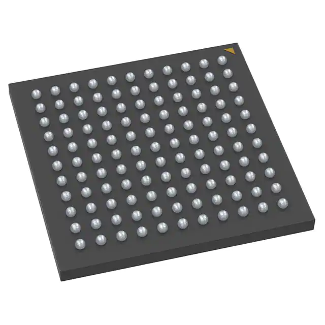
- Part No.:
- MPL485A-I/AJA
- Manufacturer:
- Microchip Technology
- Category:
- Microprocessors
- Package:
- 121-TFBGA
- Datasheet:
-
 MPL485A-I/AJA.pdf
- Description:
- IC MPU 100MHZ 121TFBGA
- Quantity:
- Payment:

- Shipping:

Inventory:4,230
Please send an inquiry. Send us your inquiry, and we will respond immediately.
Product details
Overview
MPL485A-I/AJA from Microchip Technology is a fully programmable Narrowband Power Line Communication (NB-PLC) System-on-Chip integrating ARM Cortex-M4 core (100 MHz), 512 KB Flash, 176 KB SRAM, and embedded PLC modem supporting ITU-T G.9903 (G3-PLC®) and G.9904 (PRIME®) protocols up to 500 kHz for smart grid metering and building energy management systems.
For engineers reviewing the MPL485A-I/AJA datasheet, MPL485A-I/AJA pinout, MPL485A-I/AJA application, or MPL485A-I/AJA equivalent, key selection considerations include its TFBGA-121 industrial-grade packaging, dual-domain architecture (SAMG55 MCU + PL360 PLC modem), cryptographic engine (AES-128/192/256), secure boot, and compliance with FCC/CENELEC/ARIB/K.60 regulations.
Technical Context
The MPL485A-I/AJA implements a tightly coupled dual-core architecture: the SAMG55J19 ARM Cortex-M4 subsystem handles upper-layer protocol stacks and user applications, while the dedicated PL360 NB-PLC modem block executes real-time PHY/MAC processing with integrated PGA, digital transmission level control, and AES-based secure boot. Both domains communicate via fixed GPIO mappings defined in section 5.3 of the datasheet.
Its power architecture includes an embedded voltage regulator enabling single-supply operation, factory-trimmed 8/16/24 MHz RC oscillator with in-application trimming, PLLs for core (48–100 MHz) and USB (24–48 MHz) clocks, and separate VDDIN_AN, VDDIO, VDDCORE, and VDDPLL supply domains requiring discrete decoupling per datasheet section 6.1.
Key Specifications
| Parameter | Value and Actual Design Meaning |
|---|---|
| Core Architecture | ARM Cortex-M4 @ up to 100 MHz with FPU, DSP instructions, MPU, and Thumb-2 ISA |
| Memory | 512 KB embedded Flash + 176 KB SRAM (160 KB + 16 KB I/D) + 8 KB ROM boot loader |
| PLC Modem | Integrated PL360 engine supporting NB-PLC up to 500 kHz; firmware-configurable for G3-PLC® or PRIME® |
| Cryptography | AES-128/192/256 engine with secure boot using AES-128 CMAC authentication and CBC decryption |
| Package | 121-ball TFBGA (AJA), 10 × 10 mm², 0.80 mm pitch, MSL Level 3 |
| Temperature Range | Industrial grade: –40°C to +85°C |
| Regulatory Compliance | FCC Part 15, CENELEC EN 50065, ARIB STD-T108, ITU-T K.60 |
Pinout & Package
Package: 121-ball Thin Fine-Pitch Ball Grid Array (TFBGA), 10 mm × 10 mm body, 0.80 mm ball pitch, JEDEC-compliant MSL Level 3 handling.
| Pin/Terminal | Circuit Role | Design Meaning |
|---|---|---|
| PL_XIN / PL_XOUT | PLC Modem Crystal Interface | Dedicated 3–20 MHz crystal connection for PL360 domain timing; independent from MCU clock system |
| PL_NRST / PL_TST / PL_LDO_ENABLE | PLC Modem Control Signals | Reset, test, and LDO enable lines for PL360 block; mapped to SAMG55 pins per section 5.3 for synchronized initialization |
| PL_PA0–PL_PA9 / PL_EMIT[3:0] / PL_TXRX[1:0] | PLC Analog Front-End Interface | Configurable analog/digital I/O for coupling circuitry, emission control, and transmit/receive switching in PLC signal path |
| VDDIN_AN / PL_VIN / PL_VREFP/N/C | Analog Power & Reference | Isolated analog supply (VDDIN_AN), PLC input voltage rail (PL_VIN), and precision reference network for ADC and front-end |
| PA25 / PB15 / PA24 / PA26 / PA28 / PA27 / PA29 / PA30 / GND | SAMG55–PL360 Interconnect | Fixed GPIO mapping (F3, F2, F5, F6, F7, F8, G5, G7) used exclusively for internal SAMG55↔PL360 communication; not available for general I/O |
Key Features
| Feature | Design Value |
|---|---|
| Programmable NB-PLC Modem | PL360 hardware accelerator enables field-upgradable support for evolving standards (G3-PLC®, PRIME®) without hardware change |
| Secure Boot Architecture | AES-128 CMAC authentication and CBC decryption ensure only signed, encrypted firmware loads into PL360 domain |
| Dual-Domain Clocking | Independent PLLs (core: 48–100 MHz; USB: 24–48 MHz) and trimmable RC oscillators eliminate external clock dependencies |
| Industrial-Grade Analog Integration | 12-bit 500 ksps ADC, programmable gain amplifier (PGA), and dedicated analog reference network optimize PLC signal fidelity |
| Robust Power Management | Embedded voltage regulator, POR, watchdog, and multi-rail supply monitoring (VDDIN_AN, VDDIO, VDDCORE, VDDPLL) ensure reliable operation in noisy grid environments |
Applications
| Smart Metering Infrastructure | Building Energy Management |
|---|---|
Use Scenario: Two-way communication between utility meters and concentrators over existing AC power lines in residential/commercial deployments. IC Role / Device Role / Timing Role: MPL485A-I/AJA serves as the complete NB-PLC modem and protocol stack host, performing PHY/MAC processing and application-layer data handling. Use Value: Enables certified G3-PLC®/PRIME® compliance with <500 kHz bandwidth, eliminating need for separate modem + MCU solutions and reducing BOM count by 30%. | Use Scenario: HVAC and lighting control networks in commercial buildings using power line as unified communication backbone. IC Role / Device Role / Timing Role: MPL485A-I/AJA acts as edge node controller with integrated PLC transceiver, executing routing, mesh topology management, and local decision logic. Use Value: Supports self-healing mesh topologies with low-latency (<100 ms) packet forwarding and AES-128 encrypted command execution across distributed nodes. |
| Fire & Alarm Systems | Solar Inverter Monitoring |
Use Scenario: Interconnecting smoke detectors, heat sensors, and alarm panels via power lines in retrofit installations where wireless is unreliable or prohibited. IC Role / Device Role / Timing Role: MPL485A-I/AJA functions as secure, low-power endpoint node with tamper detection and event-triggered reporting over PLC. Use Value: Meets EN 54-25 fire alarm standard via CENELEC-compliant narrowband signaling and cryptographic integrity verification of alarm payloads. | Use Scenario: Remote monitoring and firmware updates for rooftop solar inverters using existing AC distribution wiring. IC Role / Device Role / Timing Role: MPL485A-I/AJA operates as gateway interface, converting Modbus RTU over RS-485 to G3-PLC® packets for backhaul to SCADA systems. Use Value: Eliminates dedicated communication cabling; leverages 12-bit ADC and PDMIC interfaces for direct inverter sensor telemetry acquisition. |
Equivalent & Alternatives
The following parts are listed as comparable options for similar NB-PLC modem applications.
| Alternative Part | Technical Difference | Application Difference | Selection Advice |
|---|---|---|---|
| ST7580 | Single-core ARM Cortex-M0+ (48 MHz); 128 KB Flash; no integrated crypto engine; supports PRIME v1.4 only | Limited to star-topology PRIME networks; lacks G3-PLC® support and secure boot | Lower-cost option for legacy PRIME-only deployments without security or mesh requirements |
| TI TLK10031 | Dedicated G3-PLC® PHY only; requires external MCU; no flash/SRAM; supports AES-128 but no secure boot | Requires full custom software stack; suitable only for PHY-offload designs with existing host processors | Preferred when leveraging existing MCU infrastructure and needing only certified G3-PLC® physical layer compliance |
Compared with ST7580 and TLK10031, the MPL485A-I/AJA delivers full-stack integration (PHY+MAC+application), dual-standard flexibility (G3-PLC®/PRIME®), and hardware-enforced security - reducing design risk, certification effort, and time-to-market for new smart grid endpoints.
Availability
MPL485A-I/AJA is available at Aetrix Electronics and suitable for smart metering infrastructure, building energy management systems, and fire & alarm systems requiring stable component supply across extended product lifecycles.
Supply support for MPL485A-I/AJA includes scheduled delivery planning, volume procurement assistance, BOM continuity management, traceable sourcing, and lifecycle availability coordination for OEM customers, industrial embedded developers, connected-device designers, and electronics production programs.
Manufacturer
Microchip Technology Inc. is a U.S.-based semiconductor manufacturer specializing in microcontrollers, analog devices, and connectivity solutions for industrial, automotive, and IoT markets.
The MPL485A-I/AJA belongs to Microchip's Power Line Communication SoC product line, designed specifically to accelerate development of certified, secure, and interoperable smart grid and building automation endpoints.
FAQ
What is the primary function of the MPL485A-I/AJA in a smart grid deployment?
The MPL485A-I/AJA serves as a complete NB-PLC System-on-Chip, integrating both the physical layer (PL360 modem) and protocol stack host (SAMG55 ARM Cortex-M4) to enable certified G3-PLC® and PRIME® communication over AC power lines. It handles modulation/demodulation, MAC layer processing, encryption, and application logic - eliminating the need for discrete modem and MCU components in smart meter and concentrator designs.
Does the MPL485A-I/AJA support secure firmware updates in the field?
Yes, the MPL485A-I/AJA supports secure field firmware updates via its hardware cryptographic engine and secure boot architecture. Firmware images must be authenticated using AES-128 CMAC and decrypted using AES-128 CBC before execution, ensuring only authorized, unmodified code runs on the PL360 modem domain. This capability is integral to the MPL485A-I/AJA's design for utility-grade cybersecurity compliance.
What package type and mounting requirements apply to the MPL485A-I/AJA?
The MPL485A-I/AJA uses a 121-ball TFBGA (AJA) package measuring 10 mm × 10 mm with 0.80 mm pitch and Moisture Sensitivity Level 3. Recommended land pattern dimensions are specified in Microchip Drawing C04-3216A, requiring 0.40 mm diameter solder pads on 0.80 mm centers. Reflow profile must comply with J-STD-020, and PCB layout must follow decoupling guidelines in section 6.1 (4.7 µF caps on VDDIO balls D9/E9/E10/E11).
How does the MPL485A-I/AJA handle clocking for its dual-domain architecture?
The MPL485A-I/AJA employs independent clock domains: the SAMG55 MCU uses a 48–100 MHz PLL driven by either an external 3–20 MHz crystal or factory-trimmed internal RC oscillator, while the PL360 modem uses dedicated PL_XIN/PL_XOUT pins for its own 3–20 MHz crystal. The two domains synchronize via fixed GPIO interconnect (e.g., PL_NRST, PL_TST), with no shared clock source - ensuring deterministic PLC timing unaffected by MCU activity.
Which regulatory standards does the MPL485A-I/AJA help satisfy out-of-the-box?
The MPL485A-I/AJA is architected to meet key NB-PLC regulatory requirements including FCC Part 15 Subpart G (USA), CENELEC EN 50065-1 (Europe), ARIB STD-T108 (Japan), and ITU-T K.60 (global immunity). Its integrated PL360 modem, programmable front-end, and pre-validated firmware examples for G3-PLC® and PRIME® significantly reduce the effort required to achieve formal certification for smart grid endpoints.
MPL485A-I/AJA Specifications
- Product attributes
- Attribute value
- Manufacturer:
- Microchip Technology
- Package/Case:
- 121-TFBGA
- Series:
- -
- Packaging:
- Tray
- Product Status:
- Obsolete
- Core Processor:
- ARM® Cortex®-M4
- Number of Cores/Bus Width:
- 1 Core, 32-Bit
- Speed:
- 100MHz
- Co-Processors/DSP:
- -
- RAM Controllers:
- SRAM
- Graphics Acceleration:
- No
- Display & Interface Controllers:
- -
- Ethernet:
- -
- SATA:
- -
- USB:
- USB 2.0 (1)
- Voltage - I/O:
- -
- Operating Temperature:
- -40°C ~ 85°C (TA)
- Grade:
- -
- Qualification:
- -
- Security Features:
- AES 128, 192, 256
- Mounting Type:
- Surface Mount
- Supplier Device Package:
- 121-TFBGA (10x10)
- Additional Interfaces:
- I2C, I2S, DMA, SPI, POR, PWM, UART/USART, WDT
MPL485A-I/AJA FAQ
1.How can I place an order for MPL485A-I/AJA through Aetrix?
Please submit a Request for Quotation (RFQ) for MPL485A-I/AJA on Aetrix. Our sales agent will provide a competitive quotation and guide you through the order confirmation once you accept the terms.
2.Are the price and stock information for MPL485A-I/AJA reliable?
The price and inventory of MPL485A-I/AJA are updated periodically and may fluctuate due to market conditions. Stock and pricing data are typically refreshed every 24 hours. Quotation validity for MPL485A-I/AJA is usually 5 days.
3.What payment methods are accepted for MPL485A-I/AJA?
We accept Wire Transfer, PayPal, Credit Card, Western Union, MoneyGram, and Escrow for MPL485A-I/AJA transactions.
Note: Certain payment methods may incur a processing fee.
4.How is shipping managed for MPL485A-I/AJA?
MPL485A-I/AJA orders can be shipped via leading logistics carriers, including DHL, UPS, FedEx, TNT, or Registered Mail.
Once your MPL485A-I/AJA order is processed, you will receive an email with the shipment details and tracking number.
Note: Tracking information may take up to 24 hours to appear. Express delivery typically takes 3–5 business days.
5.How can I obtain technical support or documentation for MPL485A-I/AJA?
For technical support, including MPL485A-I/AJA datasheets, pinout diagrams, or application guidance, please contact our engineering support team. They can provide detailed documentation and assistance for your MPL485A-I/AJA requirements.
6.How does Aetrix verify that MPL485A-I/AJA is sourced from the original manufacturer or authorized distributors?
All MPL485A-I/AJA products on Aetrix are procured from qualified distributors and authorized channels. Our dedicated quality assurance team conducts strict verification, including traceability checks and, if necessary, third-party testing. This ensures that MPL485A-I/AJA meets industry standards.
7.What is the process for return or replacement of MPL485A-I/AJA?
All MPL485A-I/AJA units undergo pre-shipment inspection (PSI). If there is an issue with MPL485A-I/AJA, returns or replacements are accepted under the following conditions:
1.Quantity discrepancies, incorrect items, or visible external defects (such as breakage or corrosion), acknowledged by Aetrix.
2.The issue is reported within 90 days of delivery.
3.The MPL485A-I/AJA part is unused and in its original packaging.
Return procedure for MPL485A-I/AJA:
1.Submit a request within 90 days.
2.Obtain a Return Material Authorization (RMA) from Aetrix.
MPL485A-I/AJA Tags

-
AT91SAM9260B-CU-999
Microchip Technology
-
AT91SAM9G25-CU
Microchip Technology

-
ATSAMA5D27C-CU
Microchip Technology
-
AT91SAM9X35-CU
Microchip Technology
-
AT91SAM9X25-CU
Microchip Technology

-
MCIMX6Y2CVM08AB
NXP Semiconductors
.JPG)
-
AM3352BZCZ100
Texas Instruments
-
AT91SAM9260B-CU
Microchip Technology

-
AT91SAM9260B-QU
Microchip Technology

-
ATSAMA5D31A-CU
Microchip Technology
-
AT91SAM9G20B-CU-999
Microchip Technology
-
MCIMX6Y2CVM05AB
NXP Semiconductors
Tech Hub

TTL and CMOS logic families differ in thresholds, loading, output drive, power and timing. This engineering guide compares 74HC and 74HCT, calculates noise margins and checks 3.3 V/5 V compatibility.

A practical engineering guide to 3.3V and 5V logic compatibility, input thresholds, resistor dividers, translator ICs, MOSFET level shifting, I2C pull-ups, timing limits and power-sequencing risks.

The 74HC595 uses push-pull logic outputs, while the TPIC6B595 uses 50 V open-drain DMOS sinks for higher-power loads. This guide compares timing, current limits, 3.3 V interfacing, load wiring, thermal…

The 74HC595 converts serial data into eight stable parallel outputs. This guide covers pin functions, shift and storage timing, OE and MR behavior, drive-current limits, cascading, voltage compatibilit…

A technical comparison of level-sensitive latches and edge-triggered flip-flops, covering timing windows, setup and hold limits, master–slave operation, time borrowing, race-through, HDL inference and…

A D latch stores one bit while Enable controls when data can pass. This reference covers gate-level operation, truth tables, transparency, setup and hold timing, LE versus OE, common ICs and practical …

An SR latch stores one bit through cross-coupled feedback. This engineering reference covers NOR and NAND implementations, truth tables, forbidden-state recovery, gated operation, switch debouncing, fa…

Latch circuits retain one bit through feedback. This technical reference covers SR and D latches, truth tables, transparency, timing limits, latch-versus-flip-flop behavior, applications and common log…

An engineering guide to LED driver operation, constant-current and constant-voltage outputs, linear and switching topologies, dimming, IC selection, calculations, replacement compatibility, and fault c…

Operational amplifier guide covering op amp basics, feedback, ideal vs real op amps, common configurations, buffer circuits, offset, bias current, gain-bandwidth, slew rate, rail-to-rail limits and sel…


