
 My Inquiry
 My Account


Monolithic Power Systems Inc. MPM3593GQY-0001-T
- Part No.:
- MPM3593GQY-0001-T
- Manufacturer:
- Monolithic Power Systems Inc.
- Category:
- DC DC Converters
- Package:
- 41-PowerLQFN Module
- Datasheet:
-
 MPM3593GQY-0001-T.pdf
- Description:
- HIGH-EFFICIENCY, 45V, 3A, DIGITA
- Quantity:
- Payment:

- Shipping:

Inventory:4,684
Please send an inquiry. Send us your inquiry, and we will respond immediately.
Product details
Overview
MPM3593GQY-0001-T from Monolithic Power Systems is a digitally calibrated, synchronous step-down power module integrating high-side and low-side MOSFETs, I²C-configurable control, multi-page OTP memory, and full protection circuitry. It delivers up to 3A continuous output at ≤5V VOUT (2A at >5V), supports 3.5–45V input, and achieves 0.8–12V programmable output voltage with on-the-fly adjustment for industrial, automotive, and telecom DC/DC conversion.
For engineers reviewing the MPM3593GQY-0001-T datasheet, MPM3593GQY-0001-T pinout, MPM3593GQY-0001-T application, or MPM3593GQY-0001-T equivalent, this product enables rapid system-level optimization via I²C-adjusting switching frequency (250 kHz–2.5 MHz), soft-start time (0.5–4 ms), current limit (2–8 A), OVP thresholds, and thermal shutdown (125–175°C)-before permanently storing settings in OTP memory.
Technical Context
The MPM3593GQY-0001-T implements peak-current-mode PWM control with internal compensation, slope compensation, and configurable dead-time management. Its dual-mode operation-Advanced Asynchronous Modulation (AAM) for light-load efficiency and Forced Continuous Conduction Mode (FCCM) for low-noise fixed-frequency regulation-enables dynamic trade-off selection between efficiency and ripple performance.
It features an integrated 5V VCC LDO powered from VIN (or VOUT bias when enabled), configurable EN threshold (1.2–2 V), PG and /FT open-drain fault indicators, SYNCIN/SYNCO capability, and I²C-address setting via external resistor. All register-based parameters-including UVLO, OVP, soft-start slew rate (1–4 V/ns), and valley/peak current limits-are validated across –40°C to +150°C junction temperature.
Key Specifications
| Parameter | Value and Actual Design Meaning |
|---|---|
| VIN Range | 3.5V to 45V - supports wide-input industrial and automotive battery rails without pre-regulation. |
| IOUT Capability | 3A continuous at VOUT ≤ 5V; 2A at VOUT > 5V - defined by thermal derating and internal FET RDS(ON) (HS: 95–180 mΩ, LS: 50–100 mΩ). |
| VOUT Programmability | 0.8V–12V (VIN ≤ 24V); 0.8V–8V (VIN > 24V) - adjusted in real time via I²C, enabling single-BOM flexibility across multiple output voltages. |
| fSW Range | 250 kHz to 2.5 MHz - configurable for EMI reduction (via dithering), layout optimization, or efficiency tuning. |
| Protection Features | UVLO (2.9–3.4 V), OVP (110–130% of VOUT), OCP (2–8 A peak), over-temperature shutdown (125–175°C) - all user-configurable thresholds stored in OTP. |
| Soft-Start Time | 0.5 ms to 4 ms - adjustable via I²C register to prevent inrush current during power-up sequencing. |
| Thermal Resistance | θJA = 26°C/W (EVM3593-QY-00B, 4-layer PCB) - enables 3A operation at TA ≤ 85°C with standard copper pour. |
Pinout & Package
MPM3593GQY-0001-T is housed in a thermally enhanced QFN-41 package (6 mm × 8 mm, 0.5 mm pitch) with exposed thermal pad (PGND-connected) for efficient heat dissipation in high-power density applications.
| Pin/Terminal | Circuit Role | Design Meaning |
|---|---|---|
| 1,2,3,4,36 | VOUT | Main regulated output node - connects directly to output capacitor bank and load; multiple pins reduce IR drop and improve current sharing. |
| 5,6 | BST | Bootstrap supply for HS-FET gate driver - requires internal 0.1 µF BST–SW capacitor; floating-capable for layout flexibility. |
| 7 | VCC | Internal 5V LDO output - powers logic and analog blocks; decoupled by internal 1 µF capacitor; supports VOUT bias mode when VOUT > 5V. |
| 8 | AGND | Signal ground reference - isolated from PGND internally; must be connected to power ground on PCB for noise immunity and accurate feedback sensing. |
| 9 | VOUT_S | Precision output voltage sense - enables remote sensing for improved load regulation; bypasses internal FB divider when used. |
| 10 | ADD | I²C address configuration - sets device address via external resistor to avoid bus conflicts in multi-module systems. |
| 11,12 | SYNC | Configurable sync interface - selectable as SYNCIN (for clock synchronization) or SYNCO (for master clock output) via I²C register. |
| 13–15,39 | VIN | Main input supply - multiple pins minimize trace inductance and reduce switching noise coupling into sensitive circuits. |
| 16–18,40 | PGND | Power ground return - tied to thermal pad; must connect to large copper area for thermal management and low-impedance return path. |
| 19,20 | EN | Enable control input - active-high digital enable; threshold configurable from 1.2 V to 2 V; must not be floated. |
| 21 | PG | Open-drain power-good indicator - asserts after VOUT reaches 86–92% of target and remains stable for ≥30 µs; used for system sequencing. |
| 22 | /FT | Open-drain fault indicator - pulled low on OVP, OCP, UVLO, or thermal shutdown; provides immediate system-level fault signaling. |
| 23 | SCL | I²C serial clock input - supports standard-mode (400 kHz) timing; rise/fall times specified for 400 pF bus capacitance. |
| 24 | SDA | I²C bidirectional data line - supports read/write access to all configuration registers and status flags. |
| 25,26,41 | SW | Switch node - internally connected to integrated inductor; high dv/dt node requiring tight layout and minimal loop area. |
| 27,35,38 | NC | No-connect - must remain unconnected and un-bonded on PCB; floating per datasheet requirement. |
Key Features
| Feature | Design Value |
|---|---|
| Digitally calibrated OTP storage | Multi-page one-time programmable memory retains I²C-configured settings (VOUT, fSW, OVP, soft-start, etc.) after power cycle - eliminates external EEPROM or firmware dependency. |
| Configurable light-load efficiency | AAM mode reduces quiescent current to ~1 µA in sleep state while maintaining fast wake-up; FCCM option preserves fixed-frequency operation for noise-sensitive loads. |
| Low-EMI design support | Frequency dithering, adjustable slew rate (1–4 V/ns), and SYNC capability enable compliance with CISPR 22/EN55022 Class B conducted/radiated emissions limits. |
| Integrated thermal and fault management | Programmable thermal shutdown (125–175°C) with 25–50°C hysteresis, plus independent OVP/OCP/UVLO thresholds - allows precise margining for safety-critical systems. |
| Flexible feedback architecture | Supports both internal FB divider (0.8–12V) and external resistor network with VOUT_S sense - enables precision regulation and compatibility with legacy designs. |
Applications
| Industrial PLC Power Supply | Automotive ADAS Camera Module |
|---|---|
|
Use Scenario: Provides stable 5V/3A rail for FPGA, image sensor, and ISP in programmable logic controllers operating from 24V DC field buses. IC Role / Device Role / Timing Role: Primary synchronous buck regulator with I²C-configurable soft-start and OVP to meet IEC 61000-4-5 surge immunity requirements. Use Value: OTP-stored settings ensure repeatable startup behavior across production units; PG and /FT signals enable deterministic system-level fault recovery. |
Use Scenario: Generates 3.3V/3A for CMOS image sensors and SerDes links in rear-view and surround-view camera ECUs powered from 12V vehicle battery. IC Role / Device Role / Timing Role: Digitally tunable DC/DC converter supporting AEC-Q100 Grade 1 temperature range (–40°C to +125°C) with fast transient response (<100 µs). Use Value: Configurable switching frequency avoids AM radio band interference; SYNC input aligns switching edges across multiple cameras to suppress beat frequencies. |
| Telecom Base Station RF Front-End | Medical Imaging Sensor Interface |
|
Use Scenario: Supplies clean 12V/2A bias to GaN power amplifiers and low-noise amplifiers in small-cell base stations with 48V PoE-derived input. IC Role / Device Role / Timing Role: High-efficiency, low-ripple synchronous buck with FCCM mode selected to minimize switching noise near sensitive RF receivers. Use Value: Adjustable slew rate and frequency dithering reduce conducted EMI; VOUT_S sensing ensures ±0.5% regulation under dynamic RF load modulation. |
Use Scenario: Powers high-resolution analog front-end (AFE) and ADC in portable ultrasound probes using 24V medical-grade input. IC Role / Device Role / Timing Role: Precision-regulated, low-noise power source with programmable OVP (115–125% of VOUT) and thermal monitoring for patient-safety compliance. Use Value: Multi-threshold fault reporting (/FT + PG) enables redundant health monitoring; OTP storage guarantees consistent calibration across probe lifetime. |
Equivalent & Alternatives
The following parts are listed as comparable options for similar digitally configurable synchronous step-down module applications.
| Alternative Part | Technical Difference | Application Difference | Selection Advice |
|---|---|---|---|
| MPM3695GQY-0001-T | Higher 6A rating, 60V max VIN, dual-phase support, but no OTP memory - requires external MCU for configuration persistence. | Targeted at higher-power server/industrial applications where OTP is less critical than current capacity. | Select when >3A output or >45V input is required; accept added firmware complexity for non-volatile configuration. |
| TPS546D24RVFT | PMBus interface (not I²C), 40V max VIN, 10A output, integrated telemetry (V/I/T), but larger 7mm × 7mm QFN-53 package. | Used in datacenter VRMs where PMBus telemetry and higher current dominate over compact size and OTP simplicity. | Choose when real-time telemetry and PMBus ecosystem integration outweigh I²C convenience and OTP retention. |
Compared with MPM3593GQY-0001-T, the MPM3695GQY-0001-T trades OTP simplicity for higher current and voltage headroom, while the TPS546D24RVFT replaces I²C configurability with PMBus telemetry and broader industry tooling support-making each suitable for distinct system-level priorities.
Availability
MPM3593GQY-0001-T is available at Aetrix Electronics and suitable for industrial PLC power supplies, automotive ADAS camera modules, telecom RF front-ends, and medical imaging sensor interfaces requiring stable component supply, long-term lifecycle assurance, and qualified automotive-grade variants.
Supply support for MPM3593GQY-0001-T includes scheduled delivery planning, volume procurement assistance, BOM continuity management, traceable sourcing, and lifecycle availability coordination for OEM customers, industrial embedded developers, connected-device designers, and electronics production programs.
Manufacturer
Monolithic Power Systems (MPS) is a fabless semiconductor company specializing in high-performance power management ICs and modules, with over two decades of innovation in DC/DC conversion, motor drivers, and LED lighting solutions.
The MPM3593 belongs to MPS's digitally programmable power module product line, designed specifically for applications demanding rapid configuration, field-upgradable settings, and robust protection in space-constrained industrial and automotive environments.
FAQ
What is the default output voltage and how is it set?
The MPM3593GQY-0001-T defaults to 5.0 V ±0.075 V (–40°C to +125°C) via internal factory-programmed OTP registers. This value is established during final test and cannot be altered without reprogramming OTP - which is irreversible. The default is confirmed by register 00h bits[7:0] = 0x64 and 01h bits[1:0] = 0b01 in the datasheet.
Can the I²C interface be used after power-up without enabling EN?
No. The I²C interface is disabled until the EN pin voltage exceeds 2 V, at which point the internal logic and I²C block are powered and accessible. Below 2 V, the I²C bus is blocked and all RAM registers reset to their OTP-stored defaults - ensuring deterministic behavior during brown-out or partial power conditions.
How does the VOUT_S pin affect regulation accuracy?
VOUT_S enables remote sensing by connecting directly to the load point, bypassing PCB trace resistance. When enabled, it overrides the internal FB divider and improves load regulation to ±0.1% (vs. ±0.3% with internal sensing), critical for high-precision analog or high-current digital loads where trace IR drop exceeds 10 mV.
Is the QFN-41 thermal pad electrically connected to PGND?
Yes. The exposed thermal pad on the QFN-41 package is internally bonded to PGND and must be soldered to a dedicated PGND copper pour on the PCB. This connection serves both thermal conduction (reducing θJA by ~10°C/W) and electrical grounding for the power stage - failure to connect degrades efficiency and may trigger thermal shutdown prematurely.
What happens during thermal shutdown and how is recovery managed?
When junction temperature reaches the programmed TSD threshold (default 175°C), the device halts switching, pulls /FT low, and holds PG low. Recovery occurs only after temperature falls below TSD minus hysteresis (default 25°C), at which point soft-start reinitiates. No external reset is needed - the behavior is fully autonomous and documented in register 07h bits[7:6] and bit[5].
Does the MPM3593GQY-0001-T support spread-spectrum frequency modulation?
No. It supports frequency dithering - a deterministic, bounded variation of fSW (±5–10% around center frequency) controlled via I²C register 03h bits[5:4] - which reduces peak EMI amplitude without introducing jitter into timing-critical systems. True spread-spectrum (SSFM) with random modulation is not implemented.
Can multiple MPM3593GQY-0001-T devices share the same I²C bus?
Yes, provided each device has a unique I²C address set via the ADD pin resistor. Up to eight devices can coexist on one bus (7-bit addressing, 0x60–0x67 range). Synchronization is also possible: one unit can drive SYNC as master (SYNCO), while others configure SYNC as slave (SYNCIN) to align switching edges and minimize beat frequencies.
MPM3593GQY-0001-T Specifications
- Product attributes
- Attribute value
- Manufacturer:
- Monolithic Power Systems Inc.
- Series:
- MPM
- Package/Case:
- 41-PowerLQFN Module
- Packaging:
- Bulk
- Product Status:
- Active
- Type:
- Non-Isolated PoL Module, Digital
- Number of Outputs:
- 1
- Voltage - Input (Min):
- 3.5V
- Voltage - Input (Max):
- 45V
- Voltage - Output 1:
- 0.8 ~ 12V
- Voltage - Output 2:
- -
- Voltage - Output 3:
- -
- Voltage - Output 4:
- -
- Current - Output (Max):
- 3A
- Power (Watts):
- 36 W
- Voltage - Isolation:
- -
- Applications:
- ITE (Commercial)
- Features:
- Adjustable Output, I2C Interface
- Operating Temperature:
- -40°C ~ 150°C (With Derating)
- Efficiency:
- -
- Grade:
- -
- Qualification:
- -
- Mounting Type:
- Surface Mount
- Supplier Device Package:
- 41-QFN (6x8)
- Control Features:
- -
- Approval Agency:
- -
- Standard Number:
- -
MPM3593GQY-0001-T FAQ
1.How can I place an order for MPM3593GQY-0001-T through Aetrix?
Please submit a Request for Quotation (RFQ) for MPM3593GQY-0001-T on Aetrix. Our sales agent will provide a competitive quotation and guide you through the order confirmation once you accept the terms.
2.Are the price and stock information for MPM3593GQY-0001-T reliable?
The price and inventory of MPM3593GQY-0001-T are updated periodically and may fluctuate due to market conditions. Stock and pricing data are typically refreshed every 24 hours. Quotation validity for MPM3593GQY-0001-T is usually 5 days.
3.What payment methods are accepted for MPM3593GQY-0001-T?
We accept Wire Transfer, PayPal, Credit Card, Western Union, MoneyGram, and Escrow for MPM3593GQY-0001-T transactions.
Note: Certain payment methods may incur a processing fee.
4.How is shipping managed for MPM3593GQY-0001-T?
MPM3593GQY-0001-T orders can be shipped via leading logistics carriers, including DHL, UPS, FedEx, TNT, or Registered Mail.
Once your MPM3593GQY-0001-T order is processed, you will receive an email with the shipment details and tracking number.
Note: Tracking information may take up to 24 hours to appear. Express delivery typically takes 3–5 business days.
5.How can I obtain technical support or documentation for MPM3593GQY-0001-T?
For technical support, including MPM3593GQY-0001-T datasheets, pinout diagrams, or application guidance, please contact our engineering support team. They can provide detailed documentation and assistance for your MPM3593GQY-0001-T requirements.
6.How does Aetrix verify that MPM3593GQY-0001-T is sourced from the original manufacturer or authorized distributors?
All MPM3593GQY-0001-T products on Aetrix are procured from qualified distributors and authorized channels. Our dedicated quality assurance team conducts strict verification, including traceability checks and, if necessary, third-party testing. This ensures that MPM3593GQY-0001-T meets industry standards.
7.What is the process for return or replacement of MPM3593GQY-0001-T?
All MPM3593GQY-0001-T units undergo pre-shipment inspection (PSI). If there is an issue with MPM3593GQY-0001-T, returns or replacements are accepted under the following conditions:
1.Quantity discrepancies, incorrect items, or visible external defects (such as breakage or corrosion), acknowledged by Aetrix.
2.The issue is reported within 90 days of delivery.
3.The MPM3593GQY-0001-T part is unused and in its original packaging.
Return procedure for MPM3593GQY-0001-T:
1.Submit a request within 90 days.
2.Obtain a Return Material Authorization (RMA) from Aetrix.
MPM3593GQY-0001-T Tags
-
1S4E_0505S1.5U
GAPTEC Electronic
-
TPS631000DRLR
Texas Instruments
-
XCL209F083DR
Torex Semiconductor Ltd
-
SC202AMLTRT
Semtech Corporation

-
NME1S0505SC
Murata Power Solutions Inc.
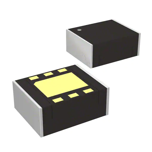
-
XCL101A501ER-G
Torex Semiconductor Ltd
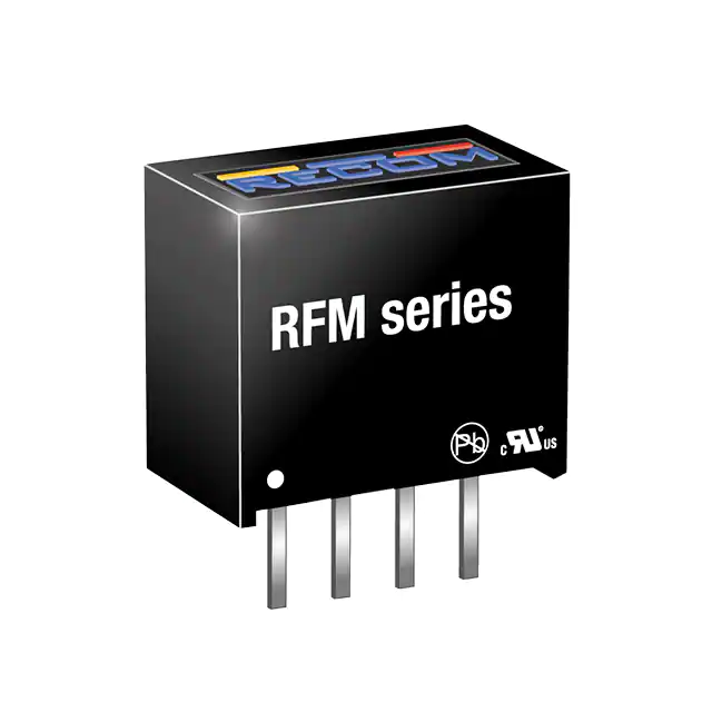
-
RFM-0505S
Recom Power
-
TEA 1-0505E
Traco Power
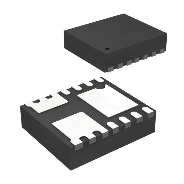
-
MIC33153YHJ-TR
Microchip Technology
-
TEA 1-0505
Traco Power
-
TPSM863252RDXR
Texas Instruments
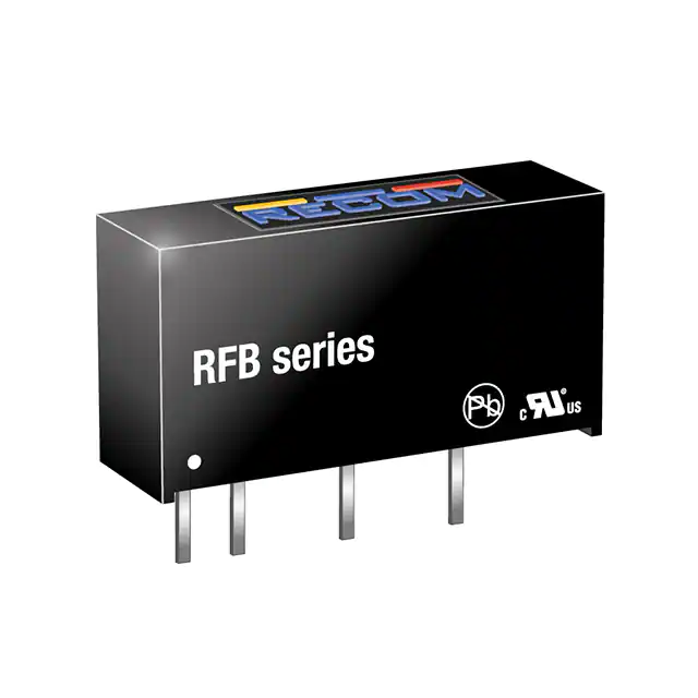
-
RFB-0505S
Recom Power
Tech Hub

Operational amplifier guide covering op amp basics, feedback, ideal vs real op amps, common configurations, buffer circuits, offset, bias current, gain-bandwidth, slew rate, rail-to-rail limits and sel…

Jumper cables guide covering safe connection order, red and black clamp placement, final ground connection, cable gauge, length, clamp quality, copper vs CCA cables, jump starter comparison and battery…

LDO regulator guide covering low dropout voltage, power dissipation, thermal design, PSRR, output noise, capacitor stability, adjustable LDO circuits, LDO vs buck converter and datasheet selection chec…

Conditional Access Module guide covering CAM meaning, CI/CI+ interface, smart card authorization, DVB security workflow, TV and set-top box compatibility, internal electronics, ESD protection, connecto…

Guide to electronic component obsolescence covering EOL risk, PCN/PDN notices, last-time buy planning, replacement options, form-fit-function validation, counterfeit risk and BOM lifecycle management.

18650 battery guide covering lithium-ion cell basics, 3.6V/3.7V voltage, 4.2V charging, mAh and Wh capacity, protected cells, chargers, BMS, series-parallel packs, holders, welding and sourcing checks.…

Hall effect sensor guide covering working principle, linear and digital sensors, Arduino circuits, current sensing, speed detection, automotive applications, A3144 examples, signal filtering and datash…

Product Change Notification guide for electronic components, covering PCN meaning, PCN vs PDN/EOL, common change types, risk levels, form-fit-function review, engineering validation, BOM control, LTB/L…

A practical guide to blend door actuators, covering HVAC function, symptoms, location, AC and heater issues, reset and calibration, replacement cost, electrical diagnosis, compatibility checks, and rep…

Engineering guide to Raspberry Pi alternatives, covering chip-level differences, Orange Pi, ROCK, Jetson, Banana Pi, NanoPi, Compute Module, Pico, GPIO, camera, HAT compatibility, and replacement risks…


