
 My Inquiry
 My Account


Monolithic Power Systems Inc. MPQ5480GC-Z
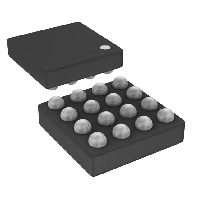
- Part No.:
- MPQ5480GC-Z
- Manufacturer:
- Monolithic Power Systems Inc.
- Category:
- Battery Chargers
- Package:
- 16-UFBGA, WLCSP
- Datasheet:
-
 MPQ5480GC-Z.pdf
- Description:
- IC BATT CHG LI-ION 16WLCSP
- Quantity:
- Payment:

- Shipping:

Inventory:2,902
Please send an inquiry. Send us your inquiry, and we will respond immediately.
Product details
Overview
MPQ5480GC-Z from Monolithic Power Systems is a monolithic power management IC for wearable devices, integrating a USB-compatible constant-current/constant-voltage lithium-ion battery charger, a synchronous step-down DC/DC regulator (1.22V default, 100mA output), cell under-voltage protection, and a system extension switch (Vo2). It operates with 4V–6V charger input, supports push-button enable/disable control, and delivers stable regulation in WLCSP-16 (1.7mm×1.7mm) packaging.
For engineers reviewing the MPQ5480GC-Z datasheet, MPQ5480GC-Z pinout, MPQ5480GC-Z application, or MPQ5480GC-Z equivalent, this device serves as a compact, low-quiescent-power solution for space-constrained battery-powered systems requiring integrated charge management, regulated rail generation, and controlled power distribution - especially where thermal shutdown, cycle-by-cycle current limiting, and dead-battery detection are critical.
Technical Context
The MPQ5480GC-Z implements a hysteresis-controlled synchronous buck converter with programmable peak current limit (via IPK pin resistor), internal 2kΩ series resistance, and DCM/CCM hybrid operation for fast transient response and minimal output capacitance. Its CC/CV charger uses external RICHG to set charge current (7.8–127mA), includes trickle-charge mode below 2.93V, and enforces thermal limits (6°C–49°C) before charging initiation.
System-level control integrates a 2.2s debounce timer and toggle flip-flop on EN/PB, latching shutdown when VBATT < 3.05V (UVLO), disabling DC/DC and Vo2 during charging (VCH > 3.8V), and enabling auto-retry protection on Vo2 with 9ms overcurrent and 300µs short-circuit detection delays.
Key Specifications
| Parameter | Value and Actual Design Meaning |
|---|---|
| Charger Input Range | 4V to 6V - USB-compliant range ensuring compatibility with standard 5V sources while tolerating cable drop. |
| DC/DC Output Current | 100mA - Maximum continuous load supported by internal synchronous FETs without thermal derating at TA = +25°C. |
| Default VOUT Accuracy | ±1% at 1.22V - Tight regulation enables precision biasing of low-power sensors or microcontrollers. |
| Feedback Voltage | 1.22V - Internal reference used with external resistor divider to scale output up to ≥1.22V. |
| Peak Inductor Current | 100mA (RIPK = 17.8kΩ) - Programmable limit protects battery and inductor during startup and transients. |
| Quiescent Current (BATT) | 40–55μA - Ultra-low operating IQ extends runtime in always-on wearable standby modes. |
| UVLO Threshold | 3.05V ±60mV - Prevents system operation below safe Li-ion discharge voltage, avoiding cell damage. |
Pinout & Package
MPQ5480GC-Z is housed in a WLCSP-16 package (1.7mm × 1.7mm, 0.4mm pitch), optimized for ultra-compact wearable PCB layouts with bottom-soldered ball grid array.
| Pin/Terminal | Circuit Role | Design Meaning |
|---|---|---|
| A1 CH | Charger input | Accepts 4–6V USB-compatible source; enables CC/CV charging and disables DC/DC when active. |
| A2 ICHG | Charge current set | Connects to ground via resistor to program ICHG (7.8–127mA); sets full-charge termination threshold. |
| B1 BATT | Battery connection | Direct interface to single-cell Li-ion; feeds UVLO sensing (EOL), charger, and DC/DC input. |
| B2 Vo2 | System extension switch | Controlled high-side switch delivering VBATT to auxiliary circuitry; includes OCP/SCP with 75ms auto-retry. |
| B4 EN/PB | Push-button enable | Toggle input with 2.2s debounce; controls DC/DC and Vo2 ON/OFF state when no charger is present. |
| C1 PGND | Power ground | High-current return path for charger, DC/DC switch node (SW), and Vo2 FET; requires low-impedance layout. |
| C2 AGND | Analog ground | Reference for feedback comparators, UVLO, and current sense; must be separated from PGND and tied at single point. |
| D1 SW | DC/DC switch node | Drives external 10µH inductor; connects to internal HS/LS FETs; requires tight loop with CIN and COUT. |
| D2 VOUT | DC/DC regulated output | Delivers 1.22V (±1%) or programmable voltage; supplies core logic rails; stable with ceramic capacitors ≥10µF. |
| D3 IPK | Peak current set | Resistor-to-ground sets inductor peak current (30–200mA); internal 2kΩ resistor prevents runaway at RIPK = 0. |
Key Features
| Feature | Design Value |
|---|---|
| Hysteresis-controlled buck topology | Eliminates need for external compensation; achieves fast load transient response (<100µs) and inherent loop stability. |
| Integrated push-button debouncer | 2.2s hardware debounce with idle-mode power gating reduces system MCU wake-up burden and false triggers. |
| Cell protection suite | Includes UVLO (3.05V), thermal cutoff (125°C junction), cycle-by-cycle current limiting, and short-circuit shutdown. |
| Programmable dual-rail control | VOUT set via resistor divider; Vo2 provides independent battery-switched rail with OCP/SCP and auto-retry recovery. |
| Low-ESR ceramic capacitor support | Stable operation with ≥10µF X5R/X7R ceramics eliminates electrolytic bulk caps, saving board area and improving reliability. |
Applications
| Smart Fitness Tracker | Wireless Earbud Charging Case |
|---|---|
|
Use Scenario: Compact enclosure housing rechargeable Li-ion battery, BLE SoC, and motion sensor, requiring multi-rail power sequencing and long shelf life. IC Role / Device Role / Timing Role: Single-chip PMIC managing battery charge (CC/CV), generating 1.22V rail for sensor bias, and enabling/disabling earbud charging circuit via Vo2. Use Value: Reduces BOM count by replacing discrete charger + LDO + load switch; 40μA quiescent current extends case standby time beyond 6 months. |
Use Scenario: Dual-battery compartment charging case with status LED, USB-C input, and individual earbud charging control. IC Role / Device Role / Timing Role: Charger regulates main case battery; Vo2 switch gates power to earbud charging circuit only when case battery >3.05V and push-button is active. Use Value: Prevents parasitic drain during storage; Vo2's 3.8×ICHG overcurrent threshold avoids false trips during earbud insertion surge. |
| Medical Patch Monitor | AR Glasses Control Module |
|
Use Scenario: Disposable skin-adhered ECG patch with 30-day operational life, requiring precise low-noise analog supply and battery health monitoring. IC Role / Device Role / Timing Role: Provides 1.22V ±1% analog rail for ADC reference and op-amps; EOL pin monitors filtered battery voltage for predictive end-of-life alerts. Use Value: Tight VOUT accuracy ensures <0.5% measurement error drift; UVLO hysteresis-free latch prevents erratic restarts near depletion. |
Use Scenario: Head-mounted display subsystem with IMU, microdisplay driver, and Bluetooth module, powered by embedded Li-ion cell. IC Role / Device Role / Timing Role: Synchronous buck delivers clean 1.22V rail to display timing controller; EN/PB enables full-system power-on only after user press confirms intent. Use Value: 0.3ms soft-start suppresses inrush into display capacitors; DCM operation minimizes audible noise during low-brightness UI states. |
Equivalent & Alternatives
The following parts are listed as comparable options for similar integrated charger + buck regulator applications.
| Alternative Part | Technical Difference | Application Difference | Selection Advice |
|---|---|---|---|
| MPS MPQ5472GC-Z | Higher DC/DC output (300mA), no Vo2 switch, no push-button controller, same WLCSP-16 package. | Suitable for higher-power wearables needing only charge + regulation, not system extension or tactile enable. | Select when load exceeds 100mA and Vo2/EN/PB features are unnecessary - trades integration for higher current capability. |
| Texas Instruments BQ24075RGTR | Standalone linear charger (no integrated DC/DC), 1.5A max charge current, 20-pin QFN, no Vo2 or buck regulator. | Requires external LDO/buck for system rail; better for cost-sensitive designs where regulation is handled separately. | Choose when charger performance (1.5A) is primary need and board space allows separate DC/DC; lacks MPQ5480GC-Z's system-level integration. |
Compared with MPQ5472GC-Z, MPQ5480GC-Z trades 200mA DC/DC headroom for essential system-control functions (Vo2, EN/PB, dead-battery detection); versus BQ24075RGTR, it eliminates two ICs but constrains charge current to 127mA max - making it optimal for sub-100mA wearable subsystems demanding minimal footprint and autonomous power sequencing.
Availability
MPQ5480GC-Z is available at Aetrix Electronics and suitable for wearable device design, medical patch monitors, wireless earbud charging cases, and AR glasses control modules requiring stable component supply across prototyping, NPI, and volume production phases.
Supply support for MPQ5480GC-Z includes scheduled delivery planning, volume procurement assistance, BOM continuity management, traceable sourcing, and lifecycle availability coordination for OEM customers, industrial embedded developers, connected-device designers, and electronics production programs.
Manufacturer
Monolithic Power Systems (MPS) is a fabless semiconductor company specializing in high-performance analog and power ICs, with emphasis on efficiency, miniaturization, and reliability for portable and industrial applications.
The MPQ5480 belongs to MPS's wearable-optimized PMIC product line, designed specifically to consolidate charging, regulation, protection, and user-interface control into a single WLCSP die for sub-20mm² end equipment.
FAQ
What is the maximum charge current supported by MPQ5480GC-Z?
The MPQ5480GC-Z supports a maximum programmed charge current of 127mA, achieved when the ICHG pin is shorted to ground (RICHG = 0kΩ). This value is confirmed in the Electrical Characteristics table (page 4) under "Constant current regulation" with ICHG = 127mA at RICHG = 0kΩ. Higher currents require external charge ICs.
Can MPQ5480GC-Z regulate output voltages above 1.22V?
Yes - the default 1.22V output is programmable using an external resistor divider from VOUT to AGND. The datasheet (page 14) provides the formula VO = [1 + RUP/(RDOWN // 900kΩ)] × 1.22V, where 900kΩ is the internal FB divider sum. This allows precise scaling to common rails like 1.8V or 3.3V with appropriate resistor selection.
How does the Vo2 switch behave during charging?
When a valid charger is connected (VCH > 3.8V), the Vo2 switch is forcibly disabled regardless of EN/PB state - as stated in the Operation section (page 13): "The output of the flip-flop is forced to low when VCH is connected… it forces the DC/DC and Vo2 MOSFET to be disabled." This prevents backfeed and ensures charger priority.
Is MPQ5480GC-Z still in active production?
No - the datasheet header explicitly labels MPQ5480 as "END OF LIFE" (page 1). While Aetrix Electronics maintains legacy inventory and offers lifecycle coordination support, new designs should consider migration paths such as the MPQ5472GC-Z or consult MPS for qualified replacements per their PCN notifications.
What is the purpose of the capacitor on the EOL pin?
A 0.1µF capacitor on the EOL pin creates a 1ms RC low-pass filter for battery voltage, providing averaged VBATT sampling to the UVLO comparator. As described on page 12, this filtering prevents false shutdowns due to transient dips during pulsed loads, ensuring reliable latched shutdown only when true under-voltage persists.
Does MPQ5480GC-Z support automatic recharging after battery recovery?
No - once latched in shutdown (VBATT < Vth_UVLO), the device remains off until an external charger is applied to the CH pin (VCH > 3.8V), as stated on page 12: "MPQ5480 is latched in this shutdown mode until a valid external power source is connected to CH pin." No autonomous wake-up occurs upon battery voltage rise alone.
What inductor value is recommended for MPQ5480GC-Z's DC/DC section?
The datasheet specifies a 10µH inductor in all test conditions (pages 4–5, 14) and recommends it to maintain switching frequency above 20kHz under light load - preventing audible noise. The inductor must handle ≥100mA peak current and exhibit low DCR to preserve efficiency; shielded types (e.g., TDK VLS201610) are preferred for EMI control.
MPQ5480GC-Z Specifications
- Product attributes
- Attribute value
- Manufacturer:
- Monolithic Power Systems Inc.
- Series:
- -
- Package/Case:
- 16-UFBGA, WLCSP
- Packaging:
- Tape & Reel (TR)
- Product Status:
- Active
- Battery Chemistry:
- Lithium Ion
- Number of Cells:
- -
- Current - Charging:
- Constant
- Programmable Features:
- Voltage
- Fault Protection:
- Over Current, Over Temperature, Short Circuit
- Charge Current - Max:
- 100mA
- Battery Pack Voltage:
- 4.1V
- Voltage - Supply (Max):
- 6V
- Interface:
- USB
- Operating Temperature:
- -40°C ~ 125°C (TJ)
- Grade:
- -
- Qualification:
- -
- Mounting Type:
- Surface Mount
- Supplier Device Package:
- 16-WLCSP (1.7x1.7)
MPQ5480GC-Z FAQ
1.How can I place an order for MPQ5480GC-Z through Aetrix?
Please submit a Request for Quotation (RFQ) for MPQ5480GC-Z on Aetrix. Our sales agent will provide a competitive quotation and guide you through the order confirmation once you accept the terms.
2.Are the price and stock information for MPQ5480GC-Z reliable?
The price and inventory of MPQ5480GC-Z are updated periodically and may fluctuate due to market conditions. Stock and pricing data are typically refreshed every 24 hours. Quotation validity for MPQ5480GC-Z is usually 5 days.
3.What payment methods are accepted for MPQ5480GC-Z?
We accept Wire Transfer, PayPal, Credit Card, Western Union, MoneyGram, and Escrow for MPQ5480GC-Z transactions.
Note: Certain payment methods may incur a processing fee.
4.How is shipping managed for MPQ5480GC-Z?
MPQ5480GC-Z orders can be shipped via leading logistics carriers, including DHL, UPS, FedEx, TNT, or Registered Mail.
Once your MPQ5480GC-Z order is processed, you will receive an email with the shipment details and tracking number.
Note: Tracking information may take up to 24 hours to appear. Express delivery typically takes 3–5 business days.
5.How can I obtain technical support or documentation for MPQ5480GC-Z?
For technical support, including MPQ5480GC-Z datasheets, pinout diagrams, or application guidance, please contact our engineering support team. They can provide detailed documentation and assistance for your MPQ5480GC-Z requirements.
6.How does Aetrix verify that MPQ5480GC-Z is sourced from the original manufacturer or authorized distributors?
All MPQ5480GC-Z products on Aetrix are procured from qualified distributors and authorized channels. Our dedicated quality assurance team conducts strict verification, including traceability checks and, if necessary, third-party testing. This ensures that MPQ5480GC-Z meets industry standards.
7.What is the process for return or replacement of MPQ5480GC-Z?
All MPQ5480GC-Z units undergo pre-shipment inspection (PSI). If there is an issue with MPQ5480GC-Z, returns or replacements are accepted under the following conditions:
1.Quantity discrepancies, incorrect items, or visible external defects (such as breakage or corrosion), acknowledged by Aetrix.
2.The issue is reported within 90 days of delivery.
3.The MPQ5480GC-Z part is unused and in its original packaging.
Return procedure for MPQ5480GC-Z:
1.Submit a request within 90 days.
2.Obtain a Return Material Authorization (RMA) from Aetrix.
MPQ5480GC-Z Tags

-
BQ21040DBVR
Texas Instruments

-
MCP73812T-420I/OT
Microchip Technology
-
MCP73831T-2ACI/OT
Microchip Technology
-
MCP73832T-2ACI/OT
Microchip Technology
-
MCP73831T-2DCI/OT
Microchip Technology
-
MCP73832T-2DCI/OT
Microchip Technology
-
MCP73831T-2ATI/OT
Microchip Technology
-
MCP73832T-2ATI/OT
Microchip Technology
-
MCP73831T-5ACI/OT
Microchip Technology

-
MCP73832T-2ACI/MC
Microchip Technology
-
MCP73831T-2ACI/MC
Microchip Technology
-
MCP73831T-2ATI/MC
Microchip Technology
Tech Hub

Operational amplifier guide covering op amp basics, feedback, ideal vs real op amps, common configurations, buffer circuits, offset, bias current, gain-bandwidth, slew rate, rail-to-rail limits and sel…

Jumper cables guide covering safe connection order, red and black clamp placement, final ground connection, cable gauge, length, clamp quality, copper vs CCA cables, jump starter comparison and battery…

LDO regulator guide covering low dropout voltage, power dissipation, thermal design, PSRR, output noise, capacitor stability, adjustable LDO circuits, LDO vs buck converter and datasheet selection chec…

Conditional Access Module guide covering CAM meaning, CI/CI+ interface, smart card authorization, DVB security workflow, TV and set-top box compatibility, internal electronics, ESD protection, connecto…

Guide to electronic component obsolescence covering EOL risk, PCN/PDN notices, last-time buy planning, replacement options, form-fit-function validation, counterfeit risk and BOM lifecycle management.

18650 battery guide covering lithium-ion cell basics, 3.6V/3.7V voltage, 4.2V charging, mAh and Wh capacity, protected cells, chargers, BMS, series-parallel packs, holders, welding and sourcing checks.…

Hall effect sensor guide covering working principle, linear and digital sensors, Arduino circuits, current sensing, speed detection, automotive applications, A3144 examples, signal filtering and datash…

Product Change Notification guide for electronic components, covering PCN meaning, PCN vs PDN/EOL, common change types, risk levels, form-fit-function review, engineering validation, BOM control, LTB/L…

A practical guide to blend door actuators, covering HVAC function, symptoms, location, AC and heater issues, reset and calibration, replacement cost, electrical diagnosis, compatibility checks, and rep…

Engineering guide to Raspberry Pi alternatives, covering chip-level differences, Orange Pi, ROCK, Jetson, Banana Pi, NanoPi, Compute Module, Pico, GPIO, camera, HAT compatibility, and replacement risks…


