
 My Inquiry
 My Account


Monolithic Power Systems Inc. MPQ6532GVE-AEC1-P
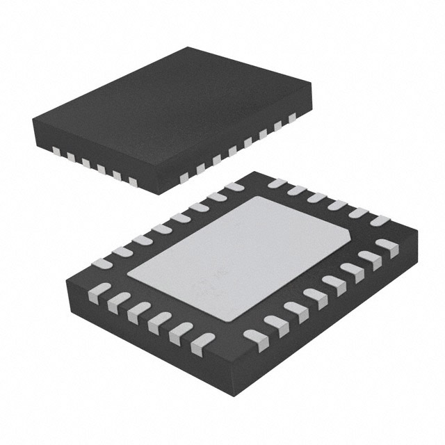
- Part No.:
- MPQ6532GVE-AEC1-P
- Manufacturer:
- Monolithic Power Systems Inc.
- Category:
- Motor Drivers, Controllers
- Package:
- 28-VFQFN Exposed Pad
- Datasheet:
-
 MPQ6532GVE-AEC1-P.pdf
- Description:
- 5V TO 60V, THREE-PHASE BRUSHLESS
- Quantity:
- Payment:

- Shipping:

Inventory:462
Please send an inquiry. Send us your inquiry, and we will respond immediately.
Product details
Overview
MPQ6532GVE-AEC1-P from Monolithic Power Systems is a three-phase BLDC motor pre-driver IC designed for automotive-grade motor control. It drives six N-channel MOSFETs across 5V–60V input, integrates 120° Hall-sensor commutation logic, supports 100% duty cycle via trickle-charged bootstrap, and delivers 0.8A HS source / 1A LS sink gate drive. Used in electric power steering pumps and HVAC blower actuators.
For engineers reviewing the MPQ6532GVE-AEC1-P datasheet, MPQ6532GVE-AEC1-P pinout, MPQ6532GVE-AEC1-P application, or MPQ6532GVE-AEC1-P equivalent, key selection criteria include AEC-Q100 Grade 1 qualification, configurable dead-time (700ns–5.7µs), VDS-based short-circuit protection with 3µs deglitch, LSS current-limit threshold (0.4–0.6V), and thermal shutdown at 190°C.
Technical Context
The MPQ6532GVE-AEC1-P implements integrated 120° commutation using three Hall sensor inputs (HA/HB/HC) with internal pull-down resistors, enabling direct interface to standard BLDC motor position sensors. Its gate drive architecture combines a regulated charge pump (VREG = 9.5–13V) for low-side drivers and bootstrap circuits (BSTA/BSTB/BSTC) with active trickle-charge to sustain high-side drive during 100% duty cycle operation.
Safety logic includes dual over-current detection: VDS sensing for short-circuit protection (SCP) triggered when drain-source voltage exceeds OC_REF (0.125–2.4V), and LSS shunt-based OCP with fixed 70µs off-time and 1µs HS minimum on-time. Fault reporting is handled via open-drain nFAULT with automatic latch-off until reset by nSLEEP or VIN UVLO recovery.
Key Specifications
| Parameter | Value and Actual Design Meaning |
|---|---|
| VIN Range | 5V to 60V - supports wide automotive battery range including cold-crank (5V) and load-dump transients (60V) |
| VREG Output | 9.5V to 13V - powers low-side gate drivers independently of VIN; enables reliable MOSFET turn-on down to 5V supply |
| Gate Drive Current | 0.8A source / 1A sink - sufficient to drive typical 10nC–50nC automotive MOSFETs at >20kHz PWM |
| Dead Time Control | 90ns to 5.7µs - adjustable via single RDT resistor; prevents shoot-through across all three phases simultaneously |
| OCP Threshold | 0.4V to 0.6V at LSS - sets motor stall current limit; scalable via external sense resistor value |
| Thermal Shutdown | 190°C with 30°C hysteresis - protects die during overload; resumes operation only after junction cools below 160°C |
| UVLO Threshold | 3.2V to 5V rising edge - disables all logic and gate outputs below valid supply; ensures clean startup above 3.9V nominal |
Pinout & Package
MPQ6532GVE-AEC1-P uses a thermally enhanced QFN-28 (4mm × 5mm) package with wettable flank and exposed thermal pad connected to GND. The 28-pin layout supports full three-phase gate drive, Hall sensor interface, fault signaling, and programmable protection functions.
| Pin/Terminal | Circuit Role | Design Meaning |
|---|---|---|
| VIN (Pin 1) | Main power input | Bypassed with 0.47µF + 10µF capacitors; must withstand 62V absolute max transient |
| BSTA/BSTB/BSTC (Pins 5,9,13) | Bootstrap supply nodes | Connect ceramic BST capacitors to SHA/SHB/SHC; enable high-side drive with trickle-charge support for 100% duty cycle |
| GHA/GHB/GHC (Pins 7,11,15) | High-side gate drivers | 0.8A source capability; drive external N-MOSFET gates with <1Ω pull-down resistance |
| GLA/GLB/GLC (Pins 8,12,16) | Low-side gate drivers | 1A sink capability; fast 2µs automatic LS turn-on at commutation edges |
| HA/HB/HC (Pins 20,19,18) | Hall sensor inputs | Internal 880kΩ pull-down; accept 3.3V/5V logic-level Hall signals spaced 120° mechanically |
| nFAULT (Pin 24) | Fault indicator | Open-drain output pulled low on SCP/OCP/thermal/UVLO fault; requires external pull-up |
| DT (Pin 27) | Dead time programming | Resistor-to-GND sets tDEAD from 90ns (RDT=0Ω) to 5.7µs (RDT=100kΩ); critical for shoot-through prevention |
Key Features
| Feature | Design Value |
|---|---|
| 120° Hall Commutation Logic | Eliminates need for external microcontroller-based commutation; reduces BOM count and firmware complexity in actuator designs |
| Trickle-Charged Bootstrap | Maintains HS-FET gate voltage during continuous conduction; enables true 100% duty cycle operation without external charge-pump IC |
| Configurable Short-Circuit Protection | VDS monitoring with 3µs deglitch window; prevents false triggering from switching transients while ensuring sub-10µs fault response |
| Adjustable Dead-Time Control | Single-resistor tuning across all three phases; simplifies layout and eliminates mismatch-induced shoot-through risk |
| AEC-Q100 Grade 1 Qualification | Validated for -40°C to +125°C ambient operation; meets automotive reliability, ESD (1.8kV HBM), and lifetime requirements |
Applications
| Electric Power Steering (EPS) Assist Pump | Automotive HVAC Blower Motor |
|---|---|
Use Scenario: Closed-loop torque assist in rack-and-pinion EPS systems requiring precise 3-phase motor control under varying load and temperature. IC Role / Device Role / Timing Role: Pre-driver executing Hall-based 120° commutation; interfaces directly to MCU PWM/DIR/nBRAKE commands while managing gate timing, dead time, and fault response. Use Value: Enables compact, high-efficiency pump design with integrated SCP and OCP-reducing external protection components and improving ASIL-B compliance readiness. | Use Scenario: Variable-speed cabin air circulation in passenger vehicles, operating continuously across -40°C to +85°C ambient with low acoustic noise requirements. IC Role / Device Role / Timing Role: Three-phase gate driver with sleep mode (2.5µA ISLEEP) and PWM speed control; manages thermal rise via 190°C shutdown and VREG regulation stability. Use Value: Delivers smooth low-RPM operation with 700ns–5.7µs dead-time tuning, minimizing torque ripple and audible switching noise in duct-mounted blowers. |
| Front Grille Shutter Actuator | Active Suspension Damping Valve |
Use Scenario: Position-controlled bi-directional actuation of aerodynamic grille shutters, requiring rapid start-stop cycles and stall current limiting. IC Role / Device Role / Timing Role: Motor controller with nBRAKE braking, DIR direction control, and LSS-based OCP; uses HA/HB/HC for position feedback and commutation sequencing. Use Value: Integrated motor start-up current limit and 70µs OCP off-time prevent inrush damage during frequent directional reversals at standstill. | Use Scenario: High-bandwidth, low-latency damping control in semi-active suspension systems where motor position must track real-time road inputs. IC Role / Device Role / Timing Role: Precision gate driver with <2µs LS turn-on latency and 1µs HS minimum on-time; synchronizes with vehicle CAN bus commanded PWM profiles. Use Value: Fast commutation response and stable VREG supply ensure consistent gate drive strength across 5V–60V battery fluctuations during aggressive cornering or braking events. |
Equivalent & Alternatives
The following parts are listed as comparable options for similar three-phase BLDC pre-driver applications.
| Alternative Part | Technical Difference | Application Difference | Selection Advice |
|---|---|---|---|
| DRV8305-Q1 | Integrated current-sense amplifiers; no external LSS shunt required; higher quiescent current (5mA vs. 4mA) | Preferred for designs needing inline phase current measurement without external op-amps | Select DRV8305-Q1 if closed-loop current control is mandatory; MPQ6532GVE-AEC1-P offers lower cost and simpler layout where shunt-based OCP suffices |
| MC33883 | Legacy 5V-only logic interface; no trickle-charge circuit; max VIN = 40V; lacks Hall-input integration | Requires external commutation logic and level-shifting for 12V+ systems | Choose MC33883 only for legacy 5V MCU platforms with existing design reuse; MPQ6532GVE-AEC1-P provides broader voltage range and integrated logic |
Compared with DRV8305-Q1 and MC33883, MPQ6532GVE-AEC1-P uniquely combines AEC-Q100 Grade 1 qualification, 5V–60V operation, Hall-integrated 120° commutation, and trickle-charged bootstrap in a single QFN-28 package-reducing system-level component count and PCB area while maintaining automotive thermal and fault robustness.
Availability
MPQ6532GVE-AEC1-P is available at Aetrix Electronics and suitable for automotive HVAC blowers, EPS assist pumps, front grille shutter actuators, and active suspension damping valves requiring stable component supply across extended temperature and lifecycle demands.
Supply support for MPQ6532GVE-AEC1-P includes scheduled delivery planning, volume procurement assistance, BOM continuity management, traceable sourcing, and lifecycle availability coordination for OEM customers, industrial embedded developers, connected-device designers, and electronics production programs.
Manufacturer
Monolithic Power Systems (MPS) is a fabless semiconductor company specializing in high-performance power management ICs, with design centers in the US, China, and Taiwan, and global manufacturing partnerships.
The MPQ6532 product line targets automotive-grade motor control applications, delivering integrated pre-driver functionality-including Hall commutation, gate drive, and fault protection-to simplify adoption in safety-critical electromechanical systems.
FAQ
What is the purpose of the trickle-charge circuit in MPQ6532GVE-AEC1-P?
The trickle-charge circuit maintains bootstrap capacitor (CBST) voltage during sustained high-side conduction, enabling true 100% duty cycle operation without external charge-pump ICs. It supplies ~5µA to counter leakage, ensuring reliable HS-FET gate drive even when LS-FETs remain off for extended periods-critical for holding torque in automotive actuators.
How does the MPQ6532GVE-AEC1-P implement short-circuit protection?
It uses VDS sensing on each MOSFET: when drain-to-source voltage exceeds the OC_REF reference (0.125–2.4V), a 3µs deglitched comparator triggers immediate gate drive disable and pulls nFAULT low. The device remains latched off until reset by nSLEEP deassertion or VIN UVLO recovery-preventing repeated fault cycling during persistent shorts.
Can MPQ6532GVE-AEC1-P operate without Hall sensors?
No-its commutation logic is hardwired for 120° Hall-input sequencing. Pins HA/HB/HC are mandatory inputs with internal pull-downs; floating them causes undefined behavior. For sensorless operation, an external MCU or dedicated sensorless driver IC is required upstream of the MPQ6532GVE-AEC1-P gate outputs.
What is the role of the LSS pin, and how is over-current protection set?
LSS is the low-side current-sense input. An external shunt resistor between LSS and the MOSFET source sets OCP threshold: VLSS-OCP = 0.4–0.6V defines the voltage trip point. When exceeded, the HS-FET turns off and LS-FET turns on for 70µs fixed off-time-limiting motor stall current without requiring external comparators or timers.
Is the DT pin compatible with standard resistor values for common dead-time requirements?
Yes-DT uses linear scaling: tDEAD (ns) ≈ 60 × RDT (kΩ). A 10kΩ resistor yields ~600ns (suitable for 100V-class MOSFETs), 20kΩ gives ~1.2µs (typical for 60V automotive systems), and 100kΩ achieves 5.7µs (for slower, high-RDS(ON) devices). Values are verified per datasheet Equation (1) and validated across temperature.
Does MPQ6532GVE-AEC1-P support both 3.3V and 5V logic interfaces?
Yes-input thresholds are VIL ≤ 0.8V and VIH ≥ 2.0V, accommodating both 3.3V and 5V CMOS logic families. All digital inputs (PWM, DIR, nBRAKE, nSLEEP, HA/HB/HC) have internal 880kΩ pull-downs, eliminating need for external biasing in most MCU interfacing scenarios.
What thermal derating applies to the QFN-28 package at elevated ambient temperatures?
With θJA = 40°C/W on a 4-layer PCB, maximum continuous power dissipation drops from 3.1W at 25°C to ~1.5W at 85°C ambient. Derating follows PD(MAX) = (150°C − TA)/40. Thermal pad soldering and copper pour area directly impact achievable power handling-designers must follow MPS layout guidelines for GND pad thermal vias and plane coverage.
MPQ6532GVE-AEC1-P Specifications
- Product attributes
- Attribute value
- Manufacturer:
- Monolithic Power Systems Inc.
- Series:
- -
- Package/Case:
- 28-VFQFN Exposed Pad
- Packaging:
- Tape & Reel (TR)
- Product Status:
- Active
- Motor Type - Stepper:
- Multiphase
- Motor Type - AC, DC:
- Brushless DC (BLDC)
- Function:
- Controller - Commutation, Direction Management
- Output Configuration:
- Pre-Driver - Half Bridge (3)
- Interface:
- PWM, Step/Direction
- Technology:
- Power MOSFET
- Step Resolution:
- -
- Applications:
- General Purpose
- Current - Output:
- 1A
- Voltage - Supply:
- 5V ~ 60V
- Voltage - Load:
- -
- Operating Temperature:
- -40°C ~ 150°C (TJ)
- Grade:
- Automotive
- Qualification:
- AEC-Q100
- Mounting Type:
- Surface Mount
- Supplier Device Package:
- 28-QFN (4x5)
MPQ6532GVE-AEC1-P FAQ
1.How can I place an order for MPQ6532GVE-AEC1-P through Aetrix?
Please submit a Request for Quotation (RFQ) for MPQ6532GVE-AEC1-P on Aetrix. Our sales agent will provide a competitive quotation and guide you through the order confirmation once you accept the terms.
2.Are the price and stock information for MPQ6532GVE-AEC1-P reliable?
The price and inventory of MPQ6532GVE-AEC1-P are updated periodically and may fluctuate due to market conditions. Stock and pricing data are typically refreshed every 24 hours. Quotation validity for MPQ6532GVE-AEC1-P is usually 5 days.
3.What payment methods are accepted for MPQ6532GVE-AEC1-P?
We accept Wire Transfer, PayPal, Credit Card, Western Union, MoneyGram, and Escrow for MPQ6532GVE-AEC1-P transactions.
Note: Certain payment methods may incur a processing fee.
4.How is shipping managed for MPQ6532GVE-AEC1-P?
MPQ6532GVE-AEC1-P orders can be shipped via leading logistics carriers, including DHL, UPS, FedEx, TNT, or Registered Mail.
Once your MPQ6532GVE-AEC1-P order is processed, you will receive an email with the shipment details and tracking number.
Note: Tracking information may take up to 24 hours to appear. Express delivery typically takes 3–5 business days.
5.How can I obtain technical support or documentation for MPQ6532GVE-AEC1-P?
For technical support, including MPQ6532GVE-AEC1-P datasheets, pinout diagrams, or application guidance, please contact our engineering support team. They can provide detailed documentation and assistance for your MPQ6532GVE-AEC1-P requirements.
6.How does Aetrix verify that MPQ6532GVE-AEC1-P is sourced from the original manufacturer or authorized distributors?
All MPQ6532GVE-AEC1-P products on Aetrix are procured from qualified distributors and authorized channels. Our dedicated quality assurance team conducts strict verification, including traceability checks and, if necessary, third-party testing. This ensures that MPQ6532GVE-AEC1-P meets industry standards.
7.What is the process for return or replacement of MPQ6532GVE-AEC1-P?
All MPQ6532GVE-AEC1-P units undergo pre-shipment inspection (PSI). If there is an issue with MPQ6532GVE-AEC1-P, returns or replacements are accepted under the following conditions:
1.Quantity discrepancies, incorrect items, or visible external defects (such as breakage or corrosion), acknowledged by Aetrix.
2.The issue is reported within 90 days of delivery.
3.The MPQ6532GVE-AEC1-P part is unused and in its original packaging.
Return procedure for MPQ6532GVE-AEC1-P:
1.Submit a request within 90 days.
2.Obtain a Return Material Authorization (RMA) from Aetrix.
MPQ6532GVE-AEC1-P Tags

-
DRV2603RUNR
Texas Instruments

-
DRV8837CDSGR
Texas Instruments

-
DRV8837DSGR
Texas Instruments
-
DRV8838DSGR
Texas Instruments

-
DRV8839DSSR
Texas Instruments

-
EMC2301-1-ACZL-TR
Microchip Technology
-
DRV8231ADSGR
Texas Instruments

-
EMC2302-2-AIZL-TR
Microchip Technology

-
DRV8800PWPR
Texas Instruments
-
DRV8835DSSR
Texas Instruments

-
EMC2303-1-KP-TR
Microchip Technology

-
DRV8876PWPR
Texas Instruments
Tech Hub

A practical engineering guide to 3.3V and 5V logic compatibility, input thresholds, resistor dividers, translator ICs, MOSFET level shifting, I2C pull-ups, timing limits and power-sequencing risks.

The 74HC595 uses push-pull logic outputs, while the TPIC6B595 uses 50 V open-drain DMOS sinks for higher-power loads. This guide compares timing, current limits, 3.3 V interfacing, load wiring, thermal…

The 74HC595 converts serial data into eight stable parallel outputs. This guide covers pin functions, shift and storage timing, OE and MR behavior, drive-current limits, cascading, voltage compatibilit…

A technical comparison of level-sensitive latches and edge-triggered flip-flops, covering timing windows, setup and hold limits, master–slave operation, time borrowing, race-through, HDL inference and…

A D latch stores one bit while Enable controls when data can pass. This reference covers gate-level operation, truth tables, transparency, setup and hold timing, LE versus OE, common ICs and practical …

An SR latch stores one bit through cross-coupled feedback. This engineering reference covers NOR and NAND implementations, truth tables, forbidden-state recovery, gated operation, switch debouncing, fa…

Latch circuits retain one bit through feedback. This technical reference covers SR and D latches, truth tables, transparency, timing limits, latch-versus-flip-flop behavior, applications and common log…

An engineering guide to LED driver operation, constant-current and constant-voltage outputs, linear and switching topologies, dimming, IC selection, calculations, replacement compatibility, and fault c…

Operational amplifier guide covering op amp basics, feedback, ideal vs real op amps, common configurations, buffer circuits, offset, bias current, gain-bandwidth, slew rate, rail-to-rail limits and sel…

Jumper cables guide covering safe connection order, red and black clamp placement, final ground connection, cable gauge, length, clamp quality, copper vs CCA cables, jump starter comparison and battery…


