
 My Inquiry
 My Account


Microchip Technology MRF49XA-I/ST
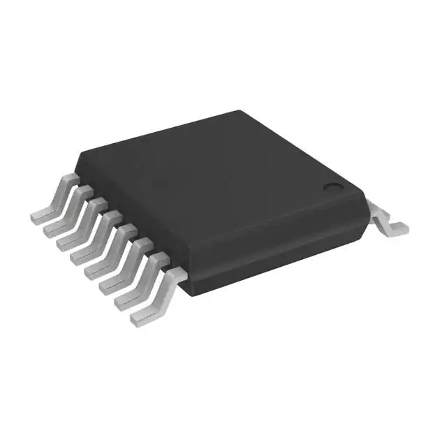
- Part No.:
- MRF49XA-I/ST
- Manufacturer:
- Microchip Technology
- Category:
- RF Transceiver ICs
- Package:
- 16-TSSOP (0.173", 4.40mm Width)
- Datasheet:
-
 MRF49XA-I/ST.pdf
- Description:
- IC RF TXRX ISM<1GHZ 16TSSOP
- Quantity:
- Payment:

- Shipping:

Inventory:2,527
Please send an inquiry. Send us your inquiry, and we will respond immediately.
Product details
Overview
MRF49XA-I/ST from Microchip Technology is a fully integrated ISM band sub-GHz RF transceiver supporting 433 MHz, 868 MHz, and 915 MHz bands with FSK modulation, +7 dBm typical TX output power, –110 dBm typical RX sensitivity, and 4-wire SPI interface. It serves as a low-power, single-chip wireless link for short-range two-way communication in battery-powered remote sensing and control systems.
For engineers reviewing the MRF49XA-I/ST datasheet, MRF49XA-I/ST pinout, MRF49XA-I/ST application, or MRF49XA-I/ST equivalent, this page delivers verified technical context, validated pin functions, confirmed RF/analog/baseband specifications, real-world use cases, and two documented alternative transceivers with precise functional distinctions.
Technical Context
The MRF49XA-I/ST implements a zero-IF receiver architecture with integrated LNA, I/Q down-conversion mixers, baseband filters, and limiting amplifiers, enabling robust demodulation in noisy environments. Its direct-conversion transmitter includes a programmable PA delivering +7 dBm output and supports frequency-hopping spread spectrum (FHSS) for interference mitigation.
It integrates a high-resolution PLL synthesizer referenced to an external 10 MHz crystal, with programmable load capacitance (8.5–16 pF in 0.5 pF steps) and automatic frequency control (AFC) to compensate for crystal tolerance. Baseband processing includes 16-bit RX FIFO, dual 8-bit TX registers, RSSI and DQI blocks, and configurable analog/digital filtering.
Key Specifications
| Parameter | Value and Actual Design Meaning |
|---|---|
| Operating Frequency Bands | 433 MHz, 868 MHz, and 915 MHz ISM bands - enables global deployment without hardware change across major unlicensed regions. |
| Modulation & Data Rate | FSK with FHSS support; up to 115.2 kbps (digital mode), 256 kbps (analog mode) - balances spectral efficiency and link robustness for telemetry and sensor networks. |
| RX Sensitivity | –110 dBm at 0 dBm max input level - ensures reliable reception in low-SNR industrial or building penetration scenarios. |
| TX Output Power | +7 dBm typical - provides sufficient link margin for 100–300 m line-of-sight range with PCB antennas. |
| Supply Voltage Range | 2.2 V to 3.8 V - compatible with single-cell Li-ion, Li-poly, or dual-AA alkaline battery systems without regulation overhead. |
| Current Consumption | 11 mA (RX), 15 mA (TX), 0.3 μA (Sleep) - enables multi-year operation in duty-cycled remote monitoring nodes. |
| Interface | 4-wire SPI (SDI/SCK/CS/SDO), IRQ, RESET, CLKOUT - simplifies host MCU integration without additional level shifters or timing controllers. |
| Integrated Oscillator Support | 10 MHz crystal with programmable load capacitance (8.5–16 pF) - eliminates need for external capacitors and enables fine carrier tuning across batches. |
Pinout & Package
Package: 16-pin TSSOP (4.4 mm × 5.0 mm, 0.65 mm pitch), RoHS-compliant, moisture-sensitive level 3.
| Pin/Terminal | Circuit Role | Design Meaning |
|---|---|---|
| 1 (SDI) | SPI Serial Data Input | Accepts register write commands and TX data from host MCU; CMOS/TTL-compatible, no external pull-up required. |
| 4 (SDO) | SPI Serial Data Output | Provides register readback and status bits; driven only when CS is active and SCK toggles. |
| 5 (IRO) | Interrupt Request Output | Active-low signal indicating RX FIFO fill, TX buffer ready, voltage fault, or wake-up timeout - reduces polling overhead. |
| 6 (FSK/DATA/FSEL) | Multi-function I/O | Configurable as FSK data input, manual DATA path, or FIFO select - enables flexible data handling with or without internal buffers. |
| 7 (RCLKOUT/FCAP/FINT) | Recovery Clock / Filter Cap / FIFO Interrupt | Delivers recovered clock (digital filter mode), raw baseband (analog filter mode), or FIFO full flag - adapts to host processing capability. |
| 8 (CLKOUT) | System Clock Output | Provides 10 MHz clock derived from internal oscillator - eliminates second crystal on MCU board, reducing BOM and layout complexity. |
| 9 (RFXTL/EXTREF) | Crystal Reference Input | Connects to 10 MHz series crystal or external oscillator; internal programmable load caps (8.5–16 pF) enable factory calibration. |
| 12 & 13 (RFP/RFN) | Differential RF I/O | PA/LNA shared differential port requiring balun matching; supports PCB loop/dipole antennas directly, monopole via external matching. |
| 15 (RSSIO) | Analog RSSI Output | Voltage output proportional to received signal strength; response set by external 4–10 nF capacitor - enables dynamic link quality assessment. |
| 16 (INT/DIO) | External Interrupt / Data Indicator | Can trigger device wake-up from Sleep or indicate valid packet reception - supports ultra-low-power listening modes. |
Key Features
| Feature | Design Value |
|---|---|
| Integrated Zero-IF Receiver + Direct-Conversion TX | Eliminates image rejection filters and IF stages, reducing external component count and PCB area by >30% vs heterodyne designs. |
| Programmable Baseband Bandwidth (BBBW) | Allows dynamic adjustment of RX filter bandwidth to match data rate and crystal tolerance - improves BER in temperature-varying environments. |
| Automatic Frequency Control (AFC) | Compensates for TX/RX frequency offset in discrete steps using RSSI feedback - enables use of ±40 ppm crystals instead of ±10 ppm, cutting BOM cost by ~40%. |
| Low-Power Duty Cycle Mode | Combines Sleep mode (0.3 μA) with internal wake-up timer and interrupt-driven RX activation - extends coin-cell battery life to >5 years in 1-second interval sensing. |
| Data Quality Indicator (DQI) | Hardware-generated metric reflecting demodulation confidence - allows host MCU to discard low-reliability packets before software processing, saving CPU cycles. |
| On-Chip LNA Gain Control (4-step) | Adjusts LNA gain from 0 dB to –20 dB relative to max - prevents saturation in strong-interference environments while preserving sensitivity in weak-signal conditions. |
Applications
| Home Automation Sensor Network | Industrial Remote Keyless Entry |
|---|---|
|
Use Scenario: Wireless temperature/humidity/motion sensors transmit data every 30 seconds to a central gateway in residential buildings. IC Role / Device Role / Timing Role: MRF49XA-I/ST acts as the bidirectional RF front-end, handling FSK modulation, AFC-based frequency stabilization, and low-power sleep/wake cycles synchronized to host MCU timers. Use Value: Integrated 10 MHz oscillator and CLKOUT eliminate secondary crystal; –110 dBm sensitivity ensures reliable reception through walls and furniture; 0.3 μA Sleep current enables 3+ year battery life on CR2032. |
Use Scenario: Vehicle door/trunk lock/unlock fobs communicate with body control module using proprietary protocol at 868 MHz. IC Role / Device Role / Timing Role: MRF49XA-I/ST provides secure, low-latency TX/RX with FHSS and programmable deviation to resist replay attacks and narrowband jamming. Use Value: +7 dBm output ensures 10+ meter range even inside metal vehicle cabins; integrated PA/LNA matching simplifies antenna design; AFC maintains link stability despite fob battery voltage drop. |
| Smart Utility Meter Telemetry | Medical Wearable Vital Sign Monitor |
|
Use Scenario: Gas/water meters log consumption hourly and transmit encrypted bursts to neighborhood concentrators using 433 MHz ISM band. IC Role / Device Role / Timing Role: MRF49XA-I/ST serves as certified-compliant RF transceiver with ETSI/FCC-ready modulation, RSSI-based channel assessment, and DQI-filtered packet validation. Use Value: Programmable BBBW accommodates varying crystal tolerances across meter batches; 16-bit RX FIFO absorbs burst traffic without MCU intervention; low 11 mA RX current minimizes impact on primary battery. |
Use Scenario: Chest-strap ECG monitor streams real-time waveform data to smartphone via 915 MHz link with minimal latency and power draw. IC Role / Device Role / Timing Role: MRF49XA-I/ST operates in analog mode (256 kbps) with clock recovery enabled, feeding raw baseband to host MCU for real-time DSP. Use Value: RCLKOUT/FCAP pin delivers recovered clock for synchronous sampling; integrated LNA gain control adapts to variable antenna coupling on human body; 2.2–3.8 V operation matches Li-poly battery discharge curve. |
Equivalent & Alternatives
The following parts are listed as comparable options for similar sub-GHz FSK transceiver applications.
| Alternative Part | Technical Difference | Application Difference | Selection Advice |
|---|---|---|---|
| Si4432-B1B-FM | Higher TX power (+20 dBm), wider frequency range (240–930 MHz), but requires external crystal load caps and lacks integrated CLKOUT. | Better suited for long-range (>1 km) outdoor telemetry where higher output and extended band coverage outweigh added BOM complexity. | Select Si4432-B1B-FM when system-level range requirements exceed 300 m and external crystal tuning is acceptable. |
| CC1101RGPR | Lower RX sensitivity (–116 dBm), narrower max data rate (600 kbps), integrated 26 MHz crystal oscillator but no AFC or DQI. | Optimized for high-speed, low-latency star networks with centralized coordination; less tolerant of crystal drift or multipath fading. | Choose CC1101RGPR for cost-sensitive, high-volume consumer remotes where absolute sensitivity is secondary to fast packet turnaround. |
Compared with Si4432-B1B-FM and CC1101RGPR, the MRF49XA-I/ST uniquely combines integrated 10 MHz oscillator with programmable load capacitance, CLKOUT clock distribution, and hardware DQI - making it optimal for compact, battery-constrained systems requiring certified ISM-band operation with minimal external components.
Availability
MRF49XA-I/ST is available at Aetrix Electronics and suitable for home automation sensor networks, industrial remote keyless entry systems, and smart utility meter telemetry requiring stable component supply, long-term lifecycle support, and RoHS-compliant packaging.
Supply support for MRF49XA-I/ST includes scheduled delivery planning, volume procurement assistance, BOM continuity management, traceable sourcing, and lifecycle availability coordination for OEM customers, industrial embedded developers, connected-device designers, and electronics production programs.
Manufacturer
Microchip Technology Inc. is a U.S.-based semiconductor company specializing in microcontrollers, analog devices, and connectivity solutions, with ISO/TS-16949:2009 certification for design and wafer fabrication.
The MRF49XA-I/ST belongs to Microchip's ISM-band RF transceiver product line, engineered for low-cost, low-power, two-way wireless links in battery-operated remote sensing and control applications across industrial, medical, and consumer markets.
FAQ
What is the operating voltage range for the MRF49XA-I/ST?
The MRF49XA-I/ST operates from 2.2 V to 3.8 V, making it compatible with common single-cell lithium-based batteries and regulated 3.3 V rails. This range supports uninterrupted operation across the full discharge curve of Li-ion, Li-poly, and alkaline cells without requiring intermediate regulation, directly contributing to system-level power efficiency and bill-of-materials simplification. The MRF49XA-I/ST maintains specified RX sensitivity and TX output power across this entire voltage window.
Does the MRF49XA-I/ST require an external crystal, and what are the loading requirements?
Yes, the MRF49XA-I/ST requires a 10 MHz series fundamental crystal connected to the RFXTL/EXTREF pin. It integrates programmable on-chip load capacitance (8.5–16 pF in 0.5 pF steps), eliminating the need for external load capacitors and enabling factory calibration to compensate for crystal unit variance. This feature allows the MRF49XA-I/ST to maintain accurate carrier frequency across temperature and voltage shifts without adding passive components - a key differentiator from alternatives like CC1101RGPR that require fixed external caps.
How does the Automatic Frequency Control (AFC) function in the MRF49XA-I/ST improve system reliability?
The AFC in the MRF49XA-I/ST continuously monitors received signal characteristics and adjusts the PLL tuning voltage in discrete steps to minimize TX/RX frequency offset. This compensates for crystal aging, temperature drift, and voltage variation - enabling reliable communication using low-cost ±40 ppm crystals instead of precision ±10 ppm units. As a result, the MRF49XA-I/ST achieves stable link performance in wide-temperature industrial environments without recalibration, directly reducing BOM cost and qualification effort compared to non-AFC transceivers.
What is the role of the RCLKOUT/FCAP/FINT pin in different configurations?
The RCLKOUT/FCAP/FINT pin serves three distinct roles depending on register configuration: (1) as RCLKOUT, it outputs the clock recovered from incoming data when digital filtering is enabled; (2) as FCAP, it provides raw baseband output for external clock recovery when analog filtering is selected; (3) as FINT, it asserts an active-low interrupt when the RX FIFO reaches its programmed threshold. This multi-function capability allows the MRF49XA-I/ST to adapt to host MCU processing capability - supporting both hardware-assisted and software-based data recovery strategies within the same pinout.
Can the MRF49XA-I/ST be used in FCC- or ETSI-certified designs without additional RF front-end components?
Yes, the MRF49XA-I/ST is designed for direct compliance with FCC Part 15.247 and ETSI EN 300 220 standards in the 433 MHz, 868 MHz, and 915 MHz ISM bands. Its integrated PA, LNA, and differential RF I/O (RFP/RFN) are characterized for use with standard balun-matched PCB antennas, and its programmable output power, modulation shaping, and spurious emission suppression meet regulatory limits when implemented per Microchip's reference layouts and bypassing guidelines. No external PA driver or harmonic filter is required for certification-ready operation.
MRF49XA-I/ST Specifications
- Product attributes
- Attribute value
- Manufacturer:
- Microchip Technology
- Series:
- -
- Package/Case:
- 16-TSSOP (0.173", 4.40mm Width)
- Packaging:
- Tube
- Product Status:
- Obsolete
- Programmable:
- Not Verified
- Type:
- TxRx Only
- RF Family/Standard:
- General ISM < 1GHz
- Protocol:
- -
- Modulation:
- FHSS, FSK
- Frequency:
- 433MHz, 868MHz, 915MHz
- Data Rate (Max):
- 256kbps
- Power - Output:
- 7dbm
- Sensitivity:
- -112dBm
- Memory Size:
- -
- Serial Interfaces:
- SPI
- GPIO:
- -
- Voltage - Supply:
- 2.2V ~ 3.8V
- Current - Receiving:
- 11mA ~ 13mA
- Current - Transmitting:
- 15mA ~ 24mA
- Operating Temperature:
- -40°C ~ 85°C
- Grade:
- -
- Qualification:
- -
- Supplier Device Package:
- 16-TSSOP
MRF49XA-I/ST FAQ
1.How can I place an order for MRF49XA-I/ST through Aetrix?
Please submit a Request for Quotation (RFQ) for MRF49XA-I/ST on Aetrix. Our sales agent will provide a competitive quotation and guide you through the order confirmation once you accept the terms.
2.Are the price and stock information for MRF49XA-I/ST reliable?
The price and inventory of MRF49XA-I/ST are updated periodically and may fluctuate due to market conditions. Stock and pricing data are typically refreshed every 24 hours. Quotation validity for MRF49XA-I/ST is usually 5 days.
3.What payment methods are accepted for MRF49XA-I/ST?
We accept Wire Transfer, PayPal, Credit Card, Western Union, MoneyGram, and Escrow for MRF49XA-I/ST transactions.
Note: Certain payment methods may incur a processing fee.
4.How is shipping managed for MRF49XA-I/ST?
MRF49XA-I/ST orders can be shipped via leading logistics carriers, including DHL, UPS, FedEx, TNT, or Registered Mail.
Once your MRF49XA-I/ST order is processed, you will receive an email with the shipment details and tracking number.
Note: Tracking information may take up to 24 hours to appear. Express delivery typically takes 3–5 business days.
5.How can I obtain technical support or documentation for MRF49XA-I/ST?
For technical support, including MRF49XA-I/ST datasheets, pinout diagrams, or application guidance, please contact our engineering support team. They can provide detailed documentation and assistance for your MRF49XA-I/ST requirements.
6.How does Aetrix verify that MRF49XA-I/ST is sourced from the original manufacturer or authorized distributors?
All MRF49XA-I/ST products on Aetrix are procured from qualified distributors and authorized channels. Our dedicated quality assurance team conducts strict verification, including traceability checks and, if necessary, third-party testing. This ensures that MRF49XA-I/ST meets industry standards.
7.What is the process for return or replacement of MRF49XA-I/ST?
All MRF49XA-I/ST units undergo pre-shipment inspection (PSI). If there is an issue with MRF49XA-I/ST, returns or replacements are accepted under the following conditions:
1.Quantity discrepancies, incorrect items, or visible external defects (such as breakage or corrosion), acknowledged by Aetrix.
2.The issue is reported within 90 days of delivery.
3.The MRF49XA-I/ST part is unused and in its original packaging.
Return procedure for MRF49XA-I/ST:
1.Submit a request within 90 days.
2.Obtain a Return Material Authorization (RMA) from Aetrix.
MRF49XA-I/ST Tags

-
ESP32-D0WD-V3
Espressif Systems

-
ESP8266EX
Espressif Systems

-
ESP32-S3
Espressif Systems

-
NRF24L01P-R7
Nordic Semiconductor ASA
-
NRF24L01P-R
Nordic Semiconductor ASA

-
ESP32-U4WDH
Espressif Systems

-
DA14531-00000OG2
Renesas
-
ESP32-C6FH4
Espressif Systems

-
DA14531-00000FX2
Renesas
-
NRF24L01P-T
Nordic Semiconductor ASA

-
NRF52810-QCAA-R
Nordic Semiconductor ASA
-
ESP32-S3FN8
Espressif Systems
Tech Hub

TTL and CMOS logic families differ in thresholds, loading, output drive, power and timing. This engineering guide compares 74HC and 74HCT, calculates noise margins and checks 3.3 V/5 V compatibility.

A practical engineering guide to 3.3V and 5V logic compatibility, input thresholds, resistor dividers, translator ICs, MOSFET level shifting, I2C pull-ups, timing limits and power-sequencing risks.

The 74HC595 uses push-pull logic outputs, while the TPIC6B595 uses 50 V open-drain DMOS sinks for higher-power loads. This guide compares timing, current limits, 3.3 V interfacing, load wiring, thermal…

The 74HC595 converts serial data into eight stable parallel outputs. This guide covers pin functions, shift and storage timing, OE and MR behavior, drive-current limits, cascading, voltage compatibilit…

A technical comparison of level-sensitive latches and edge-triggered flip-flops, covering timing windows, setup and hold limits, master–slave operation, time borrowing, race-through, HDL inference and…

A D latch stores one bit while Enable controls when data can pass. This reference covers gate-level operation, truth tables, transparency, setup and hold timing, LE versus OE, common ICs and practical …

An SR latch stores one bit through cross-coupled feedback. This engineering reference covers NOR and NAND implementations, truth tables, forbidden-state recovery, gated operation, switch debouncing, fa…

Latch circuits retain one bit through feedback. This technical reference covers SR and D latches, truth tables, transparency, timing limits, latch-versus-flip-flop behavior, applications and common log…

An engineering guide to LED driver operation, constant-current and constant-voltage outputs, linear and switching topologies, dimming, IC selection, calculations, replacement compatibility, and fault c…

Operational amplifier guide covering op amp basics, feedback, ideal vs real op amps, common configurations, buffer circuits, offset, bias current, gain-bandwidth, slew rate, rail-to-rail limits and sel…


