
 My Inquiry
 My Account


Texas Instruments MSP430F122IDWR
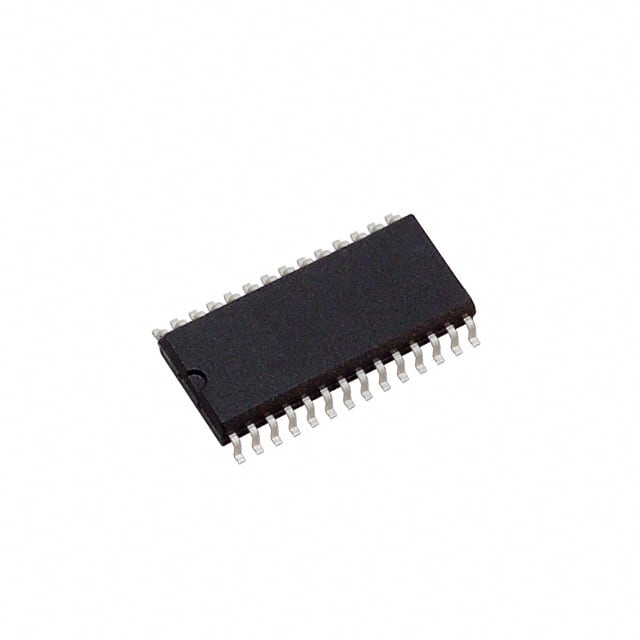
- Part No.:
- MSP430F122IDWR
- Manufacturer:
- Texas Instruments
- Category:
- Microcontrollers
- Package:
- 28-SOIC (0.295", 7.50mm Width)
- Datasheet:
-
 MSP430F122IDWR.pdf
- Description:
- IC MCU 16BIT 4KB FLASH 28SOIC
- Quantity:
- Payment:

- Shipping:

Inventory:4,692
Please send an inquiry. Send us your inquiry, and we will respond immediately.
Product details
Overview
MSP430F122IDWR from Texas Instruments is an ultralow-power 16-bit RISC mixed-signal microcontroller featuring 4KB Flash + 256B RAM, 22 I/O pins, a 16-bit Timer_A with three capture/compare registers, on-chip analog comparator, and USART0 supporting UART/SPI protocols. It operates from 1.8 V to 3.6 V and targets battery-powered sensor systems requiring sub-μA standby current and fast wake-up.
For engineers reviewing the MSP430F122IDWR datasheet, MSP430F122IDWR pinout, MSP430F122IDWR application, or MSP430F122IDWR equivalent, key selection criteria include its 0.7 μA standby current, <6 μs wake-up from LPM3, integrated slope A/D capability via comparator, and 28-pin TSSOP (PW) package compatibility confirmed for this variant.
Technical Context
The MSP430F122IDWR implements a 16-bit RISC CPU with constant generators and seven addressing modes, enabling single-cycle register operations. Its basic clock module supports multiple sources: internal DCO (stabilizes in <6 μs), 32 kHz crystal, external resistor, or high-frequency crystal - all selectable via BCSCTL registers.
Peripherals are memory-mapped and accessible via full instruction set. The device integrates Timer_A3 with three independent capture/compare registers (TACCR0–2), a comparator_A module usable for analog signal comparison or single-slope A/D conversion, and USART0 with dual-buffered TX/RX supporting software-selectable UART or SPI mode.
Key Specifications
| Parameter | Value and Actual Design Meaning |
|---|---|
| Core Architecture | 16-bit RISC CPU with 16 general-purpose registers and constant generators; enables efficient code execution and low cycle-per-instruction overhead. |
| Memory | 4KB Flash program memory + 256B RAM; supports in-system programming and BSL-based UART flash loading without external voltage. |
| Supply Voltage | 1.8 V to 3.6 V operating range; allows direct integration with single-cell Li-ion or two-cell alkaline batteries. |
| Active Current | 200 μA at 1 MHz, 2.2 V; defines baseline power budget for continuous sensor sampling and processing. |
| Standby Current | 0.7 μA in LPM3 mode; enables multi-year operation in intermittently active sensor nodes. |
| Wake-up Time | <6 μs from LPM3 to active mode; ensures timely response to external interrupts (e.g., motion or threshold events). |
| I/O Count | 22 programmable digital I/O pins across Ports P1–P3; includes interrupt-capable edges on P1 and P2 for event-driven wake-up. |
Pinout & Package
Package: 28-pin Plastic Thin Shrink Small-Outline Package (TSSOP), suffix PW - confirmed for MSP430F122IDWR per device marking and availability table.
| Pin/Terminal | Circuit Role | Design Meaning |
|---|---|---|
| P1.0/TACLK | Timer_A clock input / GPIO | Accepts external timing source for Timer_A; configurable as general-purpose I/O with interrupt capability. |
| P1.1/TA0 | Timer_A CCI0A input / GPIO / BSL TX | Primary capture/compare channel 0; also serves as bootstrap loader transmit pin during serial programming. |
| P1.2/TA1 | Timer_A CCI1A input / GPIO | Second capture/compare channel; supports PWM generation or input capture with independent control. |
| P1.3/TA2 | Timer_A CCI2A input / GPIO | Third capture/compare channel; enables simultaneous timing of three independent events or waveforms. |
| P2.2/CAOUT/TA0 | Comparator_A output / Timer_A CCI0B input | Provides comparator result as logic-level output; also feeds into Timer_A channel 0 for slope A/D conversion triggering. |
| P2.3/CA0/TA1 | Comparator_A input A / Timer_A CCI1B input | Analog input for comparator reference or signal; dual-use enables hardware-assisted analog measurement without CPU intervention. |
| P3.4/UTXD0 | USART0 UART transmit / GPIO | Drives serial data to host MCU or radio module; supports asynchronous communication at configurable baud rates. |
| RST/NMI | Reset or non-maskable interrupt input | Hardware reset initiation or critical fault handling; level-sensitive with internal pullup; triggers power-on reset sequence. |
Key Features
| Feature | Design Value |
|---|---|
| Five Low-Power Modes (LPM0–LPM4) | Enables precise trade-off between peripheral activity and current draw - e.g., LPM3 retains ACLK and RAM while disabling CPU and SMCLK for ultra-low sleep current. |
| Digital Controlled Oscillator (DCO) | Provides factory-trimmed internal clock source that stabilizes in <6 μs, eliminating need for external crystal in cost-sensitive designs. |
| Integrated Analog Comparator | Supports battery voltage monitoring, resistive sensor interface, and single-slope A/D conversion - no external ADC required for basic analog thresholding. |
| Serial Onboard Programming (BSL) | Allows field firmware updates via UART using only P1.1 (TX) and P2.2 (RX); eliminates need for JTAG debugger in production deployment. |
| Programmable Code Protection | Security fuse prevents unauthorized read-out of Flash contents, protecting proprietary algorithms and calibration data in deployed devices. |
Applications
| Wireless Sensor Node | Portable Medical Monitor |
|---|---|
Use Scenario: Battery-powered temperature/humidity node transmitting data via sub-GHz RF transceiver every 5 minutes. IC Role / Device Role / Timing Role: Main system controller managing sensor reads, data formatting, low-power scheduling, and UART-to-RF handoff. Use Value: 0.7 μA LPM3 current extends 2xAA battery life beyond 5 years; <6 μs wake-up ensures accurate timing of RF transmission windows. | Use Scenario: Wearable pulse oximeter acquiring analog photodiode signals and calculating SpO₂ in real time. IC Role / Device Role / Timing Role: Mixed-signal processor performing analog comparator-based slope A/D on photodiode outputs and driving OLED display via SPI. Use Value: On-chip comparator eliminates external ADC; 22 GPIOs support LED drivers, button inputs, and display interface with minimal BOM count. |
| Industrial Data Logger | Smart Meter Interface Module |
Use Scenario: DIN-rail mounted logger capturing voltage/current samples from CTs and PTs at 1 kHz, storing to EEPROM. IC Role / Device Role / Timing Role: Precision timing controller synchronizing ADC sampling to line cycle using Timer_A and ACLK from 32.768 kHz crystal. Use Value: 16-bit Timer_A with three capture/compare registers enables simultaneous timestamping, PWM generation for isolation drivers, and interval timing for EEPROM writes. | Use Scenario: Communication bridge between utility meter ASIC and PLC/HPLC modem, translating proprietary protocol to DLMS over UART. IC Role / Device Role / Timing Role: Protocol translation engine handling UART framing, checksum calculation, and SPI-controlled modem register access. Use Value: Dual-mode USART0 supports both UART (to meter) and SPI (to modem) simultaneously; 4KB Flash accommodates dual-stack firmware and encryption routines. |
Equivalent & Alternatives
The following parts are listed as comparable options for similar mixed-signal microcontroller applications.
| Alternative Part | Technical Difference | Application Difference | Selection Advice |
|---|---|---|---|
| MSP430F123IDWR | 8KB Flash + 256B RAM; identical peripherals, package, and pinout. | Supports larger firmware images and more complex protocol stacks without external memory. | Select when firmware size exceeds 4KB or future scalability is required; same PCB layout and power design. |
| MSP430F2274IRHBT | 16KB Flash + 1KB RAM; enhanced USCI module (replaces USART0); 40-pin QFN package. | Higher memory capacity and improved serial peripheral flexibility, but requires PCB redesign due to different pin count and layout. | Choose for new designs needing >4KB code space or USCI's IrDA/ LIN support; not drop-in compatible with MSP430F122IDWR. |
Compared with MSP430F122IDWR, MSP430F123IDWR offers double Flash capacity with zero hardware changes, while MSP430F2274IRHBT provides expanded memory and serial capabilities at the cost of board redesign - making the F122 optimal for cost-constrained, volume-sensitive sensor endpoints where 4KB suffices.
Availability
MSP430F122IDWR is available at Aetrix Electronics and suitable for wireless sensor nodes, portable medical monitors, and industrial data loggers requiring stable component supply and long-term lifecycle support.
Supply support for MSP430F122IDWR includes scheduled delivery planning, volume procurement assistance, BOM continuity management, traceable sourcing, and lifecycle availability coordination for OEM customers, industrial embedded developers, connected-device designers, and electronics production programs.
Manufacturer
Texas Instruments is a global semiconductor leader specializing in analog, embedded processing, and connectivity technologies with decades of microcontroller innovation.
The MSP430x12x product line was designed specifically for ultralow-power, battery-operated measurement applications - emphasizing rapid wake-up, integrated analog peripherals, and minimal active/sleep current across five power modes.
FAQ
What is the maximum operating frequency of the MSP430F122IDWR at 3.6 V?
The MSP430F122IDWR supports a maximum system clock (MCLK) frequency of 8 MHz when VCC = 3.6 V, as specified in the recommended operating conditions table. This limit applies to CPU and peripheral timing; higher frequencies are not guaranteed and may cause instability or increased current consumption beyond datasheet specifications. The MSP430F122IDWR achieves this using its internal DCO or external crystal sources, with appropriate BCSCTL register configuration.
Does the MSP430F122IDWR support in-system programming without a JTAG interface?
Yes, the MSP430F122IDWR supports in-system programming via its built-in Bootstrap Loader (BSL), which uses UART communication on P1.1 (TX) and P2.2 (RX). No external programming voltage is required, and the BSL is activated by specific entry sequences on reset. This enables field firmware updates without JTAG hardware, though JTAG remains available for full debug and flash programming via TEST, TCK, TMS, and TDI pins.
How many capture/compare channels does Timer_A provide on the MSP430F122IDWR?
The MSP430F122IDWR includes Timer_A3 - a 16-bit timer with three independent capture/compare registers (TACCR0, TACCR1, TACCR2), each supporting both input capture and output compare functions. These registers map to dedicated pins including P1.1/TA0, P1.2/TA1, and P1.3/TA2, enabling simultaneous PWM generation, input edge timing, and interval measurement without CPU overhead.
What is the function of the P2.5/ROSC pin on the MSP430F122IDWR?
The P2.5/ROSC pin on the MSP430F122IDWR serves as the input for an external resistor that sets the nominal frequency of the internal digitally controlled oscillator (DCO). Connecting a resistor between P2.5/ROSC and VSS configures the DCO's base frequency, allowing clock tuning without crystals. This pin is bidirectional and can also operate as a general-purpose I/O when the DCO resistor configuration is not used.
Is the MSP430F122IDWR pin-compatible with other packages in the MSP430F12x family?
The MSP430F122IDWR is supplied in the 28-pin TSSOP (PW) package and shares identical pin functions and numbering with the 28-pin SOWB (DW) variant (e.g., MSP430F122IDW), as confirmed by the shared pin designation table. However, it is not pin-compatible with the 32-pin QFN (RHB) variant due to differing pin count, layout, and NC pin assignments - requiring separate PCB designs for each package type.
MSP430F122IDWR Specifications
- Product attributes
- Attribute value
- Manufacturer:
- Texas Instruments
- Package/Case:
- 28-SOIC (0.295", 7.50mm Width)
- Series:
- MSP430x1xx
- Packaging:
- Tape & Reel (TR)
- Product Status:
- Obsolete
- Programmable:
- Not Verified
- Core Processor:
- MSP430 CPU16
- Core Size:
- 16-Bit
- Speed:
- 8MHz
- Connectivity:
- SPI, UART/USART
- Peripherals:
- POR, PWM, WDT
- Number of I/O:
- 22
- Program Memory Size:
- 4KB (4K x 8 + 256B)
- Program Memory Type:
- FLASH
- EEPROM Size:
- -
- RAM Size:
- 256 x 8
- Voltage - Supply (Vcc/Vdd):
- 1.8V ~ 3.6V
- Data Converters:
- Slope A/D
- Oscillator Type:
- Internal
- Operating Temperature:
- -40°C ~ 85°C (TA)
- Grade:
- -
- Qualification:
- -
- Mounting Type:
- Surface Mount
- Supplier Device Package:
MSP430F122IDWR FAQ
1.How can I place an order for MSP430F122IDWR through Aetrix?
Please submit a Request for Quotation (RFQ) for MSP430F122IDWR on Aetrix. Our sales agent will provide a competitive quotation and guide you through the order confirmation once you accept the terms.
2.Are the price and stock information for MSP430F122IDWR reliable?
The price and inventory of MSP430F122IDWR are updated periodically and may fluctuate due to market conditions. Stock and pricing data are typically refreshed every 24 hours. Quotation validity for MSP430F122IDWR is usually 5 days.
3.What payment methods are accepted for MSP430F122IDWR?
We accept Wire Transfer, PayPal, Credit Card, Western Union, MoneyGram, and Escrow for MSP430F122IDWR transactions.
Note: Certain payment methods may incur a processing fee.
4.How is shipping managed for MSP430F122IDWR?
MSP430F122IDWR orders can be shipped via leading logistics carriers, including DHL, UPS, FedEx, TNT, or Registered Mail.
Once your MSP430F122IDWR order is processed, you will receive an email with the shipment details and tracking number.
Note: Tracking information may take up to 24 hours to appear. Express delivery typically takes 3–5 business days.
5.How can I obtain technical support or documentation for MSP430F122IDWR?
For technical support, including MSP430F122IDWR datasheets, pinout diagrams, or application guidance, please contact our engineering support team. They can provide detailed documentation and assistance for your MSP430F122IDWR requirements.
6.How does Aetrix verify that MSP430F122IDWR is sourced from the original manufacturer or authorized distributors?
All MSP430F122IDWR products on Aetrix are procured from qualified distributors and authorized channels. Our dedicated quality assurance team conducts strict verification, including traceability checks and, if necessary, third-party testing. This ensures that MSP430F122IDWR meets industry standards.
7.What is the process for return or replacement of MSP430F122IDWR?
All MSP430F122IDWR units undergo pre-shipment inspection (PSI). If there is an issue with MSP430F122IDWR, returns or replacements are accepted under the following conditions:
1.Quantity discrepancies, incorrect items, or visible external defects (such as breakage or corrosion), acknowledged by Aetrix.
2.The issue is reported within 90 days of delivery.
3.The MSP430F122IDWR part is unused and in its original packaging.
Return procedure for MSP430F122IDWR:
1.Submit a request within 90 days.
2.Obtain a Return Material Authorization (RMA) from Aetrix.
MSP430F122IDWR Tags

-
ATTINY4-TSHR
Microchip Technology
-
ATTINY10-TSHR
Microchip Technology
-
ATTINY10-TS8R
Microchip Technology

-
ATTINY202-SSNR
Microchip Technology
-
ATTINY202-SSFR
Microchip Technology
-
ATTINY402-SSNR
Microchip Technology

-
PIC16F15213T-I/MF
Microchip Technology
-
PIC16F15213-E/MF
Microchip Technology

-
PIC10F200T-I/OT
Microchip Technology
-
ATTINY412-SSNR
Microchip Technology
-
PIC10F202T-I/OT
Microchip Technology

-
ATTINY404-SSNR
Microchip Technology
Tech Hub

A practical engineering guide to 3.3V and 5V logic compatibility, input thresholds, resistor dividers, translator ICs, MOSFET level shifting, I2C pull-ups, timing limits and power-sequencing risks.

The 74HC595 uses push-pull logic outputs, while the TPIC6B595 uses 50 V open-drain DMOS sinks for higher-power loads. This guide compares timing, current limits, 3.3 V interfacing, load wiring, thermal…

The 74HC595 converts serial data into eight stable parallel outputs. This guide covers pin functions, shift and storage timing, OE and MR behavior, drive-current limits, cascading, voltage compatibilit…

A technical comparison of level-sensitive latches and edge-triggered flip-flops, covering timing windows, setup and hold limits, master–slave operation, time borrowing, race-through, HDL inference and…

A D latch stores one bit while Enable controls when data can pass. This reference covers gate-level operation, truth tables, transparency, setup and hold timing, LE versus OE, common ICs and practical …

An SR latch stores one bit through cross-coupled feedback. This engineering reference covers NOR and NAND implementations, truth tables, forbidden-state recovery, gated operation, switch debouncing, fa…

Latch circuits retain one bit through feedback. This technical reference covers SR and D latches, truth tables, transparency, timing limits, latch-versus-flip-flop behavior, applications and common log…

An engineering guide to LED driver operation, constant-current and constant-voltage outputs, linear and switching topologies, dimming, IC selection, calculations, replacement compatibility, and fault c…

Operational amplifier guide covering op amp basics, feedback, ideal vs real op amps, common configurations, buffer circuits, offset, bias current, gain-bandwidth, slew rate, rail-to-rail limits and sel…

Jumper cables guide covering safe connection order, red and black clamp placement, final ground connection, cable gauge, length, clamp quality, copper vs CCA cables, jump starter comparison and battery…


