
 My Inquiry
 My Account


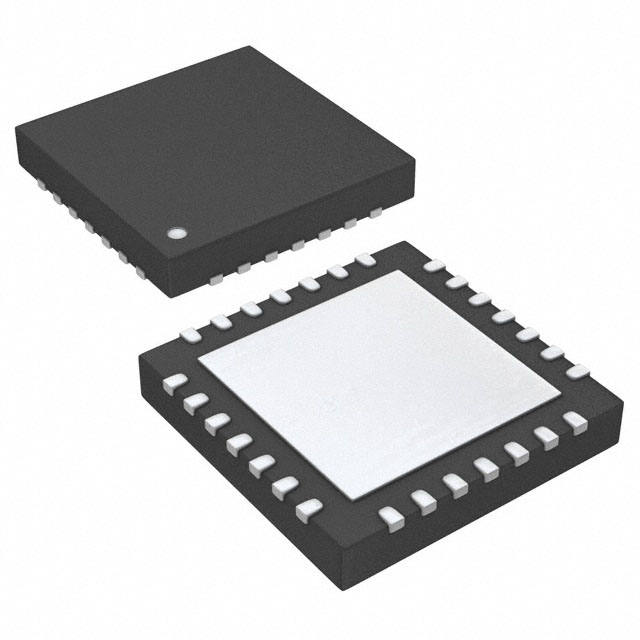
Microchip Technology MTCH650T-I/MV
- Part No.:
- MTCH650T-I/MV
- Manufacturer:
- Microchip Technology
- Category:
- Sensor and Detector Interfaces
- Package:
- 28-UFQFN Exposed Pad
- Datasheet:
-
 MTCH650T-I/MV.pdf
- Description:
- IC CONVERTER LVL SHIFTER 20UQFN
- Quantity:
- Payment:

- Shipping:

Inventory:1,764
Please send an inquiry. Send us your inquiry, and we will respond immediately.
Product details
Overview
MTCH650T-I/MV from Microchip Technology is a 21-channel high-voltage level shifter IC with serial SPI interface and independent output enable (OE), operating from 1.8V to 5.5V input and supporting external VPPIN up to 18V. It delivers up to 100 mA total output current (5 mA per channel), features <200 µA quiescent current, and targets HV display bias, capacitive touch driver, and segmented LCD/EL panel control.
For engineers reviewing the MTCH650T-I/MV datasheet, MTCH650T-I/MV pinout, MTCH650T-I/MV application, or MTCH650T-I/MV equivalent, key selection criteria include its 21 HV analog outputs, OE-independent latching, 1 MHz SPI interface, external boost voltage compatibility, and SOIC/UQFN package options - all critical for low-power, high-channel-count HV switching in space-constrained industrial and consumer displays.
Technical Context
The MTCH650T-I/MV functions as a programmable HV line driver without integrated boost circuitry - it requires an external high-voltage source connected to VPPIN (3.6–18V). Its 21 OUTxx pins are digitally controlled via a 24-bit serial interface (3-byte DATA word) and configured using a dedicated CONFIG word that sets shutdown state and soft-start behavior, though voltage/current regulation is handled externally.
Operation relies on three core digital inputs: OE (asynchronous output enable), LE (active-low latch enable), and standard SPI CLK/DIN signals. All 21 HV outputs are level-shifted analog drivers referenced to VPPIN, with each capable of sourcing up to 5 mA while maintaining rail-to-rail logic-controlled states - enabling precise per-channel HV activation in multiplexed display architectures.
Key Specifications
| Parameter | Value and Actual Design Meaning |
|---|---|
| Input Voltage Range | 1.8V to 5.5V - powers internal logic and level shifters; decoupling with ≥1 µF capacitor required at VDD. |
| VPPIN Range | 3.6V to 18V - external HV supply input; defines maximum output voltage swing across all 21 channels. |
| Output Channels | 21 HV analog outputs (OUT00–OUT20) - each independently controllable via 21-bit DATA register. |
| Max Output Current | 100 mA total (5 mA per channel) - limits simultaneous active channel count under full load conditions. |
| Quiescent Current | <200 µA - enables battery-powered operation with minimal standby power draw. |
| SPI Interface Speed | Up to 1 MHz - supports fast configuration updates without requiring high-speed MCU peripherals. |
| Shutdown Current | 1.5 µA typical - ensures ultra-low power retention during system sleep modes. |
Pinout & Package
MTCH650T-I/MV is available in 28-pin SOIC and 28-pin UQFN (4×4 mm) packages. Both variants share identical pin functionality and I/O mapping per Microchip DS40001749A.
| Pin/Terminal | Circuit Role | Design Meaning |
|---|---|---|
| VSS | Ground reference | Electrical return path for all internal circuits and HV outputs; must be low-impedance. |
| VDD | Logic supply input | Powers internal registers, SPI interface, and level-shifting circuitry; requires ≥1 µF decoupling. |
| VPPIN | External HV supply input | Provides high-voltage rail to all 21 OUTxx pins; accepts 3.6–18V; decoupling ≥1 µF mandatory. |
| OE | Asynchronous output enable | Drives all OUTxx to GND when low; enables configured outputs when high; overrides SPI timing. |
| LE | Latch enable (active-low) | Transfers serial data from shift register into output latches on rising edge; acts as chip-select when held high. |
| CLK | SPI clock input | Falling-edge sampled; synchronizes DIN data loading; max 1 MHz frequency supported. |
| DIN | SPI data input | Serial 24-bit stream: LSB = 0 selects CONFIG word, LSB = 1 selects DATA word. |
| OUT00–OUT20 | HV analog outputs | 21 individually controllable level-shifted outputs; each sources up to 5 mA when enabled by OE and DATA register. |
Key Features
| Feature | Design Value |
|---|---|
| 21-channel HV level shifting | Enables direct drive of 21 independent high-voltage nodes (e.g., EL panel segments or LCD backplanes) from low-voltage MCU logic. |
| Independent OE control | Allows instantaneous global on/off of all HV outputs without retransmitting SPI data - critical for flicker-free display blanking. |
| 24-bit serial interface | Supports both configuration (CONFIG) and output mask (DATA) loading over same 3-wire SPI bus, minimizing MCU pin count. |
| Low-power operation | Sub-200 µA quiescent and 1.5 µA shutdown currents enable integration into energy-sensitive portable and IoT display systems. |
| SOIC/UQFN dual packaging | Offers design flexibility: SOIC for prototyping and repairability; UQFN (4×4 mm) for compact, high-density PCB layouts. |
Applications
| EL Backlight Driver | Capacitive Touch Panel Controller |
|---|---|
Use Scenario: Driving electroluminescent (EL) lamp arrays in handheld medical devices requiring uniform brightness and low EMI. IC Role / Device Role / Timing Role: HV line driver providing 21 individually switched 12V outputs synchronized to PWM-modulated backlight dimming. Use Value: Eliminates need for discrete HV transistors and reduces BOM count by integrating 21 channels with OE-based global blanking for zero-flicker transitions. | Use Scenario: Controlling electrode bias sequencing in multi-layer projected capacitive touch sensors used in automotive infotainment panels. IC Role / Device Role / Timing Role: High-voltage sequencer generating precise 10–15V bias waveforms across 21 sensing electrodes under MCU SPI command. Use Value: Enables dynamic electrode reconfiguration and noise-immune AC coupling via synchronized OE gating and low-quiescent-current operation. |
| Segmented LCD Bias Generator | Industrial HMI Display Interface |
Use Scenario: Supplying segment-specific bias voltages in large-format alphanumeric LCD modules for factory floor HMIs. IC Role / Device Role / Timing Role: Programmable HV multiplexer delivering up to 18V to individual LCD segments based on 21-bit DATA register contents. Use Value: Replaces mechanical relays or discrete MOSFET arrays with single-chip solution offering faster update rates and improved reliability. | Use Scenario: Interfacing microcontroller GPIOs to high-voltage indicators, status LEDs, and alarm drivers in industrial control cabinets. IC Role / Device Role / Timing Role: Logic-level translator and current amplifier converting 3.3V/5V MCU outputs into 12–18V, 5 mA capable signals for remote panel elements. Use Value: Simplifies isolation design by consolidating 21 HV outputs with built-in latch control and OE-based fail-safe shutdown. |
Equivalent & Alternatives
The following parts are listed as comparable options for similar HV level shifter applications.
| Alternative Part | Technical Difference | Application Difference | Selection Advice |
|---|---|---|---|
| MTCH652T-I/MV | Integrated boost converter (19-channel), no VPPIN; uses OSCIN/PWM and LC pins; lower channel count. | Self-contained HV generation eliminates external supply but lacks MTCH650T-I/MV's 21-channel flexibility and external VPPIN range. | Select MTCH652T-I/MV only if board space constraints prohibit external boost and 19 channels suffice. |
| TPS65136RGTR | Dual-output HV DC-DC controller (±15V), no integrated level shifters; requires external FETs and gate drivers. | Designed for TFT-LCD source/gate drivers, not discrete HV line driving; lacks serial interface and per-channel control. | Choose TPS65136RGTR when generating symmetric bipolar HV rails is required, not for 21-channel unidirectional level shifting. |
Compared with MTCH652T-I/MV, MTCH650T-I/MV provides two additional HV outputs and full external VPPIN flexibility at the cost of requiring an external boost stage; versus TPS65136RGTR, it delivers integrated digital control and per-pin latching - making MTCH650T-I/MV uniquely suited for applications demanding high channel count, low-power, and MCU-driven HV sequencing.
Availability
MTCH650T-I/MV is available at Aetrix Electronics and suitable for EL backlighting, capacitive touch panel control, segmented LCD biasing, and industrial HMI display interfaces requiring stable component supply and long-term manufacturability.
Supply support for MTCH650T-I/MV includes scheduled delivery planning, volume procurement assistance, BOM continuity management, traceable sourcing, and lifecycle availability coordination for OEM customers, industrial embedded developers, connected-device designers, and electronics production programs.
Manufacturer
Microchip Technology Inc. is a leading provider of microcontrollers, analog components, and connectivity solutions, headquartered in Chandler, Arizona, with global design and manufacturing operations.
The MTCH650T-I/MV belongs to Microchip's MTCH650/2 family of programmable high-voltage drivers, designed specifically for low-pin-count, low-power, and high-channel-count HV interface applications in displays and human-machine interfaces.
FAQ
What is the function of the VPPIN pin on the MTCH650T-I/MV?
The VPPIN pin on the MTCH650T-I/MV serves as the external high-voltage supply input, accepting 3.6V to 18V to power all 21 HV output channels. Unlike the MTCH652, the MTCH650T-I/MV does not include an internal boost circuit - VPPIN must be driven by an external HV source such as a DC-DC converter or another MTCH652 device. A minimum 1 µF decoupling capacitor is required between VPPIN and VSS.
How many output channels does the MTCH650T-I/MV support, and what is the per-channel current limit?
The MTCH650T-I/MV supports 21 high-voltage output channels (OUT00 through OUT20), each capable of sourcing up to 5 mA. The total output current is rated at 100 mA, meaning up to 20 channels may be fully active simultaneously under worst-case conditions. This per-channel rating ensures stable operation across diverse display and sensor biasing loads without thermal derating in standard SOIC or UQFN packages.
Does the MTCH650T-I/MV include an integrated boost converter?
No, the MTCH650T-I/MV does not include an integrated boost converter. It is a pure HV level shifter and line driver that requires an external high-voltage supply connected to the VPPIN pin. In contrast, the MTCH652T-I/MV integrates a boost circuit with PWM input (OSCIN) and inductor connection (LC). The MTCH650T-I/MV's architecture allows greater flexibility in HV source selection, higher output voltage range (up to 18V), and 21-channel capability - making it ideal when external boost control or higher channel density is needed.
What is the role of the OE (Output Enable) pin on the MTCH650T-I/MV?
The OE (Output Enable) pin on the MTCH650T-I/MV provides asynchronous, hardware-level control over all 21 HV outputs. When OE is logic low, all OUTxx pins are actively driven to VSS (GND); when OE is logic high, outputs reflect the states set in the DATA register. Critically, OE operates independently of the SPI interface and latch enable (LE), enabling instant global blanking or safety shutdown - essential for flicker-free display updates and fail-safe system behavior in industrial HMIs and medical devices.
Which package options are available for the MTCH650T-I/MV, and how do they differ electrically?
The MTCH650T-I/MV is offered in two RoHS-compliant packages: 28-pin SOIC (wide-body) and 28-pin UQFN (4×4 mm, 0.5 mm pitch). Electrically, both packages share identical pinout, absolute maximum ratings, and functional specifications - including 1.8–5.5V VDD operation, 3.6–18V VPPIN support, and 21-channel HV output capability. The UQFN variant offers superior thermal performance (2W vs. 1.4W SOIC at 25°C ambient) and reduced PCB footprint, while the SOIC version simplifies prototyping, rework, and automated optical inspection.
MTCH650T-I/MV Specifications
- Product attributes
- Attribute value
- Manufacturer:
- Microchip Technology
- Package/Case:
- 28-UFQFN Exposed Pad
- Series:
- -
- Packaging:
- Tape & Reel (TR)
- Product Status:
- Active
- Programmable:
- Not Verified
- Type:
- Level Shifter
- Input Type:
- -
- Output Type:
- -
- Current - Supply:
- 200 µA
- Operating Temperature:
- -40°C ~ 85°C
- Grade:
- -
- Qualification:
- -
- Mounting Type:
- Surface Mount
- Supplier Device Package:
- 28-UQFN (4x4)
MTCH650T-I/MV FAQ
1.How can I place an order for MTCH650T-I/MV through Aetrix?
Please submit a Request for Quotation (RFQ) for MTCH650T-I/MV on Aetrix. Our sales agent will provide a competitive quotation and guide you through the order confirmation once you accept the terms.
2.Are the price and stock information for MTCH650T-I/MV reliable?
The price and inventory of MTCH650T-I/MV are updated periodically and may fluctuate due to market conditions. Stock and pricing data are typically refreshed every 24 hours. Quotation validity for MTCH650T-I/MV is usually 5 days.
3.What payment methods are accepted for MTCH650T-I/MV?
We accept Wire Transfer, PayPal, Credit Card, Western Union, MoneyGram, and Escrow for MTCH650T-I/MV transactions.
Note: Certain payment methods may incur a processing fee.
4.How is shipping managed for MTCH650T-I/MV?
MTCH650T-I/MV orders can be shipped via leading logistics carriers, including DHL, UPS, FedEx, TNT, or Registered Mail.
Once your MTCH650T-I/MV order is processed, you will receive an email with the shipment details and tracking number.
Note: Tracking information may take up to 24 hours to appear. Express delivery typically takes 3–5 business days.
5.How can I obtain technical support or documentation for MTCH650T-I/MV?
For technical support, including MTCH650T-I/MV datasheets, pinout diagrams, or application guidance, please contact our engineering support team. They can provide detailed documentation and assistance for your MTCH650T-I/MV requirements.
6.How does Aetrix verify that MTCH650T-I/MV is sourced from the original manufacturer or authorized distributors?
All MTCH650T-I/MV products on Aetrix are procured from qualified distributors and authorized channels. Our dedicated quality assurance team conducts strict verification, including traceability checks and, if necessary, third-party testing. This ensures that MTCH650T-I/MV meets industry standards.
7.What is the process for return or replacement of MTCH650T-I/MV?
All MTCH650T-I/MV units undergo pre-shipment inspection (PSI). If there is an issue with MTCH650T-I/MV, returns or replacements are accepted under the following conditions:
1.Quantity discrepancies, incorrect items, or visible external defects (such as breakage or corrosion), acknowledged by Aetrix.
2.The issue is reported within 90 days of delivery.
3.The MTCH650T-I/MV part is unused and in its original packaging.
Return procedure for MTCH650T-I/MV:
1.Submit a request within 90 days.
2.Obtain a Return Material Authorization (RMA) from Aetrix.
MTCH650T-I/MV Tags

-
RE46C100S8TF
Microchip Technology

-
XTR111AIDRCR
Texas Instruments

-
XTR111AIDGQR
Texas Instruments

-
XTR117AIDGKR
Texas Instruments
-
XTR111AIDGQT
Texas Instruments

-
XTR115UA/2K5
Texas Instruments
-
MAX14626ETT+T
Analog Devices Inc./Maxim Integrated
-
XTR116UA/2K5
Texas Instruments
-
XTR115U/2K5
Texas Instruments
-
XTR116U/2K5
Texas Instruments

-
PGA308AIDGSR
Texas Instruments
-
XTR300AIRGWR
Texas Instruments
Tech Hub

TTL and CMOS logic families differ in thresholds, loading, output drive, power and timing. This engineering guide compares 74HC and 74HCT, calculates noise margins and checks 3.3 V/5 V compatibility.

A practical engineering guide to 3.3V and 5V logic compatibility, input thresholds, resistor dividers, translator ICs, MOSFET level shifting, I2C pull-ups, timing limits and power-sequencing risks.

The 74HC595 uses push-pull logic outputs, while the TPIC6B595 uses 50 V open-drain DMOS sinks for higher-power loads. This guide compares timing, current limits, 3.3 V interfacing, load wiring, thermal…

The 74HC595 converts serial data into eight stable parallel outputs. This guide covers pin functions, shift and storage timing, OE and MR behavior, drive-current limits, cascading, voltage compatibilit…

A technical comparison of level-sensitive latches and edge-triggered flip-flops, covering timing windows, setup and hold limits, master–slave operation, time borrowing, race-through, HDL inference and…

A D latch stores one bit while Enable controls when data can pass. This reference covers gate-level operation, truth tables, transparency, setup and hold timing, LE versus OE, common ICs and practical …

An SR latch stores one bit through cross-coupled feedback. This engineering reference covers NOR and NAND implementations, truth tables, forbidden-state recovery, gated operation, switch debouncing, fa…

Latch circuits retain one bit through feedback. This technical reference covers SR and D latches, truth tables, transparency, timing limits, latch-versus-flip-flop behavior, applications and common log…

An engineering guide to LED driver operation, constant-current and constant-voltage outputs, linear and switching topologies, dimming, IC selection, calculations, replacement compatibility, and fault c…

Operational amplifier guide covering op amp basics, feedback, ideal vs real op amps, common configurations, buffer circuits, offset, bias current, gain-bandwidth, slew rate, rail-to-rail limits and sel…


