
 My Inquiry
 My Account


onsemi NC7SP38P5X
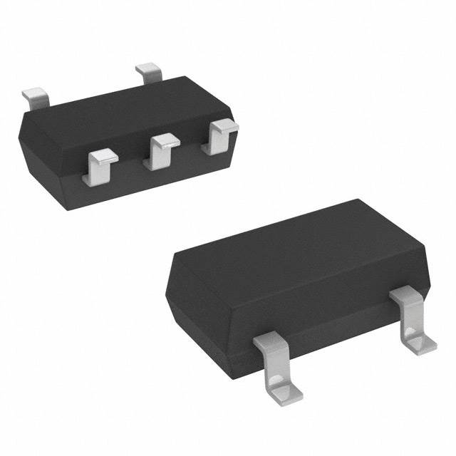
- Part No.:
- NC7SP38P5X
- Manufacturer:
- onsemi
- Category:
- Gates and Inverters
- Package:
- 5-TSSOP, SC-70-5, SOT-353
- Datasheet:
-
 NC7SP38P5X.pdf
- Description:
- IC GATE NAND 1CH 2-INP SC70-5
- Quantity:
- Payment:

- Shipping:

Inventory:33,908
Please send an inquiry. Send us your inquiry, and we will respond immediately.
Product details
Overview
NC7SP38P5X from onsemi is a single 2-input NAND gate with open-drain output, designed for ultra-low-power logic in space-constrained applications. It operates across 0.9 V to 3.6 V supply, delivers 2.9 ns propagation delay at 3.3 V (typ), supports input/output over-voltage tolerance up to 3.6 V, and features IOFF partial power-down protection-used in battery-powered sensor interface and level-shifting circuits.
For engineers reviewing the NC7SP38P5X datasheet, pinout, applications, or equivalent options, this page provides verified electrical specs, SC-88A package details, functional truth table behavior, IOFF-enabled power gating capability, and validated alternatives for low-voltage logic design.
Technical Context
The NC7SP38P5X implements standard 2-input NAND logic with open-drain output architecture, requiring an external pull-up resistor for high-level assertion. Its IOFF circuitry disables input and output leakage paths when VCC = 0 V, enabling live insertion and partial power-down system operation.
It supports rail-to-rail input voltage range (0–3.6 V) independent of VCC, allowing mixed-voltage interfacing between 1.2 V, 1.8 V, 2.5 V, and 3.3 V domains. Propagation delay scales inversely with VCC, ranging from 32.4 ns at 0.9 V to 2.9 ns at 3.3 V under 10 pF load.
Key Specifications
| Parameter | Value and Actual Design Meaning |
|---|---|
| VCC Range | 0.9 V to 3.6 V - enables direct integration into sub-1V IoT nodes and multi-rail systems without level shifters |
| tPD (Typ) | 2.9 ns at 3.3 V, 10 pF - supports >100 MHz toggle rates in low-power clocked logic paths |
| IOFF Leakage | ≤0.5 µA at VCC = 0 V - prevents back-powering of powered-down sections during hot-swap or sleep modes |
| Input Tolerance | Up to 3.6 V regardless of VCC - allows safe interfacing with higher-voltage controllers or sensors |
| IOL Drive | 2.6 mA at 3.3 V - sufficient to drive standard CMOS inputs or small LED indicators via pull-up |
| CIN / COUT | 2.0 pF / 4.0 pF - minimizes capacitive loading on driving gates and reduces dynamic power in dense layouts |
Pinout & Package
NC7SP38P5X is packaged in SC-88A (SOT-353), a 5-pin, 1.45 mm × 1.0 mm surface-mount package with exposed pad option not present; pin 1 marked by dot, pin count and orientation confirmed per onsemi case 419A-02.
| Pin/Terminal | Circuit Role | Design Meaning |
|---|---|---|
| 1 (A) | First input | Accepts logic signal; tolerant to 3.6 V regardless of VCC value |
| 2 (B) | Second input | Accepts logic signal; identical voltage tolerance and leakage as Pin 1 |
| 3 (GND) | Ground reference | Return path for supply and signal currents; must be low-impedance for noise immunity |
| 4 (Y) | Open-drain output | Sinks current only; requires external pull-up to define HIGH state voltage level |
| 5 (VCC) | Positive supply | Power rail for internal logic; IOFF activation occurs when VCC = 0 V |
Key Features
| Feature | Design Value |
|---|---|
| Ultra-low VCC operation | Functional down to 0.9 V - supports energy harvesting and coin-cell-powered devices |
| IOFF partial power-down | Blocks I/O leakage when VCC = 0 V - essential for hot-plug and multi-domain power sequencing |
| Over-voltage tolerant I/O | Inputs/outputs withstand 3.6 V even at VCC = 0.9 V - eliminates need for external clamping diodes |
| Low dynamic power | CPD = 6.0 pF - reduces switching power consumption in high-frequency enable/control signals |
Applications
| IoT Sensor Node Interface | Multi-Rail Level Shifter |
|---|---|
Use Scenario: Interfacing 3.3 V microcontroller GPIO to 1.8 V environmental sensor interrupt line. IC Role / Device Role / Timing Role: NAND gate configured as active-low enable with open-drain output pulls sensor's OD interrupt low while tolerating 3.3 V MCU side. Use Value: Eliminates discrete MOSFET level shifter; IOFF prevents back-current when sensor domain powers down independently. | Use Scenario: Translating 1.2 V FPGA configuration status signal to 2.5 V PMIC enable input. IC Role / Device Role / Timing Role: Logic gate used as bidirectional voltage translator via pull-up on Y, leveraging input over-voltage tolerance. Use Value: Supports asymmetric rail translation without direction control pins; <10 ns delay preserves timing margin in boot sequences. |
| Battery-Powered Wearable Reset Generator | Low-Power System Enable Controller |
Use Scenario: Combining low-battery detector and manual reset button to generate clean system reset pulse. IC Role / Device Role / Timing Role: NAND gate forms wired-OR reset logic with open-drain output tied to shared reset bus. Use Value: Sub-1 µA quiescent current extends battery life; 0.9 V operation ensures functionality until battery reaches end-of-life. | Use Scenario: Enabling subsystem power rails only when host processor and thermal monitor both assert readiness. IC Role / Device Role / Timing Role: NAND gate acts as dual-input enable gate with open-drain output driving enable pin of DC-DC converter. Use Value: IOFF blocks leakage during host sleep mode; 2.6 mA sink current directly drives most enable inputs without buffer stage. |
Equivalent & Alternatives
The following parts are listed as comparable options for similar NAND gate with open-drain output applications.
| Alternative Part | Technical Difference | Application Difference | Selection Advice |
|---|---|---|---|
| NC7SZ38P5X | Same SC-88A package, but push-pull output (not open-drain); no IOFF feature | Requires external pull-up for wired-OR; unsuitable for partial power-down scenarios | Select when active-HIGH output and lower output impedance are preferred over IOFF capability |
| SN74LVC1G00DBVR | Push-pull output, 1.65–5.5 V VCC range, no over-voltage tolerance beyond VCC | Cannot interface 3.6 V signals at VCC = 1.8 V; lacks IOFF for zero-VCC isolation | Choose for wider VCC range and higher drive strength where rail-matching is guaranteed |
Compared with NC7SP38P5X, NC7SZ38P5X offers faster propagation delay but forfeits open-drain flexibility and IOFF; SN74LVC1G00DBVR supports higher VCC but requires strict voltage alignment and adds layout complexity for wired-OR implementation.
Availability
NC7SP38P5X is available at Aetrix Electronics and suitable for IoT sensor interfaces, multi-rail level shifting, battery-powered wearable reset generation, low-power system enable control, and portable medical device logic conditioning requiring stable component supply and long-term lifecycle support.
Supply support for NC7SP38P5X includes scheduled delivery planning, volume procurement assistance, BOM continuity management, traceable sourcing, and lifecycle availability coordination for OEM customers, industrial embedded developers, connected-device designers, and electronics production programs.
Manufacturer
onsemi (formerly ON Semiconductor) is a global semiconductor supplier focused on energy-efficient electronics for automotive, industrial, cloud, and intelligent edge applications.
The TinyLogic ULP-A family-including NC7SP38P5X-is designed for ultra-low-power, small-footprint logic in battery-operated and space-constrained systems where supply voltage scalability and IOFF-enabled power domain isolation are critical.
FAQ
What is the maximum input voltage allowed on NC7SP38P5X pins when VCC = 1.2 V?
The NC7SP38P5X supports input voltages up to 3.6 V regardless of VCC level. When VCC = 1.2 V, pins A, B, and Y tolerate 0–3.6 V, enabling safe interfacing with higher-voltage peripherals without external protection. This over-voltage tolerance is explicitly specified in the Absolute Maximum Ratings and Recommended Operating Conditions tables of the official NC7SP38P5X datasheet.
Does NC7SP38P5X support true tri-state operation?
No, NC7SP38P5X does not provide tri-state (high-impedance) control via an enable pin. Its output is open-drain only: it actively pulls low or floats high (requiring external pull-up). The "Z" in the function table denotes high-impedance float-not controllable tri-state. For enable-controlled tri-state logic, consider dedicated bus switches or 3-state buffers instead of NC7SP38P5X.
Can NC7SP38P5X be used as a level shifter between 1.8 V and 3.3 V domains?
Yes, NC7SP38P5X can serve as a unidirectional level shifter from 1.8 V to 3.3 V. Configure the 1.8 V domain as inputs (A/B), tie the open-drain output (Y) to a 3.3 V pull-up, and use the output as a 3.3 V–compatible signal. Input over-voltage tolerance and IOFF ensure robustness during domain power sequencing-verified in NC7SP38P5X application notes for mixed-voltage interfacing.
What is the minimum supply voltage at which NC7SP38P5X guarantees correct logic operation?
The NC7SP38P5X guarantees functional operation down to 0.9 V VCC, as defined in the Recommended Operating Conditions table. At 0.9 V, propagation delay increases to 32.4 ns (typ) with 10 pF load, and VIH/VIL thresholds scale proportionally. All DC and AC specifications in the NC7SP38P5X datasheet are validated across 0.9–3.6 V, making it suitable for ultra-low-voltage energy-harvesting designs.
Is NC7SP38P5X RoHS compliant and lead-free?
Yes, NC7SP38P5X is RoHS compliant, Pb-free, halogen-free, and BFR-free, as confirmed in the Features section and Ordering Information table of the official NC7SP38P5X datasheet. The "X" suffix in the part number denotes lead-free packaging, and the SC-88A package meets JEDEC MSL Level 1 moisture sensitivity requirements for standard assembly processes.
NC7SP38P5X Specifications
- Product attributes
- Attribute value
- Manufacturer:
- onsemi
- Series:
- 7SP
- Package/Case:
- 5-TSSOP, SC-70-5, SOT-353
- Packaging:
- Tape & Reel (TR)
- Product Status:
- Obsolete
- Logic Type:
- NAND Gate
- Number of Circuits:
- 1
- Number of Inputs:
- 2
- Features:
- Open Drain
- Voltage - Supply:
- 0.9V ~ 3.6V
- Current - Quiescent (Max):
- 900 nA
- Current - Output High, Low:
- -, 2.6mA
- Input Logic Level - Low:
- 0.7V ~ 0.9V
- Input Logic Level - High:
- 1.6V ~ 2.1V
- Max Propagation Delay @ V, Max CL:
- 10ns @ 3.3V, 30pF
- Operating Temperature:
- -40°C ~ 85°C
- Grade:
- -
- Qualification:
- -
- Mounting Type:
- Surface Mount
- Supplier Device Package:
- SC-70-5
NC7SP38P5X FAQ
1.How can I place an order for NC7SP38P5X through Aetrix?
Please submit a Request for Quotation (RFQ) for NC7SP38P5X on Aetrix. Our sales agent will provide a competitive quotation and guide you through the order confirmation once you accept the terms.
2.Are the price and stock information for NC7SP38P5X reliable?
The price and inventory of NC7SP38P5X are updated periodically and may fluctuate due to market conditions. Stock and pricing data are typically refreshed every 24 hours. Quotation validity for NC7SP38P5X is usually 5 days.
3.What payment methods are accepted for NC7SP38P5X?
We accept Wire Transfer, PayPal, Credit Card, Western Union, MoneyGram, and Escrow for NC7SP38P5X transactions.
Note: Certain payment methods may incur a processing fee.
4.How is shipping managed for NC7SP38P5X?
NC7SP38P5X orders can be shipped via leading logistics carriers, including DHL, UPS, FedEx, TNT, or Registered Mail.
Once your NC7SP38P5X order is processed, you will receive an email with the shipment details and tracking number.
Note: Tracking information may take up to 24 hours to appear. Express delivery typically takes 3–5 business days.
5.How can I obtain technical support or documentation for NC7SP38P5X?
For technical support, including NC7SP38P5X datasheets, pinout diagrams, or application guidance, please contact our engineering support team. They can provide detailed documentation and assistance for your NC7SP38P5X requirements.
6.How does Aetrix verify that NC7SP38P5X is sourced from the original manufacturer or authorized distributors?
All NC7SP38P5X products on Aetrix are procured from qualified distributors and authorized channels. Our dedicated quality assurance team conducts strict verification, including traceability checks and, if necessary, third-party testing. This ensures that NC7SP38P5X meets industry standards.
7.What is the process for return or replacement of NC7SP38P5X?
All NC7SP38P5X units undergo pre-shipment inspection (PSI). If there is an issue with NC7SP38P5X, returns or replacements are accepted under the following conditions:
1.Quantity discrepancies, incorrect items, or visible external defects (such as breakage or corrosion), acknowledged by Aetrix.
2.The issue is reported within 90 days of delivery.
3.The NC7SP38P5X part is unused and in its original packaging.
Return procedure for NC7SP38P5X:
1.Submit a request within 90 days.
2.Obtain a Return Material Authorization (RMA) from Aetrix.
NC7SP38P5X Tags

-
SN74LVC1G14DBVR
Texas Instruments

-
SN74LVC1G14DCKR
Texas Instruments
-
SN74AHC1G14DBVR
Texas Instruments
-
SN74LVC1G08DBVR
Texas Instruments
-
SN74LVC1G08DCKR
Texas Instruments
-
SN74LVC1G32DCKR
Texas Instruments
-
SN74LVC1G04DBVR
Texas Instruments
.jpg)
-
74LVC1G08GW,125
Nexperia USA Inc.
-
SN74LVC1G04DCKR
Texas Instruments
-
SN74AHC1G08DBVR
Texas Instruments
-
SN74LVC1G32DBVR
Texas Instruments
-
SN74AHCT1G08DBVR
Texas Instruments
Tech Hub

Counterfeit components can hide behind convincing markings and passing basic function tests. This engineering reference covers source traceability, external inspection, X-ray, XRF, electrical testing, …

A practical engineering and sourcing framework covering lifecycle verification, lifetime-buy calculations, replacement qualification, supplier checks and counterfeit-risk controls.

TTL and CMOS logic families differ in thresholds, loading, output drive, power and timing. This engineering guide compares 74HC and 74HCT, calculates noise margins and checks 3.3 V/5 V compatibility.

A practical engineering guide to 3.3V and 5V logic compatibility, input thresholds, resistor dividers, translator ICs, MOSFET level shifting, I2C pull-ups, timing limits and power-sequencing risks.

The 74HC595 uses push-pull logic outputs, while the TPIC6B595 uses 50 V open-drain DMOS sinks for higher-power loads. This guide compares timing, current limits, 3.3 V interfacing, load wiring, thermal…

The 74HC595 converts serial data into eight stable parallel outputs. This guide covers pin functions, shift and storage timing, OE and MR behavior, drive-current limits, cascading, voltage compatibilit…

A technical comparison of level-sensitive latches and edge-triggered flip-flops, covering timing windows, setup and hold limits, master–slave operation, time borrowing, race-through, HDL inference and…

A D latch stores one bit while Enable controls when data can pass. This reference covers gate-level operation, truth tables, transparency, setup and hold timing, LE versus OE, common ICs and practical …

An SR latch stores one bit through cross-coupled feedback. This engineering reference covers NOR and NAND implementations, truth tables, forbidden-state recovery, gated operation, switch debouncing, fa…

Latch circuits retain one bit through feedback. This technical reference covers SR and D latches, truth tables, transparency, timing limits, latch-versus-flip-flop behavior, applications and common log…


