
 My Inquiry
 My Account


onsemi NCP1500DMR2G
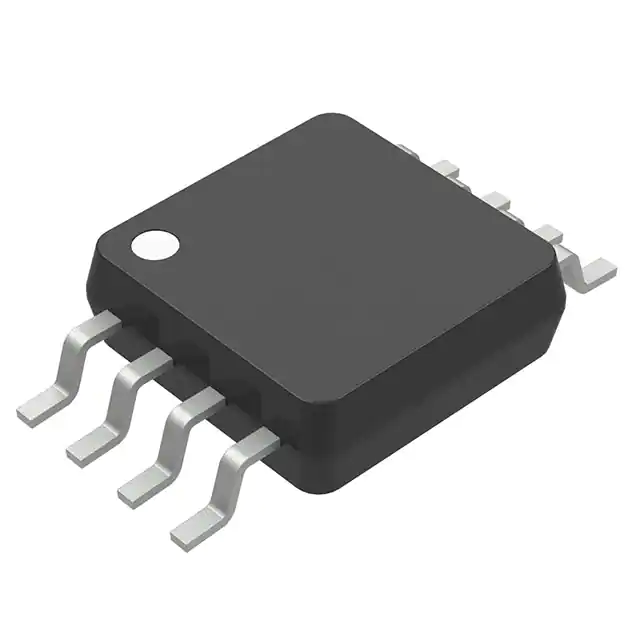
- Part No.:
- NCP1500DMR2G
- Manufacturer:
- onsemi
- Category:
- Voltage Regulators - Linear + Switching
- Package:
- 8-TSSOP, 8-MSOP (0.118", 3.00mm Width)
- Datasheet:
-
 NCP1500DMR2G.pdf
- Description:
- IC REG SGL BUCK/LINEAR MICRO8
- Quantity:
- Payment:

- Shipping:

Inventory:1,518
Please send an inquiry. Send us your inquiry, and we will respond immediately.
Product details
Overview
NCP1500DMR2G from onsemi is a dual-mode PWM/linear buck converter IC designed for baseband power regulation in portable electronics. It operates as a current-mode PWM buck regulator (270–630 kHz sync frequency) or low-noise linear regulator, automatically transitioning based on presence of an external synchronization signal at the SYN pin. Digitally programmable output voltages (1.0 V, 1.3 V, 1.5 V, 1.8 V) and internal thermal shutdown with hysteresis support battery-powered handset supply applications.
For engineers reviewing the NCP1500DMR2G datasheet, pinout, applications, or equivalent options, key selection criteria include mode-switching behavior, digitally selectable output voltage, Micro8 package footprint, 2.7–5.4 V input range, and 0.18 µA shutdown current - all critical for low-power portable system design.
Technical Context
The NCP1500DMR2G integrates two independent regulation paths: a current-mode PWM controller with cycle-by-cycle current limiting and built-in slope compensation for stable >50% duty cycles, and a linear regulator path activated when the SYN pin is pulled low or left floating for ~6 seconds. Mode selection is hardware-driven and non-software-configurable.
Its error amplifier feeds both regulation paths; in PWM mode, its output passes through a subtraction circuit during overcurrent events to reduce duty cycle, while in linear mode it directly controls the pass element. Output voltage is set via binary-encoded CB0/CB1 pins selecting internal resistor-divider ratios referenced to a 0.8 V internal bandgap.
Key Specifications
| Parameter | Value and Actual Design Meaning |
|---|---|
| Input Voltage Range | 2.7 V to 5.4 V - supports single-cell Li-ion and multi-cell alkaline battery inputs without pre-regulation. |
| Output Voltage Options | 1.0 V / 1.3 V / 1.5 V / 1.8 V - selected by CB0/CB1 logic levels; internally pulled low defaults to 1.5 V. |
| PWM Sync Frequency | 270 kHz to 630 kHz - externally synchronized; enables EMI control and avoids noise-sensitive bands. |
| Shutdown Current | 0.18 µA typical - enables ultra-low quiescent power during system sleep states. |
| Thermal Shutdown Threshold | 150°C with 25°C hysteresis - protects die under sustained overload or poor PCB thermal design. |
| Max Output Current (PWM) | 800 mA peak switch current - supports moderate baseband loads with external 15 µH inductor. |
| Linear Mode Output Current | 50 mA nominal, 100 mA transient - sufficient for biasing idle baseband circuits with low noise. |
Pinout & Package
Package: Micro8 (MSOP-8), Pb-free, 3.0 mm × 3.0 mm body, 0.65 mm pitch, 1.10 mm max height (Case 846A-02).
| Pin/Terminal | Circuit Role | Design Meaning |
|---|---|---|
| 1 - SHD | Shutdown control input | Drives device into 0.18 µA standby when pulled low; requires external pull-up for normal operation. |
| 2 - SYN | Sync clock input | Presence ≥1.3 V triggers PWM mode; absence for ~6 s forces linear mode; must be pulled low (not open) to ensure full disable. |
| 3 - VO | Feedback node | Connects to internal resistive divider; sets output voltage via CB0/CB1; no external resistor required. |
| 4 - LX | Switch node | Drain of internal P-MOSFET; connects to external inductor and Schottky diode (e.g., MBRM120). |
| 5 - VIN | Main power input | 2.7–5.4 V supply; requires 10 µF ceramic bypass capacitor placed near pin. |
| 6 - GND | Power ground | Common return for VIN, LX, and internal circuits; must be low-impedance connection to minimize noise coupling. |
| 7 - CB1 | Voltage select bit 1 | Binary input (H/L) selecting one of four output voltages; internally pulled low - open = L. |
| 8 - CB0 | Voltage select bit 0 | Binary input (H/L) completing 2-bit code; truth table defines 1.0/1.3/1.5/1.8 V outputs. |
Key Features
| Feature | Design Value |
|---|---|
| Dual-mode automatic transition | Seamlessly switches between high-efficiency PWM and low-noise linear regulation based solely on SYN pin state - no firmware or external logic needed. |
| Digitally programmable output | Four precise output voltages (1.0/1.3/1.5/1.8 V) set via two logic-level pins - eliminates external feedback resistors and simplifies BOM. |
| Current-mode PWM control | Enables fast transient response and inherent cycle-by-cycle current limiting up to 800 mA - improves reliability under short-circuit conditions. |
| Integrated slope compensation | Stabilizes current-mode operation above 50% duty cycle - prevents subharmonic oscillation without external components. |
| Thermal shutdown with hysteresis | Shuts down at 150°C and re-enables only after die cools to ≤125°C - prevents thermal runaway and allows safe recovery without system reset. |
Applications
| Baseband Power Supply | DSP Core Supply |
|---|---|
Use Scenario: Regulating power to GSM/CDMA baseband processors during active call and standby modes. IC Role / Device Role / Timing Role: Dual-mode buck converter providing efficient PWM power during transmission bursts and ultra-low-noise linear bias during receive/idle periods. Use Value: Extends battery life by switching to 0.18 µA shutdown or low-IQ linear mode when baseband is inactive, while maintaining clean supply for sensitive analog sections. | Use Scenario: Delivering stable, low-noise voltage to digital signal processor cores in PDAs and handheld media players. IC Role / Device Role / Timing Role: Programmable-output regulator adapting to DSP core voltage requirements (1.3 V or 1.5 V) and load dynamics across processing states. Use Value: Eliminates need for multiple fixed-output LDOs; single NCP1500DMR2G supports multiple voltage configurations via CB0/CB1 pins. |
| Portable Handset RF Front-End Bias | Low-Power Sensor Hub Supply |
Use Scenario: Supplying bias voltage to RF transceiver analog front-end blocks requiring minimal switching noise. IC Role / Device Role / Timing Role: Linear regulator mode provides <100 µVpp output ripple - critical for preserving RF receiver sensitivity and SNR. Use Value: Avoids EMI from switching regulators near RF sections; enables co-location of power IC and RF IC on compact PCBs. | Use Scenario: Powering always-on inertial or environmental sensors in wearables and IoT edge nodes. IC Role / Device Role / Timing Role: Ultra-low-quiescent regulator delivering 1.8 V at <50 mA with 0.18 µA shutdown - minimizes average current draw in sleep-dominated operation. Use Value: Enables multi-week battery life in coin-cell-powered sensor hubs by eliminating wake-up overhead from external enable sequencing. |
Equivalent & Alternatives
The following parts are listed as comparable options for similar dual-mode buck regulator applications.
| Alternative Part | Technical Difference | Application Difference | Selection Advice |
|---|---|---|---|
| TPS62260DRVR | Single-mode synchronous buck only; no linear mode; higher 2.25 MHz fixed frequency; lower 17 µA quiescent current in PWM. | Lacks automatic noise-aware mode switching; requires external LDO for low-noise bias; better suited for space-constrained, high-efficiency-only designs. | Select TPS62260DRVR when board area is critical and system noise budget allows pure switching operation with post-regulation filtering. |
| MAX8640YETA+ | Dual-output buck + LDO combo; fixed 1.2 V/1.8 V outputs; no digital voltage selection; includes I2C interface for dynamic voltage scaling. | Provides dedicated low-noise LDO path but lacks auto-transition logic; requires host MCU coordination for mode changes. | Select MAX8640YETA+ when multiple regulated rails and software-controlled voltage scaling are required, and linear mode must be explicitly commanded. |
Compared with TPS62260DRVR and MAX8640YETA+, the NCP1500DMR2G uniquely delivers autonomous PWM/linear mode switching without MCU intervention or additional ICs - reducing system complexity and firmware dependencies in battery-sensitive portable platforms.
Availability
NCP1500DMR2G is available at Aetrix Electronics and suitable for portable handset baseband supplies, PDA power management, and DSP circuitry requiring stable component supply with long-term lifecycle assurance.
Supply support for NCP1500DMR2G includes scheduled delivery planning, volume procurement assistance, BOM continuity management, traceable sourcing, and lifecycle availability coordination for OEM customers, industrial embedded developers, connected-device designers, and electronics production programs.
Manufacturer
onsemi (formerly ON Semiconductor) is a global semiconductor supplier specializing in energy-efficient power management, analog, sensing, and connectivity solutions for automotive, industrial, cloud, and portable markets.
The NCP1500DMR2G belongs to onsemi's portable power management product line, engineered specifically for battery-powered communication devices where adaptive efficiency/noise trade-offs are essential to maximize runtime and signal integrity.
FAQ
What is the function of the SYN pin on the NCP1500DMR2G?
The SYN pin on the NCP1500DMR2G serves as the external synchronization input that determines operating mode: a valid clock signal (≥1.3 V, 270–630 kHz, 20–80% duty cycle) forces PWM mode, while absence for ~6 seconds or being pulled low activates linear regulator mode. It is not a general-purpose GPIO and must be actively driven low - not left floating - to ensure full linear-mode operation and lowest quiescent current.
How does the NCP1500DMR2G select its output voltage?
The NCP1500DMR2G selects output voltage using two digital inputs - CB0 and CB1 - which form a 2-bit code referencing internal resistor-divider networks tied to a 0.8 V reference. Valid combinations yield 1.0 V (CB0=H, CB1=H), 1.3 V (CB0=L, CB1=H), 1.5 V (CB0=L, CB1=L), or 1.8 V (CB0=H, CB1=L). Both pins are internally pulled low, so leaving them unconnected defaults to 1.5 V without external components.
Does the NCP1500DMR2G require external compensation components?
No, the NCP1500DMR2G does not require external compensation components. Its error amplifier is fully compensated internally for both PWM and linear modes, enabling stable operation with only the recommended 10 µF input and output ceramic capacitors and a 15 µH inductor. This eliminates tuning effort and reduces bill-of-materials cost compared to open-loop or externally compensated regulators.
What protection features are integrated into the NCP1500DMR2G?
The NCP1500DMR2G integrates thermal shutdown with 25°C hysteresis (trips at 150°C), cycle-by-cycle current limiting in PWM mode (800 mA peak), and overvoltage protection that forces PFM/skip mode if output exceeds programmed voltage by >5%. It also includes ESD protection rated to 2.0 kV HBM and latch-up immunity per JESD78 (150 mA), ensuring robustness in handheld assembly and field use.
Can the NCP1500DMR2G operate without an external inductor?
No, the NCP1500DMR2G cannot operate without an external inductor in either mode. In PWM mode, the inductor stores energy during LX conduction and delivers it to the load during off-time. In linear mode, the inductor remains in series with the output path and is used by the internal bypass transistor to manage stored energy and prevent oscillation - as described in the patent-pending linear-mode architecture. Omitting the inductor will result in malfunction or damage.
NCP1500DMR2G Specifications
- Product attributes
- Attribute value
- Manufacturer:
- onsemi
- Series:
- -
- Package/Case:
- 8-TSSOP, 8-MSOP (0.118", 3.00mm Width)
- Packaging:
- Tape & Reel (TR)
- Product Status:
- Obsolete
- Topology:
- Step-Down (Buck) (1), Linear (LDO) (1)
- Number of Outputs:
- 1
- Frequency - Switching:
- 270kHz ~ 639kHz
- Voltage/Current - Output 1:
- 1V, 1.3V, 1.5V, 1.8V, -
- Voltage/Current - Output 2:
- -
- Voltage/Current - Output 3:
- -
- w/LED Driver:
- No
- w/Supervisor:
- No
- w/Sequencer:
- No
- Voltage - Supply:
- 2.7V ~ 5.4V
- Operating Temperature:
- -40°C ~ 85°C
- Grade:
- -
- Qualification:
- -
- Mounting Type:
- Surface Mount
- Supplier Device Package:
- 8-MSOP
NCP1500DMR2G FAQ
1.How can I place an order for NCP1500DMR2G through Aetrix?
Please submit a Request for Quotation (RFQ) for NCP1500DMR2G on Aetrix. Our sales agent will provide a competitive quotation and guide you through the order confirmation once you accept the terms.
2.Are the price and stock information for NCP1500DMR2G reliable?
The price and inventory of NCP1500DMR2G are updated periodically and may fluctuate due to market conditions. Stock and pricing data are typically refreshed every 24 hours. Quotation validity for NCP1500DMR2G is usually 5 days.
3.What payment methods are accepted for NCP1500DMR2G?
We accept Wire Transfer, PayPal, Credit Card, Western Union, MoneyGram, and Escrow for NCP1500DMR2G transactions.
Note: Certain payment methods may incur a processing fee.
4.How is shipping managed for NCP1500DMR2G?
NCP1500DMR2G orders can be shipped via leading logistics carriers, including DHL, UPS, FedEx, TNT, or Registered Mail.
Once your NCP1500DMR2G order is processed, you will receive an email with the shipment details and tracking number.
Note: Tracking information may take up to 24 hours to appear. Express delivery typically takes 3–5 business days.
5.How can I obtain technical support or documentation for NCP1500DMR2G?
For technical support, including NCP1500DMR2G datasheets, pinout diagrams, or application guidance, please contact our engineering support team. They can provide detailed documentation and assistance for your NCP1500DMR2G requirements.
6.How does Aetrix verify that NCP1500DMR2G is sourced from the original manufacturer or authorized distributors?
All NCP1500DMR2G products on Aetrix are procured from qualified distributors and authorized channels. Our dedicated quality assurance team conducts strict verification, including traceability checks and, if necessary, third-party testing. This ensures that NCP1500DMR2G meets industry standards.
7.What is the process for return or replacement of NCP1500DMR2G?
All NCP1500DMR2G units undergo pre-shipment inspection (PSI). If there is an issue with NCP1500DMR2G, returns or replacements are accepted under the following conditions:
1.Quantity discrepancies, incorrect items, or visible external defects (such as breakage or corrosion), acknowledged by Aetrix.
2.The issue is reported within 90 days of delivery.
3.The NCP1500DMR2G part is unused and in its original packaging.
Return procedure for NCP1500DMR2G:
1.Submit a request within 90 days.
2.Obtain a Return Material Authorization (RMA) from Aetrix.
NCP1500DMR2G Tags

-
TPS6521905RHBR
Texas Instruments
-
MIC3385YHL-TR
Microchip Technology
-
A4402ELPTR-T
Allegro MicroSystems

-
LM26480SQ-AA/NOPB
Texas Instruments
-
A4402KLPTR-T
Allegro MicroSystems
-
BD71847AMWV-E2
ROHM Semiconductor
-
ADP5040ACPZ-1-R7
Analog Devices Inc.
-
LT3048IDC#TRPBF
Analog Devices Inc.
-
ADP5037ACPZ-R7
Analog Devices Inc.

-
XRP7714ILB-F
MaxLinear, Inc.
-
LTC3260EDE#TRPBF
Analog Devices Inc.
-
LTC3260EMSE#PBF
Analog Devices Inc.
Tech Hub

Counterfeit components can hide behind convincing markings and passing basic function tests. This engineering reference covers source traceability, external inspection, X-ray, XRF, electrical testing, …

A practical engineering and sourcing framework covering lifecycle verification, lifetime-buy calculations, replacement qualification, supplier checks and counterfeit-risk controls.

TTL and CMOS logic families differ in thresholds, loading, output drive, power and timing. This engineering guide compares 74HC and 74HCT, calculates noise margins and checks 3.3 V/5 V compatibility.

A practical engineering guide to 3.3V and 5V logic compatibility, input thresholds, resistor dividers, translator ICs, MOSFET level shifting, I2C pull-ups, timing limits and power-sequencing risks.

The 74HC595 uses push-pull logic outputs, while the TPIC6B595 uses 50 V open-drain DMOS sinks for higher-power loads. This guide compares timing, current limits, 3.3 V interfacing, load wiring, thermal…

The 74HC595 converts serial data into eight stable parallel outputs. This guide covers pin functions, shift and storage timing, OE and MR behavior, drive-current limits, cascading, voltage compatibilit…

A technical comparison of level-sensitive latches and edge-triggered flip-flops, covering timing windows, setup and hold limits, master–slave operation, time borrowing, race-through, HDL inference and…

A D latch stores one bit while Enable controls when data can pass. This reference covers gate-level operation, truth tables, transparency, setup and hold timing, LE versus OE, common ICs and practical …

An SR latch stores one bit through cross-coupled feedback. This engineering reference covers NOR and NAND implementations, truth tables, forbidden-state recovery, gated operation, switch debouncing, fa…

Latch circuits retain one bit through feedback. This technical reference covers SR and D latches, truth tables, transparency, timing limits, latch-versus-flip-flop behavior, applications and common log…


