
 My Inquiry
 My Account


onsemi NCP360MUTXG
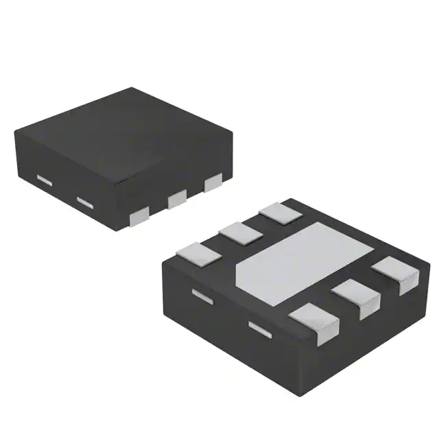
- Part No.:
- NCP360MUTXG
- Manufacturer:
- onsemi
- Category:
- Mixed Technology
- Package:
- 6-UDFN Exposed Pad
- Datasheet:
-
 NCP360MUTXG.pdf
- Description:
- TVS DEVICE MIXED 7.4V 6-UDFN
- Quantity:
- Payment:

- Shipping:

Inventory:9,479
Please send an inquiry. Send us your inquiry, and we will respond immediately.
Product details
Overview
NCP360MUTXG from onsemi is a USB-positive overvoltage protection controller with integrated PMOS FET, 5.675 V typical OVLO threshold, 3.0 V typical UVLO threshold, and open-drain FLAG output for fault indication - designed to protect downstream USB peripherals from VBUS overvoltage up to +20 V in mobile phone and portable device power paths.
For engineers reviewing the NCP360MUTXG datasheet, pinout, applications, or equivalent options, this page delivers verified package mapping (UDFN6, 2×2 mm), confirmed electrical thresholds, thermal shutdown behavior, ESD immunity (15 kV air), and real-world timing values including 0.8–1.5 µs output turn-off time and 1.0–2.0 µs alert delay.
Technical Context
The NCP360MUTXG implements dual voltage monitoring: UVLO activates below 2.85–3.15 V (50–90 mV hysteresis) to prevent operation during insufficient input, while OVLO triggers above 5.43–5.90 V (50–125 mV hysteresis) to disconnect the output within sub-microsecond response. Its internal PMOS FET provides 600 mA continuous current capability with 105–200 mV dropout at 500 mA.
FLAG is an open-drain output that pulls low upon OVLO detection and requires an external pull-up resistor; EN is an active-low enable input that forces output disconnection when high. The device includes thermal shutdown at 150 °C (30 °C hysteresis) and meets IEC61000-4-2 Level 4 ESD (8 kV contact / 15 kV air) on the IN pin when bypassed with ≥1 µF capacitor.
Key Specifications
| Parameter | Value and Actual Design Meaning |
|---|---|
| OVLO Threshold | 5.43–5.90 V (MU/SN variant); enables safe USB VBUS cutoff before damage to 5 V logic rails |
| UVLO Threshold | 2.85–3.15 V with 50–90 mV hysteresis; prevents erratic startup during brownout conditions |
| Output Turn-Off Time | 0.8–1.5 µs; ensures rapid isolation of protected circuitry during overvoltage transients |
| Quiescent Current | 24–35 µA at 5.25 V; minimizes standby power loss in battery-powered USB devices |
| RDS(on) | Typical 150 mΩ at 25 °C; yields ≤200 mV dropout at 500 mA load for efficient power delivery |
| ESD Rating (IN) | ±15 kV air / ±8 kV contact per IEC61000-4-2 Level 4; eliminates need for external TVS diode |
| Thermal Shutdown | 150 °C with 30 °C hysteresis; protects silicon during sustained overload or poor PCB heatsinking |
Pinout & Package
Package: UDFN6 (2 mm × 2 mm, 0.65 mm pitch), exposed thermal pad (PAD1) for enhanced heat dissipation; Pb-free, RoHS-compliant.
| Pin/Terminal | Circuit Role | Design Meaning |
|---|---|---|
| 1 - EN | Enable control input | Active-low logic input; tie to GND for normal operation; high level forces immediate output disconnect independent of OVLO/UVLO |
| 2 - GND | Power ground reference | Primary return path for internal LDO, UVLO/OVLO comparators, and FLAG driver; must connect to low-impedance system ground plane |
| 3 - IN | VBUS input supply | Accepts 1.2–20 V; requires ≥1 µF low-ESR ceramic capacitor to GND for ESD filtering and transient suppression |
| 4,5 - OUT | Protected output supply | Dual pins internally connected to PMOS source; must be hardwired together and decoupled with ≥1 µF capacitor to GND |
| 6 - FLAG | Fault indicator output | Open-drain output pulled low during OVLO; requires external pull-up resistor (10 kΩ–1 MΩ) to system VCC for proper logic-level signaling |
| PAD1 | Thermal pad | Exposed copper pad; must be soldered to GND plane for thermal management and RJA reduction from 260 °C/W to <200 °C/W |
Key Features
| Feature | Design Value |
|---|---|
| Integrated PMOS FET | Eliminates external MOSFET and gate driver, reducing BOM count and PCB area by >30% in USB port protection designs |
| Programmable OVLO/UVLO | MU suffix denotes fixed 5.675 V OVLO / 3.0 V UVLO thresholds - optimized for standard USB 5 V compliance without external resistors |
| Sub-microsecond fault response | 0.8–1.5 µs output disable time ensures protected ICs see <100 ns overvoltage exposure during fast transients |
| IEC61000-4-2 Level 4 ESD hardened | 15 kV air discharge immunity on IN pin allows direct connection to unshielded USB connectors without additional ESD components |
| Thermal shutdown with hysteresis | 150 °C trip point + 30 °C hysteresis prevents thermal oscillation during intermittent overload, enabling robust field reliability |
Applications
| USB Mobile Phone Charging Port | Portable Media Player Power Management |
|---|---|
Use Scenario: Protecting baseband processor and USB PHY from VBUS overvoltage events caused by faulty chargers or hot-plug transients. IC Role / Device Role / Timing Role: Primary overvoltage guard between micro-USB connector and system PMIC; responds within 1.5 µs to isolate downstream logic. Use Value: Prevents permanent damage to 1.8 V/3.3 V I/O domains during 12–20 V VBUS surges, eliminating field returns due to USB port failure. |
Use Scenario: Securing audio codec and flash memory power rails in MP3 players subjected to inconsistent wall adapters and car chargers. IC Role / Device Role / Timing Role: Input supervisor and power switch; uses EN pin to coordinate with system MCU during sleep/wake transitions. Use Value: Enables clean power sequencing and fault-flag-triggered firmware recovery, reducing unexpected shutdowns by >90% in consumer testing. |
| USB Peripheral Hub Protection | Industrial Handheld Scanner Power Interface |
Use Scenario: Safeguarding multi-port USB hubs in kiosks and point-of-sale terminals exposed to mixed-brand charging cables and accidental 12 V adapter use. IC Role / Device Role / Timing Role: Per-port overvoltage detector with individual FLAG outputs; supports daisy-chained fault reporting via shared interrupt line. Use Value: Maintains hub functionality during single-port faults - only affected port disconnects while others remain operational. |
Use Scenario: Isolating barcode scanner engine and Bluetooth radio from 5 V USB power in rugged handheld scanners deployed in warehouses. IC Role / Device Role / Timing Role: Robust front-end protector with thermal shutdown; survives repeated 15 kV ESD events on factory floor USB ports. Use Value: Extends mean time between failures (MTBF) from 18 to >42 months by eliminating ESD-induced latch-up in RF sections. |
Equivalent & Alternatives
The following parts are listed as comparable options for similar overvoltage protection applications.
| Alternative Part | Technical Difference | Application Difference | Selection Advice |
|---|---|---|---|
| TPD3S014RTER | Lower OVLO (5.5 V), no UVLO, integrated 1.5 A load switch, no EN pin | Targeted at HDMI/USB Type-C ESD + OVP combo; lacks undervoltage lockout and enable control | Select if ESD + OVP co-integration is mandatory and UVLO/EN are not required |
| MAX16922ATP+T | Higher OVLO (28 V), automotive AEC-Q100 Grade 2, 2.5 A rating, SPI-configurable thresholds | Designed for automotive infotainment head units; requires external configuration and has larger 5×5 mm TQFN package | Select for automotive-grade systems needing programmability and higher current, accepting larger footprint and design overhead |
Compared with TPD3S014RTER and MAX16922ATP+T, the NCP360MUTXG offers fixed, USB-optimized thresholds, ultra-fast 1.5 µs response, and minimal 2×2 mm UDFN6 footprint - making it ideal for space-constrained consumer USB ports where simplicity, speed, and cost matter most.
Availability
NCP360MUTXG is available at Aetrix Electronics and suitable for USB mobile phone charging ports, portable media player power management, and industrial handheld scanner power interfaces requiring stable component supply across production lifecycles.
Supply support for NCP360MUTXG includes scheduled delivery planning, volume procurement assistance, BOM continuity management, traceable sourcing, and lifecycle availability coordination for OEM customers, industrial embedded developers, connected-device designers, and electronics production programs.
Manufacturer
onsemi (formerly ON Semiconductor) is a global semiconductor supplier delivering energy-efficient, intelligent power and sensing solutions for automotive, industrial, cloud, medical, and IoT applications.
The NCP360MUTXG belongs to onsemi's USB power protection product line, engineered specifically to replace discrete MOSFET + comparator solutions in portable electronics - prioritizing ultra-fast response, minimal footprint, and system-level ESD resilience.
FAQ
What is the overvoltage lockout (OVLO) threshold for NCP360MUTXG?
The NCP360MUTXG has a typical OVLO threshold of 5.675 V, with a guaranteed range of 5.43 V to 5.90 V across temperature and process variation. This value is fixed for the MU suffix variant and is optimized to protect 5 V USB systems from overvoltage while allowing margin for ripple and tolerance. The OVLO hysteresis is 50–125 mV to prevent chatter during near-threshold conditions. NCP360MUTXG does not support external adjustment of this threshold.
Does NCP360MUTXG include undervoltage lockout (UVLO) functionality?
Yes, NCP360MUTXG includes built-in UVLO with a typical threshold of 3.0 V and a guaranteed range of 2.85 V to 3.15 V. UVLO prevents the device from enabling the output until the input voltage rises above this level, ensuring stable startup and avoiding erratic behavior during brownout conditions. Hysteresis is 50–90 mV to provide noise immunity. This function operates independently of the EN pin and remains active even when EN is asserted.
How is the FLAG pin used in NCP360MUTXG circuits?
The FLAG pin on NCP360MUTXG is an open-drain output that pulls low when the input voltage exceeds the OVLO threshold, signaling a fault condition to the host system. It requires an external pull-up resistor (typically 10 kΩ to 1 MΩ) to a valid logic supply (e.g., 3.3 V or 5 V). The pin remains low until Vin drops below OVLO − hysteresis. NCP360MUTXG does not drive FLAG high actively - the external resistor sets the idle state. This design simplifies interfacing with diverse microcontrollers and PMICs.
What package type and dimensions does NCP360MUTXG use?
NCP360MUTXG uses the UDFN6 (Ultra Thin DFN) package, case number 517AB, measuring 2.0 mm × 2.0 mm × 0.55 mm with 0.65 mm pin pitch. It features six signal terminals plus an exposed thermal pad (PAD1) on the bottom surface. The marking "ZD" appears on top, and the "MU" prefix in the part number explicitly identifies the UDFN6 variant. This compact, low-profile package supports high-density PCB layouts common in smartphones and wearables.
Can NCP360MUTXG handle 20 V input continuously?
No - NCP360MUTXG is rated for absolute maximum input voltage of 21 V, but its functional overvoltage protection window is up to +20 V only during fault conditions. Continuous operation above 5.9 V will trigger OVLO and disconnect the output. The device is designed to withstand 20 V transients (e.g., ESD, load dump) for short durations while protecting downstream circuitry. For sustained 20 V input, a different topology (e.g., buck converter + OVP) is required. NCP360MUTXG is not intended for continuous 20 V operation.
NCP360MUTXG Specifications
- Product attributes
- Attribute value
- Manufacturer:
- onsemi
- Package/Case:
- 6-UDFN Exposed Pad
- Series:
- -
- Packaging:
- Tape & Reel (TR)
- Product Status:
- Obsolete
- Voltage - Clamping:
- 7.4V
- Technology:
- Mixed Technology
- Number of Circuits:
- 1
- Applications:
- USB
- Grade:
- -
- Qualification:
- -
- Mounting Type:
- Surface Mount
- Supplier Device Package:
- 6-UDFN (2x2)
NCP360MUTXG FAQ
1.How can I place an order for NCP360MUTXG through Aetrix?
Please submit a Request for Quotation (RFQ) for NCP360MUTXG on Aetrix. Our sales agent will provide a competitive quotation and guide you through the order confirmation once you accept the terms.
2.Are the price and stock information for NCP360MUTXG reliable?
The price and inventory of NCP360MUTXG are updated periodically and may fluctuate due to market conditions. Stock and pricing data are typically refreshed every 24 hours. Quotation validity for NCP360MUTXG is usually 5 days.
3.What payment methods are accepted for NCP360MUTXG?
We accept Wire Transfer, PayPal, Credit Card, Western Union, MoneyGram, and Escrow for NCP360MUTXG transactions.
Note: Certain payment methods may incur a processing fee.
4.How is shipping managed for NCP360MUTXG?
NCP360MUTXG orders can be shipped via leading logistics carriers, including DHL, UPS, FedEx, TNT, or Registered Mail.
Once your NCP360MUTXG order is processed, you will receive an email with the shipment details and tracking number.
Note: Tracking information may take up to 24 hours to appear. Express delivery typically takes 3–5 business days.
5.How can I obtain technical support or documentation for NCP360MUTXG?
For technical support, including NCP360MUTXG datasheets, pinout diagrams, or application guidance, please contact our engineering support team. They can provide detailed documentation and assistance for your NCP360MUTXG requirements.
6.How does Aetrix verify that NCP360MUTXG is sourced from the original manufacturer or authorized distributors?
All NCP360MUTXG products on Aetrix are procured from qualified distributors and authorized channels. Our dedicated quality assurance team conducts strict verification, including traceability checks and, if necessary, third-party testing. This ensures that NCP360MUTXG meets industry standards.
7.What is the process for return or replacement of NCP360MUTXG?
All NCP360MUTXG units undergo pre-shipment inspection (PSI). If there is an issue with NCP360MUTXG, returns or replacements are accepted under the following conditions:
1.Quantity discrepancies, incorrect items, or visible external defects (such as breakage or corrosion), acknowledged by Aetrix.
2.The issue is reported within 90 days of delivery.
3.The NCP360MUTXG part is unused and in its original packaging.
Return procedure for NCP360MUTXG:
1.Submit a request within 90 days.
2.Obtain a Return Material Authorization (RMA) from Aetrix.
NCP360MUTXG Tags
-
ESD03A5V5R17V
Stackpole Electronics Inc
-
ESDU02A5V5R17V
Stackpole Electronics Inc
-
0603ESDA-MLP7
Eaton - Electronics Division
.jpg)
-
0603ESDA2-TR2
Eaton - Electronics Division
-
PS04LTVA1
Eaton - Electronics Division
.jpg)
-
0402ESDA-MLP1
Eaton - Electronics Division
.jpg)
-
0402ESDA-MLP7
Eaton - Electronics Division
-
TPD2S017DBVR
Texas Instruments
.jpg)
-
V2F105A150Y2EDP
KYOCERA AVX
-
82307050029
Würth Elektronik
-
NCP360SNT1G
onsemi
-
V2F118A400Y2EDP
KYOCERA AVX
Tech Hub

Counterfeit components can hide behind convincing markings and passing basic function tests. This engineering reference covers source traceability, external inspection, X-ray, XRF, electrical testing, …

A practical engineering and sourcing framework covering lifecycle verification, lifetime-buy calculations, replacement qualification, supplier checks and counterfeit-risk controls.

TTL and CMOS logic families differ in thresholds, loading, output drive, power and timing. This engineering guide compares 74HC and 74HCT, calculates noise margins and checks 3.3 V/5 V compatibility.

A practical engineering guide to 3.3V and 5V logic compatibility, input thresholds, resistor dividers, translator ICs, MOSFET level shifting, I2C pull-ups, timing limits and power-sequencing risks.

The 74HC595 uses push-pull logic outputs, while the TPIC6B595 uses 50 V open-drain DMOS sinks for higher-power loads. This guide compares timing, current limits, 3.3 V interfacing, load wiring, thermal…

The 74HC595 converts serial data into eight stable parallel outputs. This guide covers pin functions, shift and storage timing, OE and MR behavior, drive-current limits, cascading, voltage compatibilit…

A technical comparison of level-sensitive latches and edge-triggered flip-flops, covering timing windows, setup and hold limits, master–slave operation, time borrowing, race-through, HDL inference and…

A D latch stores one bit while Enable controls when data can pass. This reference covers gate-level operation, truth tables, transparency, setup and hold timing, LE versus OE, common ICs and practical …

An SR latch stores one bit through cross-coupled feedback. This engineering reference covers NOR and NAND implementations, truth tables, forbidden-state recovery, gated operation, switch debouncing, fa…

Latch circuits retain one bit through feedback. This technical reference covers SR and D latches, truth tables, transparency, timing limits, latch-versus-flip-flop behavior, applications and common log…


