
 My Inquiry
 My Account


onsemi NCP502SQ36T1G
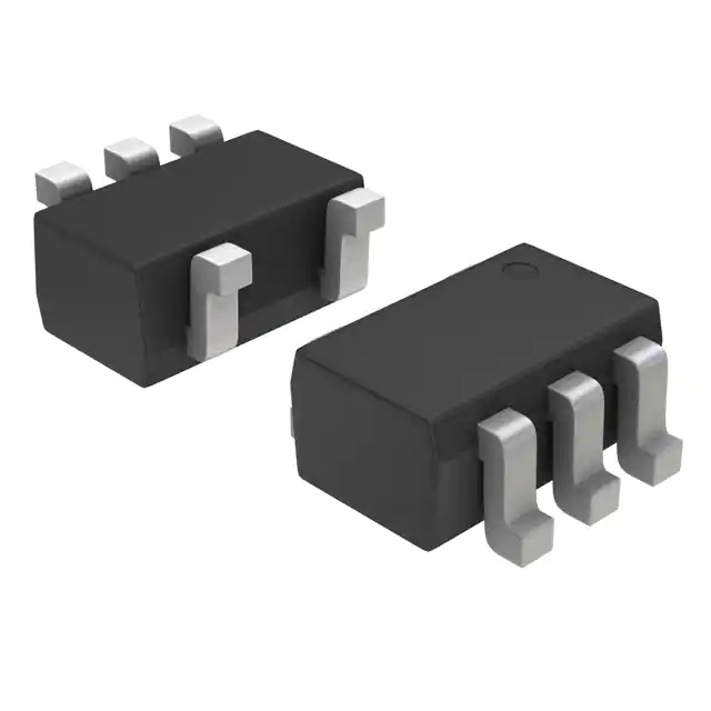
- Part No.:
- NCP502SQ36T1G
- Manufacturer:
- onsemi
- Package:
- 5-TSSOP, SC-70-5, SOT-353
- Datasheet:
-
 NCP502SQ36T1G.pdf
- Description:
- IC REG LINEAR 3.6V 80MA SC88A
- Quantity:
- Payment:

- Shipping:

Inventory:1,249
Please send an inquiry. Send us your inquiry, and we will respond immediately.
Product details
Overview
NCP502SQ36T1G from onsemi is a fixed-output, low-quiescent-current CMOS linear voltage regulator delivering 3.6 V at up to 80 mA with ultra-low 40 µA typical quiescent current, housed in SC70-5 package. It features PMOS pass transistor architecture, ±2.0% output voltage accuracy over temperature, and operates across −40 °C to +85 °C for battery-powered portable instrumentation.
For engineers reviewing the NCP502SQ36T1G datasheet, pinout, applications, or equivalent options, key selection criteria include dropout voltage at 80 mA (max 850 mV), enable threshold compatibility (1.3 V high / 0.3 V low), thermal shutdown protection, and ceramic capacitor stability without ESR constraints.
Technical Context
The NCP502SQ36T1G implements a PMOS-based LDO topology with internal voltage reference, error amplifier, and protection circuitry including current limit and thermal shutdown. Its enable input provides logic-controlled standby mode with defined turn-on/turn-off thresholds.
Designed for low-noise, low-power operation, it achieves 55 dB ripple rejection at 1 kHz and 180 µVRMS output noise (100 Hz–100 kHz), while maintaining regulation with input voltages up to 12 V and supporting ceramic output capacitors ≥1.0 µF without stability constraints.
Key Specifications
| Parameter | Value and Actual Design Meaning |
|---|---|
| Output Voltage | Fixed 3.6 V ±2.0% over −40 °C to +85 °C - ensures stable rail for 3.3 V–3.6 V logic and analog subsystems. |
| Max Output Current | 80 mA - sufficient for microcontrollers, sensors, and RF front-end biasing in compact portable devices. |
| Quiescent Current | 40 µA typical - enables multi-year battery life in always-on monitoring applications with intermittent wake-up. |
| Dropout Voltage | 850 mV max at 80 mA - allows operation from single-cell Li-ion (3.0 V min) or two-cell alkaline (3.2 V min) sources. |
| Ripple Rejection | 55 dB at 1 kHz - suppresses switching noise from upstream DC-DC converters feeding the LDO input. |
| Thermal Shutdown | Activates at ~160 °C - protects against sustained overload or poor PCB thermal design without external circuitry. |
| Enable Threshold | 1.3 V (high), 0.3 V (low) - compatible with 1.8 V and 3.3 V GPIOs for precise power sequencing control. |
Pinout & Package
Package: SC70-5 (Case 419A), 1.25 mm × 1.65 mm × 0.95 mm, Pb-free, surface-mount.
| Pin/Terminal | Circuit Role | Design Meaning |
|---|---|---|
| 1 | Vin | Positive input supply - accepts 3.6 V to 12 V; must be decoupled with ≥1.0 µF ceramic capacitor near pin. |
| 2 | GND | Power ground reference - requires low-impedance connection to minimize noise coupling and ensure regulation accuracy. |
| 3 | Enable | Active-high digital control - pulls device into low-power standby when <0.3 V; connect to Vin if unused. |
| 4 | N/C | No internal connection - no PCB trace or pad required; floating or grounded per layout convenience. |
| 5 | Vout | Regulated 3.6 V output - drives load directly; supports ≥1.0 µF ceramic output capacitor for transient response and noise filtering. |
Key Features
| Feature | Design Value |
|---|---|
| Ultra-low quiescent current | 40 µA typical - extends battery runtime in IoT edge nodes and wearable health monitors. |
| Ceramic capacitor compatibility | Stable with 1.0 µF ceramic output cap (no ESR minimum) - reduces BOM cost and board area vs. tantalum alternatives. |
| High output accuracy | ±2.0% over full temperature range - eliminates need for post-regulation trimming in precision analog signal chains. |
| Integrated protection | Current limit + thermal shutdown - prevents damage during short-circuit or thermal overload without external components. |
| Low-noise regulation | 180 µVRMS output noise (100 Hz–100 kHz) - suitable for powering ADC references and RF synthesizer VCOs. |
Applications
| Portable Medical Sensors | Wireless Remote Controls |
|---|---|
|
Use Scenario: Continuous glucose monitor (CGM) sensor node powered by coin cell, sampling every 5 minutes. IC Role / Device Role / Timing Role: Primary 3.6 V supply for ultra-low-power MCU and analog front-end amplifier. Use Value: 40 µA quiescent current enables >3-year battery life; ±2.0% output accuracy maintains ADC linearity across body temperature range. |
Use Scenario: Sub-GHz RF remote with push-button wake-up and BLE advertisement burst. IC Role / Device Role / Timing Role: Standby power regulator enabling fast wake-up from deep-sleep state via Enable pin control. Use Value: 1.3 V enable threshold matches 1.8 V MCU GPIO; 850 mV dropout permits operation down to 2.75 V battery voltage. |
| Handheld Test Meters | Smart Home Motion Sensors |
|
Use Scenario: Battery-operated multimeter with LCD display and auto-ranging analog circuitry. IC Role / Device Role / Timing Role: Clean 3.6 V rail for precision op-amps and 16-bit SAR ADC reference buffer. Use Value: 180 µVRMS noise and 55 dB ripple rejection prevent switching artifacts from corrupting measurement resolution. |
Use Scenario: PIR-based occupancy detector with motion-triggered LED indicator and Zigbee reporting. IC Role / Device Role / Timing Role: Always-on regulator supplying real-time clock and low-power sensor interface. Use Value: SC70-5 footprint minimizes PCB area in space-constrained housing; thermal shutdown prevents latch-up during enclosure overheating. |
Equivalent & Alternatives
The following parts are listed as comparable options for similar LDO regulator applications.
| Alternative Part | Technical Difference | Application Difference | Selection Advice |
|---|---|---|---|
| MCP1700T-3602E/TT | 300 mA output, 1.6 µA quiescent current, SOT-23-3 package (no enable) | Lacks enable pin and thermal shutdown; higher output current but larger package | Select when ultra-low IQ dominates and enable control is unnecessary; verify thermal margin at 80 mA. |
| TN0360S | 3.6 V fixed, 100 mA, 50 µA IQ, TSOP-5 package, AEC-Q100 qualified | Automotive-grade variant with extended temp range (−40 °C to +125 °C) and PPAP support | Prefer for automotive cabin modules where qualification and higher ambient tolerance are mandatory. |
Compared with MCP1700T-3602E/TT and TN0360S, the NCP502SQ36T1G offers optimal balance of enable functionality, thermal safety, SC70-5 miniaturization, and industrial temperature compliance - making it ideal for space- and battery-life-constrained consumer portables.
Availability
NCP502SQ36T1G is available at Aetrix Electronics and suitable for portable medical sensors, wireless remote controls, handheld test meters, smart home motion sensors, and other battery-powered embedded systems requiring stable component supply with long lifecycle visibility.
Supply support for NCP502SQ36T1G includes scheduled delivery planning, volume procurement assistance, BOM continuity management, traceable sourcing, and lifecycle availability coordination for OEM customers, industrial embedded developers, connected-device designers, and electronics production programs.
Manufacturer
onsemi (formerly ON Semiconductor) is a global semiconductor supplier specializing in energy-efficient power management, analog, sensing, and connectivity solutions for automotive, industrial, and consumer markets.
The NCP502 series belongs to onsemi's low-power linear regulator product line, engineered specifically for handheld communication equipment and portable battery-powered devices demanding ultra-low quiescent current and small-footprint packaging.
FAQ
What is the maximum input voltage rating for the NCP502SQ36T1G?
The NCP502SQ36T1G has an absolute maximum input voltage of 12 V, as specified in the Maximum Ratings table. Operation above this level risks permanent damage. For reliable long-term use, design with headroom - e.g., 3.6 V output + 850 mV dropout implies minimum Vin = 4.45 V, so 5–9 V supplies are typical in practice.
Does the NCP502SQ36T1G require an external output capacitor, and what value is recommended?
Yes, the NCP502SQ36T1G requires an external output capacitor for stability and transient performance. The datasheet specifies a minimum of 1.0 µF ceramic capacitor, placed close to the Vout and GND pins. Larger values improve load transient response and noise filtering; no ESR minimum is required, enabling low-cost X5R/X7R MLCCs.
Can the NCP502SQ36T1G be used without connecting the Enable pin?
Yes - if the Enable function is not needed, the Enable pin (Pin 3) must be connected directly to Vin to ensure the device remains active. Leaving it floating is not permitted, as undefined logic levels may cause erratic enable/disable behavior or increased leakage current.
What is the thermal resistance (RJA) of the NCP502SQ36T1G in its SC70-5 package?
The NCP502SQ36T1G in SC70-5 (Case 419A) has a junction-to-ambient thermal resistance (RJA) of 400 °C/W under standard test conditions (single component on 80 × 80 mm FR4 PCB with 1 oz copper). This value assumes minimal copper pour; adding thermal vias and copper planes significantly improves heat dissipation.
Is the NCP502SQ36T1G RoHS-compliant and lead-free?
Yes, the NCP502SQ36T1G is a Pb-free device compliant with RoHS Directive 2011/65/EU. The "G" suffix in the part number explicitly denotes lead-free packaging, and the datasheet confirms it meets JEDEC J-STD-020 moisture sensitivity level 1 (MSL1) requirements.
NCP502SQ36T1G Specifications
- Product attributes
- Attribute value
- Manufacturer:
- onsemi
- Series:
- -
- Package/Case:
- 5-TSSOP, SC-70-5, SOT-353
- Packaging:
- Tape & Reel (TR)
- Product Status:
- Obsolete
- Output Configuration:
- Positive
- Output Type:
- Fixed
- Number of Regulators:
- 1
- Voltage - Input (Max):
- 12V
- Voltage - Output (Min/Fixed):
- 3.6V
- Voltage - Output (Max):
- -
- Voltage Dropout (Max):
- 1.2V @ 80mA
- Current - Output:
- 80mA
- Current - Quiescent (Iq):
- 40 µA
- Current - Supply (Max):
- 90 µA
- PSRR:
- 55dB (1kHz)
- Control Features:
- Enable
- Protection Features:
- Over Current, Over Temperature
- Operating Temperature:
- -40°C ~ 85°C
- Grade:
- -
- Qualification:
- -
- Mounting Type:
- Surface Mount
- Supplier Device Package:
- SC-88A (SC-70-5/SOT-353)
NCP502SQ36T1G FAQ
1.How can I place an order for NCP502SQ36T1G through Aetrix?
Please submit a Request for Quotation (RFQ) for NCP502SQ36T1G on Aetrix. Our sales agent will provide a competitive quotation and guide you through the order confirmation once you accept the terms.
2.Are the price and stock information for NCP502SQ36T1G reliable?
The price and inventory of NCP502SQ36T1G are updated periodically and may fluctuate due to market conditions. Stock and pricing data are typically refreshed every 24 hours. Quotation validity for NCP502SQ36T1G is usually 5 days.
3.What payment methods are accepted for NCP502SQ36T1G?
We accept Wire Transfer, PayPal, Credit Card, Western Union, MoneyGram, and Escrow for NCP502SQ36T1G transactions.
Note: Certain payment methods may incur a processing fee.
4.How is shipping managed for NCP502SQ36T1G?
NCP502SQ36T1G orders can be shipped via leading logistics carriers, including DHL, UPS, FedEx, TNT, or Registered Mail.
Once your NCP502SQ36T1G order is processed, you will receive an email with the shipment details and tracking number.
Note: Tracking information may take up to 24 hours to appear. Express delivery typically takes 3–5 business days.
5.How can I obtain technical support or documentation for NCP502SQ36T1G?
For technical support, including NCP502SQ36T1G datasheets, pinout diagrams, or application guidance, please contact our engineering support team. They can provide detailed documentation and assistance for your NCP502SQ36T1G requirements.
6.How does Aetrix verify that NCP502SQ36T1G is sourced from the original manufacturer or authorized distributors?
All NCP502SQ36T1G products on Aetrix are procured from qualified distributors and authorized channels. Our dedicated quality assurance team conducts strict verification, including traceability checks and, if necessary, third-party testing. This ensures that NCP502SQ36T1G meets industry standards.
7.What is the process for return or replacement of NCP502SQ36T1G?
All NCP502SQ36T1G units undergo pre-shipment inspection (PSI). If there is an issue with NCP502SQ36T1G, returns or replacements are accepted under the following conditions:
1.Quantity discrepancies, incorrect items, or visible external defects (such as breakage or corrosion), acknowledged by Aetrix.
2.The issue is reported within 90 days of delivery.
3.The NCP502SQ36T1G part is unused and in its original packaging.
Return procedure for NCP502SQ36T1G:
1.Submit a request within 90 days.
2.Obtain a Return Material Authorization (RMA) from Aetrix.
NCP502SQ36T1G Tags

-
MIC5504-1.8YM5-TR
Microchip Technology
-
MIC5504-3.3YM5-TR
Microchip Technology

-
MIC5365-3.0YC5-TR
Microchip Technology
-
MIC5365-1.8YC5-TR
Microchip Technology
-
MIC5365-2.5YC5-TR
Microchip Technology
-
MIC5365-3.3YC5-TR
Microchip Technology

-
MIC5365-3.3YD5-TR
Microchip Technology

-
MIC5317-3.3YM5-TR
Microchip Technology

-
TLV1117LV33DCYR
Texas Instruments

-
MIC5317-3.3YMT-TZ
Microchip Technology

-
MIC5528-3.3YMT-TR
Microchip Technology

-
TLV75801PDRVR
Texas Instruments
Tech Hub

Counterfeit components can hide behind convincing markings and passing basic function tests. This engineering reference covers source traceability, external inspection, X-ray, XRF, electrical testing, …

A practical engineering and sourcing framework covering lifecycle verification, lifetime-buy calculations, replacement qualification, supplier checks and counterfeit-risk controls.

TTL and CMOS logic families differ in thresholds, loading, output drive, power and timing. This engineering guide compares 74HC and 74HCT, calculates noise margins and checks 3.3 V/5 V compatibility.

A practical engineering guide to 3.3V and 5V logic compatibility, input thresholds, resistor dividers, translator ICs, MOSFET level shifting, I2C pull-ups, timing limits and power-sequencing risks.

The 74HC595 uses push-pull logic outputs, while the TPIC6B595 uses 50 V open-drain DMOS sinks for higher-power loads. This guide compares timing, current limits, 3.3 V interfacing, load wiring, thermal…

The 74HC595 converts serial data into eight stable parallel outputs. This guide covers pin functions, shift and storage timing, OE and MR behavior, drive-current limits, cascading, voltage compatibilit…

A technical comparison of level-sensitive latches and edge-triggered flip-flops, covering timing windows, setup and hold limits, master–slave operation, time borrowing, race-through, HDL inference and…

A D latch stores one bit while Enable controls when data can pass. This reference covers gate-level operation, truth tables, transparency, setup and hold timing, LE versus OE, common ICs and practical …

An SR latch stores one bit through cross-coupled feedback. This engineering reference covers NOR and NAND implementations, truth tables, forbidden-state recovery, gated operation, switch debouncing, fa…

Latch circuits retain one bit through feedback. This technical reference covers SR and D latches, truth tables, transparency, timing limits, latch-versus-flip-flop behavior, applications and common log…


