
 My Inquiry
 My Account


onsemi NCP5314FTR2
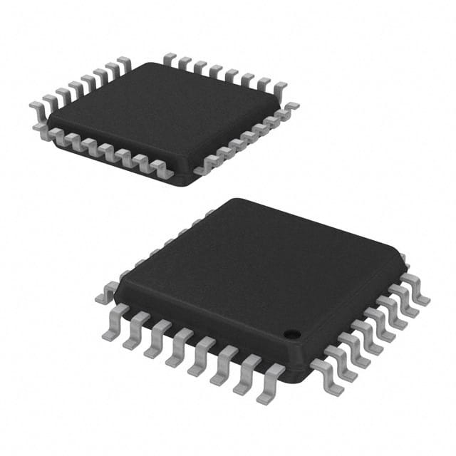
- Part No.:
- NCP5314FTR2
- Manufacturer:
- onsemi
- Category:
- Special Purpose Regulators
- Package:
- 32-LQFP
- Datasheet:
-
 NCP5314FTR2.pdf
- Description:
- IC REG CTRLR CPU 4OUT 32LQFP
- Quantity:
- Payment:

- Shipping:

Inventory:1,330
Please send an inquiry. Send us your inquiry, and we will respond immediately.
Product details
Overview
NCP5314FTR2 from onsemi is a programmable two/three/four-phase buck CPU controller for high-performance x86 processors, supporting VR(M)10.x compliance with 6-bit VID DAC (0.8375–1.6000 V output range), up to 1.2 MHz per-phase switching frequency, and enhanced V2™ control for sub-100 ns transient response. It integrates differential current sensing per phase, adaptive voltage positioning, and latching overvoltage/overcurrent protection - deployed in server CPU VRMs and high-end desktop power delivery.
For engineers reviewing the NCP5314FTR2 datasheet, pinout, applications, or equivalent options, this page delivers verified technical context, phase-configurable operation details, real-world current-sharing performance (≤10% inter-phase mismatch), and VR(M)10.x-compliant power sequencing behavior - critical for CPU core voltage regulation design validation.
Technical Context
The NCP5314FTR2 implements Enhanced V2™ control combining fast voltage feedback (via VFFB direct connection to PWM comparator) with peak current-mode sensing across four phases. Its internal ramp (100 mV at 50% duty) compensates propagation delays, enabling stable operation down to 40 ns minimum pulse width and duty cycles above 50% without external slope compensation.
Phase timing is fixed-frequency with 90° inter-phase delay in 4-phase mode (120° in 3-phase), driven by ROSC-set oscillator (660 kHz typical at 32.4 kΩ). Current sharing is enforced by referencing all phase comparators to a common COMP node and using differential CSxP/CSxN inputs with 2.54 V/V gain to VDRP for adaptive voltage positioning.
Key Specifications
| Parameter | Value and Actual Design Meaning |
|---|---|
| Output Voltage Range | 0.8375 V to 1.6000 V via 6-bit VID DAC; supports VR(M)10.x CPU voltage scaling with ±0.5% code accuracy. |
| Phase Configuration | Programmable 2-, 3-, or 4-phase operation; enables scalable current handling and ripple reduction in CPU VRMs. |
| Switching Frequency | Up to 1.2 MHz per phase; ROSC resistor sets frequency (660 kHz typical in 4-phase, 880 kHz in 3-phase). |
| Current Sharing Accuracy | ≤10% mismatch between phases; achieved via differential current sense amplifiers and shared COMP node. |
| Transient Response Time | ≤60 ns from current step to gate response; enabled by fast voltage feedback path through VFFB pin. |
| Protection Features | Latching OVP (200 mV above VID), programmable pulse-by-pulse current limit (90 mV threshold), UVLO (9.0 V start), and "111110"/"111111" DAC fault detection. |
| Package | LQFP-32 (Case 873A); Pb-free option available as NCP5314FTR2G. |
Pinout & Package
LQFP-32 package (Case 873A), 10 mm × 10 mm body, 0.8 mm pitch, exposed thermal pad (not electrically connected). Pin 1 marked by dot; pin numbering follows standard LQFP counterclockwise from top-left corner.
| Pin/Terminal | Circuit Role | Design Meaning |
|---|---|---|
| VID0–VID5 | DAC voltage identification inputs | Logic-level inputs defining output voltage per VR(M)10.x; all high on VID0–VID4 triggers fault. |
| VFB | Error amplifier inverting input | Primary feedback node for slow-loop regulation; referenced to SGND for remote sensing. |
| VFFB | Fast voltage feedback input | Direct connection to PWM comparator non-inverting input for <60 ns load-step response. |
| GATE1–GATE4 | PWM channel outputs | High-speed gate drive signals (2.7 V high, 0.7 V low) for external MOSFET drivers; 5 ns rise/fall time. |
| CS1P–CS4P / CS1N–CS4N | Differential current sense inputs | Per-phase inductor current measurement; enables lossless sensing and ≤10% inter-phase current match. |
| COMP | Error amplifier output & PWM comparator input | Loop compensation node; clamped during soft-start/fault; shared across all phases for current balancing. |
| DRVON | MOSFET driver enable | Active-high logic signal (2.3 V min high) that forces all GATEx outputs low when deasserted. |
| PWRGD | Open-collector power-good output | Indicates regulation status (50–600 μs delay); asserts high when VOUT within ±115 mV of VID setpoint. |
Key Features
| Feature | Design Value |
|---|---|
| Enhanced V2™ Control | Combines fast voltage feedback (VFFB) and peak current-mode sensing for <60 ns transient response and inherent line/load regulation. |
| Adaptive Voltage Positioning (AVP) | VDRP output provides dynamic offset proportional to total inductor current, reducing output capacitor count by up to 30% in high-dI/dt CPU loads. |
| Programmable Soft-Start | SS pin controls linear voltage ramp via external capacitor; charge current = 44 μA typical, enabling precise inrush current limiting. |
| VR(M)10.x Compliance | 6-bit VID DAC with 0.5% tolerance, power-good thresholds aligned to VR10 spec, and "111110"/"111111" DAC fault codes for processor handshake. |
| Differential Current Sensing | Four independent CSxP/CSxN pairs with 3.1× gain and 7 MHz bandwidth deliver accurate per-phase current data for tight sharing (<10%). |
Applications
| Server CPU VRM | High-End Desktop Motherboard |
|---|---|
|
Use Scenario: Regulating core voltage for dual-socket Xeon Scalable processors under dynamic 200 A+ load steps. IC Role / Device Role / Timing Role: Primary multi-phase buck controller managing four parallel power stages with synchronized 90° phase shift. Use Value: Achieves <60 ns transient response and ≤10% inter-phase current imbalance, reducing required bulk capacitance by 35% versus single-phase designs. |
Use Scenario: Delivering tightly regulated 1.2–1.4 V to AMD Ryzen or Intel Core i9 CPUs during gaming workloads with rapid P-state transitions. IC Role / Device Role / Timing Role: VR(M)10.x-compliant CPU voltage controller with adaptive voltage positioning and programmable soft-start sequencing. Use Value: Enables precise AVP implementation via VDRP pin, lowering output ripple by 25% and eliminating need for external current-sense resistors. |
| Workstation GPU Power | AI Accelerator Board |
|
Use Scenario: Supplying 0.8–1.1 V to high-TDP GPUs (e.g., NVIDIA A100) requiring >500 W with strict voltage tolerance (±15 mV). IC Role / Device Role / Timing Role: Four-phase buck controller with latching OVP (200 mV above VID) and pulse-by-pulse current limiting per phase. Use Value: Provides hardware-level fault protection that shuts down within 500 μs of overvoltage, preventing GPU rail damage during transient events. |
Use Scenario: Powering FPGA-based AI inference accelerators with bursty 100+ A current demands and strict sequencing requirements. IC Role / Device Role / Timing Role: Multi-phase controller with ENABLE-driven power-up sequencing and PWRLS-sensed lower power-good threshold. Use Value: Supports system-level sequencing via ENABLE pin tied to FPGA DONE signal, ensuring stable VCORE before logic initialization. |
Equivalent & Alternatives
The following parts are listed as comparable options for similar multi-phase CPU buck controller applications.
| Alternative Part | Technical Difference | Application Difference | Selection Advice |
|---|---|---|---|
| ISL6322IRZ | 3-phase only; uses traditional V2 control (no internal ramp); 8-bit VID (0.3–2.0 V); no AVP support. | Lacks adaptive voltage positioning and 4-phase capability; requires external slope compensation above 500 kHz. | Select when 3-phase operation suffices and AVP is not required; verify compatibility with existing layout due to different pinout and feedback architecture. |
| RT8803AZSP | 4-phase with D-CAP+ control; 6-bit VID; integrated MOSFET drivers; no differential current sense pins. | Eliminates need for external gate drivers but lacks per-phase current monitoring and fine-grained current sharing tuning. | Choose for space-constrained designs where integrated drivers reduce BOM count; avoid if precise inter-phase current matching or external driver flexibility is required. |
Compared with ISL6322IRZ and RT8803AZSP, the NCP5314FTR2 uniquely combines 4-phase configurability, differential current sensing for ≤10% sharing accuracy, and Enhanced V2™ with internal ramp - enabling higher-frequency operation without slope compensation while maintaining VR(M)10.x compliance and AVP capability.
Availability
NCP5314FTR2 is available at Aetrix Electronics and suitable for server CPU VRMs, high-end desktop motherboards, and AI accelerator boards requiring stable component supply, long-term lifecycle support, and traceable sourcing for industrial and enterprise deployments.
Supply support for NCP5314FTR2 includes scheduled delivery planning, volume procurement assistance, BOM continuity management, traceable sourcing, and lifecycle availability coordination for OEM customers, industrial embedded developers, connected-device designers, and electronics production programs.
Manufacturer
onsemi (formerly ON Semiconductor) is a global semiconductor supplier specializing in energy-efficient power management, analog, sensor, and connectivity solutions for automotive, industrial, cloud, and consumer markets.
The NCP5314FTR2 belongs to onsemi's high-performance CPU voltage regulator controller product line, designed specifically for VR(M)10.x-compliant multi-phase buck converters in servers, workstations, and high-end computing platforms.
FAQ
What is the maximum supported switching frequency per phase for the NCP5314FTR2?
The NCP5314FTR2 supports up to 1.2 MHz per phase in two-phase configuration. In three-phase mode, typical frequency is 880 kHz; in four-phase mode, it is 660 kHz - both set by the ROSC resistor value (e.g., 32.4 kΩ yields 660 kHz in 4-phase). The oscillator tolerances are ±15%, and frequency decreases with added phase count due to internal timing division.
How does the NCP5314FTR2 achieve current sharing between phases?
The NCP5314FTR2 achieves current sharing via differential current sense inputs (CS1P/CS1N through CS4P/CS4N) feeding individual current sense amplifiers, whose outputs sum into the shared COMP node. This forces all phases to regulate to the same COMP voltage, causing higher-current phases to terminate earlier - achieving ≤10% inter-phase current mismatch without external balancer circuits.
Does the NCP5314FTR2 support VR(M)10.x specifications?
Yes, the NCP5314FTR2 fully supports VR(M)10.x specifications: it includes a 6-bit VID DAC compatible with VR10 protocols, power-good thresholds aligned to VR10 (±115 mV upper, 50% lower), "111110" and "111111" DAC fault codes, adaptive voltage positioning, and required protection features including latching OVP and programmable overcurrent limits.
What is the function of the VDRP pin on the NCP5314FTR2?
The VDRP pin on the NCP5314FTR2 outputs an analog voltage proportional to total inductor current (summed across all phases), used for adaptive voltage positioning (AVP). Its offset above the DAC voltage is programmable via an external resistor to VFB; when enabled, it lowers VCORE under load to maintain constant effective output impedance - reducing required output capacitance by up to 30%.
Can the NCP5314FTR2 operate in two-phase mode, and how is it configured?
Yes, the NCP5314FTR2 supports two-phase operation. It is configured by leaving CS3P/CS3N and CS4P/CS4N unconnected (high-impedance), which disables Phases 3 and 4. The remaining CS1P/CS1N and CS2P/CS2N pairs remain active, and the internal oscillator automatically adjusts timing for 180° phase separation. No register programming or external strapping is required - mode is determined by connected current sense inputs.
NCP5314FTR2 Specifications
- Product attributes
- Attribute value
- Manufacturer:
- onsemi
- Series:
- -
- Package/Case:
- 32-LQFP
- Packaging:
- Tape & Reel (TR)
- Product Status:
- Obsolete
- Applications:
- Controller, CPU
- Voltage - Input:
- 9.5V ~ 13.2V
- Number of Outputs:
- 4
- Voltage - Output:
- -
- Operating Temperature:
- 0°C ~ 70°C
- Grade:
- -
- Qualification:
- -
- Mounting Type:
- Surface Mount
- Supplier Device Package:
- 32-LQFP (7x7)
NCP5314FTR2 FAQ
1.How can I place an order for NCP5314FTR2 through Aetrix?
Please submit a Request for Quotation (RFQ) for NCP5314FTR2 on Aetrix. Our sales agent will provide a competitive quotation and guide you through the order confirmation once you accept the terms.
2.Are the price and stock information for NCP5314FTR2 reliable?
The price and inventory of NCP5314FTR2 are updated periodically and may fluctuate due to market conditions. Stock and pricing data are typically refreshed every 24 hours. Quotation validity for NCP5314FTR2 is usually 5 days.
3.What payment methods are accepted for NCP5314FTR2?
We accept Wire Transfer, PayPal, Credit Card, Western Union, MoneyGram, and Escrow for NCP5314FTR2 transactions.
Note: Certain payment methods may incur a processing fee.
4.How is shipping managed for NCP5314FTR2?
NCP5314FTR2 orders can be shipped via leading logistics carriers, including DHL, UPS, FedEx, TNT, or Registered Mail.
Once your NCP5314FTR2 order is processed, you will receive an email with the shipment details and tracking number.
Note: Tracking information may take up to 24 hours to appear. Express delivery typically takes 3–5 business days.
5.How can I obtain technical support or documentation for NCP5314FTR2?
For technical support, including NCP5314FTR2 datasheets, pinout diagrams, or application guidance, please contact our engineering support team. They can provide detailed documentation and assistance for your NCP5314FTR2 requirements.
6.How does Aetrix verify that NCP5314FTR2 is sourced from the original manufacturer or authorized distributors?
All NCP5314FTR2 products on Aetrix are procured from qualified distributors and authorized channels. Our dedicated quality assurance team conducts strict verification, including traceability checks and, if necessary, third-party testing. This ensures that NCP5314FTR2 meets industry standards.
7.What is the process for return or replacement of NCP5314FTR2?
All NCP5314FTR2 units undergo pre-shipment inspection (PSI). If there is an issue with NCP5314FTR2, returns or replacements are accepted under the following conditions:
1.Quantity discrepancies, incorrect items, or visible external defects (such as breakage or corrosion), acknowledged by Aetrix.
2.The issue is reported within 90 days of delivery.
3.The NCP5314FTR2 part is unused and in its original packaging.
Return procedure for NCP5314FTR2:
1.Submit a request within 90 days.
2.Obtain a Return Material Authorization (RMA) from Aetrix.
NCP5314FTR2 Tags

-
TPS51206DSQR
Texas Instruments

-
TPS51200DRCR
Texas Instruments
-
TPS51200DRCT
Texas Instruments

-
TPS62740DSSR
Texas Instruments

-
TPS51100DGQR
Texas Instruments

-
NCP51200MNTXG
onsemi
-
NCP51400MNTXG
onsemi

-
RT9026GSP
Richtek USA Inc.

-
LP2998MRX/NOPB
Texas Instruments
-
TPS51200QDRCRQ1
Texas Instruments

-
DPA423GN-TL
Power Integrations
-
LM10011SD/NOPB
Texas Instruments
Tech Hub

Counterfeit components can hide behind convincing markings and passing basic function tests. This engineering reference covers source traceability, external inspection, X-ray, XRF, electrical testing, …

A practical engineering and sourcing framework covering lifecycle verification, lifetime-buy calculations, replacement qualification, supplier checks and counterfeit-risk controls.

TTL and CMOS logic families differ in thresholds, loading, output drive, power and timing. This engineering guide compares 74HC and 74HCT, calculates noise margins and checks 3.3 V/5 V compatibility.

A practical engineering guide to 3.3V and 5V logic compatibility, input thresholds, resistor dividers, translator ICs, MOSFET level shifting, I2C pull-ups, timing limits and power-sequencing risks.

The 74HC595 uses push-pull logic outputs, while the TPIC6B595 uses 50 V open-drain DMOS sinks for higher-power loads. This guide compares timing, current limits, 3.3 V interfacing, load wiring, thermal…

The 74HC595 converts serial data into eight stable parallel outputs. This guide covers pin functions, shift and storage timing, OE and MR behavior, drive-current limits, cascading, voltage compatibilit…

A technical comparison of level-sensitive latches and edge-triggered flip-flops, covering timing windows, setup and hold limits, master–slave operation, time borrowing, race-through, HDL inference and…

A D latch stores one bit while Enable controls when data can pass. This reference covers gate-level operation, truth tables, transparency, setup and hold timing, LE versus OE, common ICs and practical …

An SR latch stores one bit through cross-coupled feedback. This engineering reference covers NOR and NAND implementations, truth tables, forbidden-state recovery, gated operation, switch debouncing, fa…

Latch circuits retain one bit through feedback. This technical reference covers SR and D latches, truth tables, transparency, timing limits, latch-versus-flip-flop behavior, applications and common log…


