
 My Inquiry
 My Account


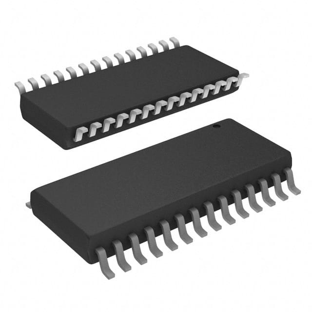
onsemi NCP5322ADWR2
- Part No.:
- NCP5322ADWR2
- Manufacturer:
- onsemi
- Category:
- Special Purpose Regulators
- Package:
- 28-SOIC (0.295", 7.50mm Width)
- Datasheet:
-
 NCP5322ADWR2.pdf
- Description:
- IC REG CTRLR HI PERF 2OUT 28SOIC
- Quantity:
- Payment:

- Shipping:

Inventory:1,542
Please send an inquiry. Send us your inquiry, and we will respond immediately.
Product details
Overview
NCP5322ADWR2 from ON Semiconductor is a second-generation, two-phase synchronous buck controller with integrated high- and low-side gate drivers, 5-bit VID DAC (±1.0% accuracy), and Enhanced V² control architecture. It delivers tightly regulated output voltages from 1.089 V to 1.869 V for high-performance processors and core logic in server, desktop, and embedded computing systems requiring up to 45 A total output current.
For engineers reviewing the NCP5322ADWR2 datasheet, pinout, applications, or equivalent options, key selection considerations include its 200–800 kHz adjustable switching frequency, adaptive voltage positioning (AVP) support via VDRP, dual-phase current balancing, hiccup-mode overcurrent protection, and SO-28L package compatibility with high-density PCB layouts.
Technical Context
The NCP5322ADWR2 implements an Enhanced V² control architecture combining fast-feedback directly from VCORE with an internal PWM ramp and traditional error amplifier regulation. This enables sub-cycle transient response and eliminates need for external slope compensation.
Its two-phase operation uses 180° phase delay between GATE(H)1/GATE(L)1 and GATE(H)2/GATE(L)2, with shared CSREF and COMP nodes enabling precise current sharing. Each phase features independent ILIM threshold setting, on-board current sense amplifiers (3.5 V/V gain), and individual hiccup-mode current limiting.
Key Specifications
| Parameter | Value and Actual Design Meaning |
|---|---|
| Topology | Two-phase synchronous buck controller with integrated gate drivers for high-side and low-side MOSFETs per phase. |
| Output Voltage Range | 1.089 V to 1.869 V (25-step 5-bit VID DAC, ±1.0% accuracy at all codes). |
| Switching Frequency | 200–800 kHz (set by ROSC resistor; typical 400 kHz at ROSC = 32.4 kΩ). |
| Current Sensing | Differential current sense inputs (CS1/CS2) with on-chip amplifiers (3.5 V/V gain); supports resistive or inductive sensing. |
| Adaptive Voltage Positioning | VDRP pin provides current-proportional offset (2.6–4.0 V/V gain) for dynamic VOUT droop under load. |
| Protection Features | Hiccup-mode overcurrent (per-phase pulse-by-pulse limit at 90–135 mV CSx–CSREF), PWRGD with 60–240 µs fault delay, UVLO on VCCL (4.05–4.5 V start) and VCCH1 (1.8–2.2 V start). |
| Package | SO-28L (Case 751F), Pb-free, 1000-piece tape-and-reel (NCP5322ADWR2). |
Pinout & Package
SO-28L package (Case 751F), 300 mil body width, 1.27 mm pitch, exposed thermal pad not present. Pin 1 marked with dot; pin 1 is COMP.
| Pin/Terminal | Circuit Role | Design Meaning |
|---|---|---|
| COMP | Error amplifier output / PWM comparator input | Drives external compensation network; clamped during soft-start and hiccup mode. |
| VFB | Voltage feedback node | Connects to output divider; shorted to VOUT for no AVP, or to VDRP resistor for adaptive droop. |
| VDRP | AVP current-sense output | Provides current-proportional offset (max 2.3 V); used to set VOUT droop slope via resistor to VFB. |
| CS1, CS2 | Per-phase current sense inputs | Differential inputs referenced to CSREF; must stay within ±105 mV of CSREF to avoid false current-limit trips. |
| CSREF | Current sense reference / PWRGD comparator input | Reference for both current sense amps and PWRGD; sets fast-feedback path to PWM comparator. |
| PWRGD | Open-drain power-good output | Asserts low when VOUT deviates >±12% from DAC-set voltage; 60–240 µs delay ensures stable startup. |
| VID0–VID4 | 5-bit voltage ID inputs | Set DAC output (1.089–1.869 V); internally pulled up to 3.3 V; compatible with Intel VRM 10.x protocols. |
| ILIM | Per-phase current limit threshold | Resistive divider from REF sets trip point (0.25–1.0 V range); gain 5.5–8.5 V/V into internal comparator. |
| REF | 3.3 V reference output | Stable 3.3 V ±3%, 1 mA max sink/source; decoupled with 0.1 µF to LGND. |
| GATE(H)1/2, GATE(L)1/2 | Integrated MOSFET gate drivers | Each driver delivers 200 mA DC / 1.5 A peak; rise/fall times ≤80 ns (1–8 V swing, 10 V supply). |
| VCCH1/2, VCCL1/2 | Driver supply rails | VCCHx powers high-side drivers (UVLO: 1.8–2.2 V); VCCLx powers low-side drivers (UVLO: 4.05–4.5 V). |
| SS | Soft-start timing capacitor | Controls startup ramp time and hiccup frequency; clamps COMP below SS voltage during startup/fault. |
| ROSC | Oscillator frequency set | Resistor to ground sets fSW (200–800 kHz) and scales VFB bias current (10–80 µA range). |
Key Features
| Feature | Design Value |
|---|---|
| Enhanced V² Control with Internal Ramp | Enables <1-cycle transient response and eliminates need for external slope compensation; supports >50% duty cycles at high fSW. |
| 5-Bit VID DAC with ±1.0% Accuracy | Directly programs 25 discrete output voltages (1.089–1.869 V) meeting Intel VRM 10.x specifications for CPU core supplies. |
| Adaptive Voltage Positioning (AVP) | VDRP pin provides current-proportional offset (2.6–4.0 V/V gain) to implement controlled VOUT droop under load, reducing output capacitance requirements. |
| Dual-Phase Current Sharing | Shared CSREF and COMP ensure balanced load distribution across phases; mismatch <±5 mV (gain + offset) guarantees <3% current imbalance. |
| Integrated Gate Drivers | Four drivers (2× high-side, 2× low-side) with 200 mA DC drive capability reduce external component count and improve layout integrity. |
| Hiccup-Mode Overcurrent Protection | Per-phase pulse-by-pulse current limiting (trip at 90–135 mV CSx–CSREF) plus hiccup recovery prevents thermal runaway during sustained overload. |
Applications
| Server CPU Core Supply | Desktop Processor VRM |
|---|---|
|
Use Scenario: Powering dual-core or quad-core x86 processors in 1U/2U rack servers with strict 12 V input and 1.2–1.5 V output requirements. IC Role / Device Role / Timing Role: Two-phase buck controller managing up to 45 A total load with fast transient response to handle CPU burst currents. Use Value: Reduced output ripple and smaller bulk capacitors due to doubled effective switching frequency (e.g., 400 kHz × 2 = 800 kHz apparent ripple frequency). |
Use Scenario: Regulating core voltage for high-end desktop CPUs (e.g., Intel Core i7/i9) with dynamic VID changes during turbo boost states. IC Role / Device Role / Timing Role: VID-programmable controller implementing Adaptive Voltage Positioning to maintain stable VDDQ margins under varying load conditions. Use Value: Precise ±1.0% DAC accuracy and fast-feedback loop enable <10 µs load-step response without output overshoot beyond ±30 mV. |
| Embedded Computing Power | Industrial FPGA Core Supply |
|
Use Scenario: Providing tightly regulated 1.35 V core supply for ARM-based SoCs in ruggedized industrial controllers with wide ambient temperature range. IC Role / Device Role / Timing Role: Dual-phase controller delivering robust regulation with hiccup-mode OCP and UVLO monitoring on both VCCL and VCCH rails. Use Value: Integrated gate drivers and current sense amps eliminate 8 external components versus discrete controller + driver solutions, improving BOM reliability. |
Use Scenario: Powering Xilinx or Intel FPGA core banks requiring stable 0.85–1.2 V outputs with rapid load transients during configuration or reconfiguration. IC Role / Device Role / Timing Role: High-bandwidth Enhanced V² controller using fast-feedback from VCORE to adjust duty cycle within one PWM cycle. Use Value: Internal PWM ramp and 350 ns minimum pulse width support high-frequency operation (up to 800 kHz) needed for compact inductor sizing in space-constrained FPGA modules. |
Equivalent & Alternatives
The following parts are listed as comparable options for similar two-phase buck controller applications.
| Alternative Part | Technical Difference | Application Difference | Selection Advice |
|---|---|---|---|
| ISL6322IRZ | Three-phase capable; higher max fSW (1 MHz); no integrated 5-bit DAC - requires external VID interface. | Better suited for >60 A applications; lacks native VRM 10.x VID decoding; requires additional level-shifting circuitry. | Select ISL6322IRZ only when scaling beyond 45 A or needing >800 kHz operation; NCP5322ADWR2 offers simpler VID integration and lower system cost at ≤45 A. |
| TPS53355DQPR | Single-phase controller with COT topology; no integrated gate drivers; requires external high-side FET and bootstrap circuit. | Lower solution cost for ≤30 A loads; lacks multi-phase current sharing and AVP; unsuitable for high-current CPU cores. | Choose TPS53355DQPR for cost-sensitive, lower-current applications where board space allows external FETs; NCP5322ADWR2 delivers superior transient performance and integration for dual-phase 45 A designs. |
Compared with ISL6322IRZ and TPS53355DQPR, the NCP5322ADWR2 uniquely combines native 5-bit VID decoding, integrated dual-phase gate drivers, and Adaptive Voltage Positioning in a single SO-28L package - enabling compact, high-efficiency CPU core supplies without external DACs, drivers, or AVP circuitry.
Availability
NCP5322ADWR2 is available at Aetrix Electronics and suitable for server motherboard design, desktop VRM development, and industrial embedded computing applications requiring stable component supply, long-term lifecycle support, and Pb-free compliance.
Supply support for NCP5322ADWR2 includes scheduled delivery planning, volume procurement assistance, BOM continuity management, traceable sourcing, and lifecycle availability coordination for OEM customers, industrial embedded developers, connected-device designers, and electronics production programs.
Manufacturer
ON Semiconductor is a global semiconductor manufacturer specializing in power management, analog, sensor, and connectivity solutions for automotive, industrial, cloud, and consumer markets.
The NCP5322ADWR2 belongs to ON Semiconductor's high-performance DC-DC controller product line, designed specifically for multi-phase CPU and GPU core power delivery in computing platforms demanding fast transient response, tight voltage regulation, and integrated feature sets.
FAQ
What is the maximum supported output current for the NCP5322ADWR2?
The NCP5322ADWR2 is rated for up to 45 A total output current in two-phase operation, as validated in ON Semiconductor's application diagrams (Figures 1 and 2). Each phase supports up to ~22.5 A continuous, limited by thermal design, MOSFET selection, and PCB copper area. The controller itself does not impose a hard current ceiling but relies on external current-sense resistors or inductors and per-phase ILIM thresholds to enforce safe operating limits.
Does the NCP5322ADWR2 support Intel VRM 10.x voltage identification protocols?
Yes, the NCP5322ADWR2 fully supports Intel VRM 10.x protocols via its 5-bit VID interface (VID0–VID4). The internal DAC produces 25 precise output voltages from 1.089 V to 1.869 V with ±1.0% accuracy across all codes, matching VRM 10.x specification requirements for CPU core voltage programming and dynamic VID transitions during turbo modes.
How is Adaptive Voltage Positioning (AVP) implemented on the NCP5322ADWR2?
AVP on the NCP5322ADWR2 is implemented using the VDRP pin, which outputs a current-proportional voltage offset (2.6–4.0 V/V gain) relative to the DAC-set voltage. Connecting a resistor from VDRP to VFB introduces a load-dependent droop, lowering VOUT under increasing current. This reduces required output capacitance and improves transient response by pre-biasing the control loop before large load steps occur.
What are the recommended external components for the NCP5322ADWR2 soft-start function?
For the NCP5322ADWR2 soft-start function, a capacitor (CSS) is connected from SS pin to LGND. Typical values range from 100 nF to 1 µF, determining both startup ramp time and hiccup-mode frequency. A 0.1 µF ceramic capacitor is used in ON Semiconductor's reference designs (Figures 1 and 2). No external resistor is required - charge/discharge currents (30 µA charge / 7.5 µA discharge) are internally generated.
Can the NCP5322ADWR2 operate with a 5 V input supply instead of 12 V?
Yes, the NCP5322ADWR2 supports 5 V input operation when used with a 12 V bias supply for gate drivers, as shown in Figure 2 of the datasheet. In this configuration, VCCH1/VCCH2 are powered from 12 V (enabling full gate drive strength), while the main input to the power stage is 5 V. The controller's VCCL UVLO (4.05–4.5 V) and VCCH1 UVLO (1.8–2.2 V) remain satisfied, ensuring reliable startup and regulation down to 5 V input.
NCP5322ADWR2 Specifications
- Product attributes
- Attribute value
- Manufacturer:
- onsemi
- Series:
- -
- Package/Case:
- 28-SOIC (0.295", 7.50mm Width)
- Packaging:
- Tape & Reel (TR)
- Product Status:
- Obsolete
- Applications:
- Controller, High Performance Processor
- Voltage - Input:
- 4.5V ~ 14V
- Number of Outputs:
- 2
- Voltage - Output:
- 3.3V
- Operating Temperature:
- 0°C ~ 70°C
- Grade:
- -
- Qualification:
- -
- Mounting Type:
- Surface Mount
- Supplier Device Package:
- 28-SOIC
NCP5322ADWR2 FAQ
1.How can I place an order for NCP5322ADWR2 through Aetrix?
Please submit a Request for Quotation (RFQ) for NCP5322ADWR2 on Aetrix. Our sales agent will provide a competitive quotation and guide you through the order confirmation once you accept the terms.
2.Are the price and stock information for NCP5322ADWR2 reliable?
The price and inventory of NCP5322ADWR2 are updated periodically and may fluctuate due to market conditions. Stock and pricing data are typically refreshed every 24 hours. Quotation validity for NCP5322ADWR2 is usually 5 days.
3.What payment methods are accepted for NCP5322ADWR2?
We accept Wire Transfer, PayPal, Credit Card, Western Union, MoneyGram, and Escrow for NCP5322ADWR2 transactions.
Note: Certain payment methods may incur a processing fee.
4.How is shipping managed for NCP5322ADWR2?
NCP5322ADWR2 orders can be shipped via leading logistics carriers, including DHL, UPS, FedEx, TNT, or Registered Mail.
Once your NCP5322ADWR2 order is processed, you will receive an email with the shipment details and tracking number.
Note: Tracking information may take up to 24 hours to appear. Express delivery typically takes 3–5 business days.
5.How can I obtain technical support or documentation for NCP5322ADWR2?
For technical support, including NCP5322ADWR2 datasheets, pinout diagrams, or application guidance, please contact our engineering support team. They can provide detailed documentation and assistance for your NCP5322ADWR2 requirements.
6.How does Aetrix verify that NCP5322ADWR2 is sourced from the original manufacturer or authorized distributors?
All NCP5322ADWR2 products on Aetrix are procured from qualified distributors and authorized channels. Our dedicated quality assurance team conducts strict verification, including traceability checks and, if necessary, third-party testing. This ensures that NCP5322ADWR2 meets industry standards.
7.What is the process for return or replacement of NCP5322ADWR2?
All NCP5322ADWR2 units undergo pre-shipment inspection (PSI). If there is an issue with NCP5322ADWR2, returns or replacements are accepted under the following conditions:
1.Quantity discrepancies, incorrect items, or visible external defects (such as breakage or corrosion), acknowledged by Aetrix.
2.The issue is reported within 90 days of delivery.
3.The NCP5322ADWR2 part is unused and in its original packaging.
Return procedure for NCP5322ADWR2:
1.Submit a request within 90 days.
2.Obtain a Return Material Authorization (RMA) from Aetrix.
NCP5322ADWR2 Tags

-
TPS51206DSQR
Texas Instruments

-
TPS51200DRCR
Texas Instruments
-
TPS51200DRCT
Texas Instruments

-
TPS62740DSSR
Texas Instruments

-
TPS51100DGQR
Texas Instruments

-
NCP51200MNTXG
onsemi
-
NCP51400MNTXG
onsemi

-
RT9026GSP
Richtek USA Inc.

-
LP2998MRX/NOPB
Texas Instruments
-
TPS51200QDRCRQ1
Texas Instruments

-
DPA423GN-TL
Power Integrations
-
LM10011SD/NOPB
Texas Instruments
Tech Hub

Counterfeit components can hide behind convincing markings and passing basic function tests. This engineering reference covers source traceability, external inspection, X-ray, XRF, electrical testing, …

A practical engineering and sourcing framework covering lifecycle verification, lifetime-buy calculations, replacement qualification, supplier checks and counterfeit-risk controls.

TTL and CMOS logic families differ in thresholds, loading, output drive, power and timing. This engineering guide compares 74HC and 74HCT, calculates noise margins and checks 3.3 V/5 V compatibility.

A practical engineering guide to 3.3V and 5V logic compatibility, input thresholds, resistor dividers, translator ICs, MOSFET level shifting, I2C pull-ups, timing limits and power-sequencing risks.

The 74HC595 uses push-pull logic outputs, while the TPIC6B595 uses 50 V open-drain DMOS sinks for higher-power loads. This guide compares timing, current limits, 3.3 V interfacing, load wiring, thermal…

The 74HC595 converts serial data into eight stable parallel outputs. This guide covers pin functions, shift and storage timing, OE and MR behavior, drive-current limits, cascading, voltage compatibilit…

A technical comparison of level-sensitive latches and edge-triggered flip-flops, covering timing windows, setup and hold limits, master–slave operation, time borrowing, race-through, HDL inference and…

A D latch stores one bit while Enable controls when data can pass. This reference covers gate-level operation, truth tables, transparency, setup and hold timing, LE versus OE, common ICs and practical …

An SR latch stores one bit through cross-coupled feedback. This engineering reference covers NOR and NAND implementations, truth tables, forbidden-state recovery, gated operation, switch debouncing, fa…

Latch circuits retain one bit through feedback. This technical reference covers SR and D latches, truth tables, transparency, timing limits, latch-versus-flip-flop behavior, applications and common log…


